

 Product
 Brand
Brand Articles
 Tools
Tools
The Simplified Introduction to LMG1210 MOSFET & GaN FET Driver

Surface Mount, Wettable Flank Tape & Reel (TR) Active Gate Drivers ICs TTL 2 200V V 19-WFQFN Exposed Pad LMG1210


Surface Mount, Wettable Flank Tape & Reel (TR) Active Gate Drivers ICs TTL 2 200V V 19-WFQFN Exposed Pad LMG1210
The LMG1210 is a 200-V, half-bridge MOSFET and Gallium Nitride Field Effect Transistor (GaN FET) driver. This post mainly covers its pinout, datasheet, application, circuit, faq and more details about LMG1210.
LMG1210 Pinout
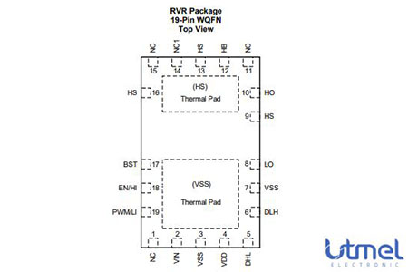
LMG1210 Pinout
LMG1210 CAD Model
Symbol
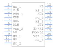
LMG1210 Symbol
Footprint
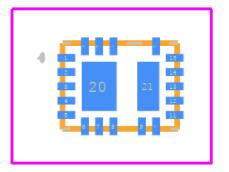
LMG1210 Footprint
3D Model
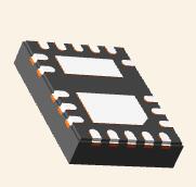
LMG1210 3D Model
LMG1210 Description
The LMG1210 is a 200-V, half-bridge MOSFET and Gallium Nitride Field Effect Transistor (GaN FET) driver designed for ultra-high frequency, high-efficiency applications that feature adjustable deadtime capability, very small propagation delay, and 3.4-ns high-side low-side matching to optimize system efficiency. This part also features an internal LDO that ensures a gate-drive voltage of 5-V regardless of the supply voltage.
LMG1210 Feature
• Up to 50-MHz operation
• 10-ns typical propagation delay
• 3.4-ns high-side to low-side matching
• Minimum pulse width of 4 ns
• Two control input options
– Single PWM input with adjustable dead time
– Independent input mode
• 1.5-A peak source and 3-A peak sink currents
• External bootstrap diode for flexibility
• Internal LDO for adaptability to voltage rails
• High 300-V/ns CMTI
• HO to LO capacitance less than 1 pF
• UVLO and overtemperature protection
• Low-inductance WQFN package
LMG1210 Functional Block Diagram
The LMG1210 provides numerous features optimized for driving external GaN FETs.
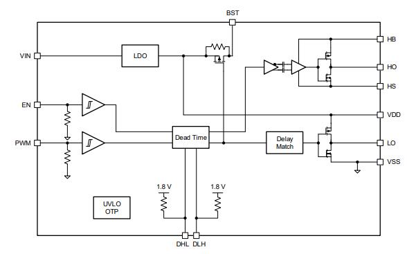
LMG1210 Functional Block Diagram
LMG1210 Application
• High-speed DC-DC converters
• RF envelope tracking
• Class-D audio amplifiers
• Class-E wireless charging
• High-precision motor control
LMG1210 Typical Application Circuit
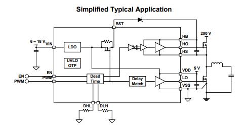
The LMG1210 is designed to optimally drive GaN FETs in half-bridge configurations, such as synchronous buck and boost converters, as well as more complex topologies. By integrating the level shifting and bootstrap operation the complexities of driving the high-side device are solved for the designer.
The list below shows some sample values for a typical 48 V to 12 V application synchronous buck.
• Input Voltage: 48 V
• Output Voltage: 12 V
• Output Current: 10 A
• Bias Voltage: 6 V
• Duty Cycle: 25 %
• Switching Frequency: 1 MHz
• Inductor: 4.7 µH
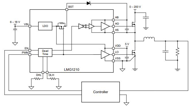
Simplified LMG1210 Configured as Synchronous Buck Converter
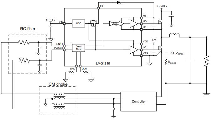
LMG1210 Configured With Current Sense Resistor Using a CMC as Filter
LMG1210 Package
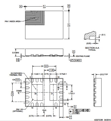
LMG1210 Dimension
Specifications
- TypeParameter
- Factory Lead Time6 Weeks
- Mounting Type
The "Mounting Type" in electronic components refers to the method used to attach or connect a component to a circuit board or other substrate, such as through-hole, surface-mount, or panel mount.
Surface Mount, Wettable Flank - Package / Case
refers to the protective housing that encases an electronic component, providing mechanical support, electrical connections, and thermal management.
19-WFQFN Exposed Pad - Surface Mount
having leads that are designed to be soldered on the side of a circuit board that the body of the component is mounted on.
YES - Driver ConfigurationHalf-Bridge
- Operating Temperature
The operating temperature is the range of ambient temperature within which a power supply, or any other electrical equipment, operate in. This ranges from a minimum operating temperature, to a peak or maximum operating temperature, outside which, the power supply may fail.
-40°C~125°C TJ - Packaging
Semiconductor package is a carrier / shell used to contain and cover one or more semiconductor components or integrated circuits. The material of the shell can be metal, plastic, glass or ceramic.
Tape & Reel (TR) - JESD-609 Code
The "JESD-609 Code" in electronic components refers to a standardized marking code that indicates the lead-free solder composition and finish of electronic components for compliance with environmental regulations.
e3 - Pbfree Code
The "Pbfree Code" parameter in electronic components refers to the code or marking used to indicate that the component is lead-free. Lead (Pb) is a toxic substance that has been widely used in electronic components for many years, but due to environmental concerns, there has been a shift towards lead-free alternatives. The Pbfree Code helps manufacturers and users easily identify components that do not contain lead, ensuring compliance with regulations and promoting environmentally friendly practices. It is important to pay attention to the Pbfree Code when selecting electronic components to ensure they meet the necessary requirements for lead-free applications.
yes - Part Status
Parts can have many statuses as they progress through the configuration, analysis, review, and approval stages.
Active - Moisture Sensitivity Level (MSL)
Moisture Sensitivity Level (MSL) is a standardized rating that indicates the susceptibility of electronic components, particularly semiconductors, to moisture-induced damage during storage and the soldering process, defining the allowable exposure time to ambient conditions before they require special handling or baking to prevent failures
2 (1 Year) - Number of Terminations19
- Terminal Finish
Terminal Finish refers to the surface treatment applied to the terminals or leads of electronic components to enhance their performance and longevity. It can improve solderability, corrosion resistance, and overall reliability of the connection in electronic assemblies. Common finishes include nickel, gold, and tin, each possessing distinct properties suitable for various applications. The choice of terminal finish can significantly impact the durability and effectiveness of electronic devices.
Matte Tin (Sn) - Voltage - Supply
Voltage - Supply refers to the range of voltage levels that an electronic component or circuit is designed to operate with. It indicates the minimum and maximum supply voltage that can be applied for the device to function properly. Providing supply voltages outside this range can lead to malfunction, damage, or reduced performance. This parameter is critical for ensuring compatibility between different components in a circuit.
6V~18V - Terminal Position
In electronic components, the term "Terminal Position" refers to the physical location of the connection points on the component where external electrical connections can be made. These connection points, known as terminals, are typically used to attach wires, leads, or other components to the main body of the electronic component. The terminal position is important for ensuring proper connectivity and functionality of the component within a circuit. It is often specified in technical datasheets or component specifications to help designers and engineers understand how to properly integrate the component into their circuit designs.
QUAD - Terminal Form
Occurring at or forming the end of a series, succession, or the like; closing; concluding.
NO LEAD - Number of Functions1
- Supply Voltage
Supply voltage refers to the electrical potential difference provided to an electronic component or circuit. It is crucial for the proper operation of devices, as it powers their functions and determines performance characteristics. The supply voltage must be within specified limits to ensure reliability and prevent damage to components. Different electronic devices have specific supply voltage requirements, which can vary widely depending on their design and intended application.
5V - Base Part Number
The "Base Part Number" (BPN) in electronic components serves a similar purpose to the "Base Product Number." It refers to the primary identifier for a component that captures the essential characteristics shared by a group of similar components. The BPN provides a fundamental way to reference a family or series of components without specifying all the variations and specific details.
LMG1210 - JESD-30 Code
JESD-30 Code refers to a standardized descriptive designation system established by JEDEC for semiconductor-device packages. This system provides a systematic method for generating designators that convey essential information about the package's physical characteristics, such as size and shape, which aids in component identification and selection. By using JESD-30 codes, manufacturers and engineers can ensure consistency and clarity in the specification of semiconductor packages across various applications and industries.
R-PQCC-N19 - Input Type
Input type in electronic components refers to the classification of the signal or data that a component can accept for processing or conversion. It indicates whether the input is analog, digital, or a specific format such as TTL or CMOS. Understanding input type is crucial for ensuring compatibility between different electronic devices and circuits, as it determines how signals are interpreted and interacted with.
TTL - Output Current-Max
Output Current-Max is a parameter in electronic components that specifies the maximum amount of current that can be safely drawn from the output of the component without causing damage. It is an important specification to consider when designing circuits to ensure that the component can handle the required current without overheating or failing. Exceeding the maximum output current can lead to performance issues, component damage, or even complete failure of the circuit. It is crucial to adhere to the specified maximum output current to ensure the reliable operation of the electronic component and the overall circuit.
3A - Rise / Fall Time (Typ)
The parameter "Rise / Fall Time (Typ)" in electronic components refers to the time it takes for a signal to transition from a specified low level to a specified high level (rise time) or from a high level to a low level (fall time). It is typically measured in nanoseconds or picoseconds and is an important characteristic in determining the speed and performance of a component, such as a transistor or integrated circuit. A shorter rise/fall time indicates faster signal switching and can impact the overall speed and efficiency of a circuit. Designers often consider this parameter when selecting components for high-speed applications to ensure proper signal integrity and timing.
500ps 500ps - Channel Type
In electronic components, the parameter "Channel Type" refers to the type of channel through which electrical signals or current flow within the component. This parameter is commonly associated with field-effect transistors (FETs) and other semiconductor devices. The channel type can be categorized as either N-channel or P-channel, depending on the polarity of the majority charge carriers (electrons or holes) that carry the current within the channel. N-channel devices have an electron-conducting channel, while P-channel devices have a hole-conducting channel. Understanding the channel type is crucial for proper circuit design and component selection to ensure compatibility and optimal performance.
Independent - Number of Drivers2
- Turn On Time
The time that it takes a gate circuit to allow a current to reach its full value.
0.018 µs - Output Peak Current Limit-Nom
Output Peak Current Limit-Nom is a parameter in electronic components that specifies the maximum current that can be delivered by the output under normal operating conditions. This limit is typically set to protect the component from damage due to excessive current flow. It ensures that the component operates within its safe operating limits and prevents overheating or other potential issues. Designers and engineers use this parameter to ensure proper functioning and reliability of the electronic system in which the component is used.
0.11A - Gate Type
In electronic components, the term "Gate Type" typically refers to the type of logic gate used in digital circuits. A logic gate is a fundamental building block of digital circuits that performs a specific logical operation based on the input signals it receives. Common types of logic gates include AND, OR, NOT, NAND, NOR, XOR, and XNOR gates.The Gate Type parameter specifies the specific logic function that the gate performs, such as AND, OR, or NOT. Different gate types have different truth tables that define their behavior based on the input signals. By selecting the appropriate gate type for a given application, designers can implement various logical functions and operations in digital circuits.Understanding the gate type is essential for designing and analyzing digital circuits, as it determines how the circuit processes and manipulates binary data. Choosing the right gate type is crucial for ensuring the correct functionality and performance of the digital system being designed.
N-Channel MOSFET - Current - Peak Output (Source, Sink)
The parameter "Current - Peak Output (Source, Sink)" in electronic components refers to the maximum amount of current that the component can either supply (source) or sink (absorb) under peak conditions. This parameter is important for understanding the capability of the component to handle sudden surges or spikes in current without being damaged. The peak output current is typically specified in datasheets and is crucial for designing circuits that require high current handling capabilities. It is essential to consider this parameter to ensure the component operates within its safe operating limits and to prevent potential damage or malfunction.
1.5A 3A - Turn Off Time
Turn Off Time is a parameter in electronic components, particularly in devices like transistors and diodes. It refers to the time taken for the component to switch from an ON state to an OFF state when a control signal is applied. This parameter is crucial in determining the speed and efficiency of the component's operation. A shorter turn off time indicates faster switching speeds, which is important in applications where rapid switching is required, such as in power electronics and digital circuits. Manufacturers provide this specification in datasheets to help engineers and designers select the right components for their specific requirements.
0.018 µs - Built-in Protections
Built-in protections in electronic components refer to the safety features and mechanisms that are integrated into the component to prevent damage or malfunction in various situations. These protections are designed to safeguard the component from overvoltage, overcurrent, overheating, short circuits, and other potential hazards that could occur during operation. By having built-in protections, electronic components can operate more reliably and safely, extending their lifespan and reducing the risk of failure. These protections are essential for ensuring the overall performance and longevity of electronic devices and systems.
THERMAL; UNDER VOLTAGE - High Side Voltage - Max (Bootstrap)
The parameter "High Side Voltage - Max (Bootstrap)" in electronic components refers to the maximum voltage that can be applied to the high side of a bootstrap circuit. Bootstrap circuits are commonly used in power electronics to drive high-side MOSFETs or IGBTs efficiently. This parameter is crucial for ensuring the proper operation and reliability of the bootstrap circuit, as exceeding the maximum voltage can lead to component failure or malfunction. Designers must carefully consider this specification when selecting components and designing circuits to prevent damage and ensure optimal performance.
200V - Output Current Flow Direction
Output Current Flow Direction refers to the orientation of current flowing out of a component or circuit. It indicates whether the current is being sourced from the component or sent to another component in the circuit. This parameter is crucial for understanding how electronic components interact within a circuit and ensures correct connectivity and functionality in circuit design. The direction can affect the operation and performance of the overall system.
SOURCE SINK - Length4mm
- Height Seated (Max)
Height Seated (Max) is a parameter in electronic components that refers to the maximum allowable height of the component when it is properly seated or installed on a circuit board or within an enclosure. This specification is crucial for ensuring proper fit and alignment within the overall system design. Exceeding the maximum seated height can lead to mechanical interference, electrical shorts, or other issues that may impact the performance and reliability of the electronic device. Manufacturers provide this information to help designers and engineers select components that will fit within the designated space and function correctly in the intended application.
0.8mm - Width3mm
- RoHS Status
RoHS means “Restriction of Certain Hazardous Substances” in the “Hazardous Substances Directive” in electrical and electronic equipment.
ROHS3 Compliant
Datasheet PDF
- Other Related Documents :
- PCN Design/Specification :
What allows the designer to choose the optimal bootstrap diode to charge the high-side bootstrap capacitor?
LMG1210.
What two control input modes does the LMG1210 have?
Independent Input Mode (IIM) and PWM mode.
What controls the outputs of the LMG1210?
Dedicated input.
What is the dead time for each edge of the LMG1210?
0 to 20 ns.
What type of package is the LMG1210 offered in?
Low-inductance WQFN.
What are some of the features of the LMG1210 designed to drive GaN FETs in half-bridge configurations?
Synchronous buck and boost converters.
What are the components of the LMG1210 that solve the complexities of driving the high-side device?
Level shifting and bootstrap operation.
 TL074ID OP-AMP: Pinout, Specification, and Datasheet
11 June 20214483
![Arduino Giga R1 WiFi: Specifications, Features and Applications[FAQs]](https://res.utmel.com/Images/Article/7318ed8c-3aef-4191-9c57-9aaf6fb034ce.png) Arduino Giga R1 WiFi: Specifications, Features and Applications[FAQs]
Arduino Giga R1 WiFi: Specifications, Features and Applications[FAQs]06 October 202310897
 MMBTA42 NPN High-Voltage Transistor: NPN, SOT-23, Datasheet
07 February 20222281
 Realtek RTD1296: 4K Smart TV Box Solution
29 February 2024969
 LM74700QDBVRQ1 Diode Controller: 12V, Pinout, Datasheet
07 March 20224744
 ZiLOG ZLP12840 OTP MCU: Product Overview
29 February 2024264
 A Comprehensive Guide to DIABLO16 Microcontroller by 4D Systems Pty Ltd
07 March 2024590
 IRF1404 Power MOSFET: Datasheet, IRF1404, IRF1404 vs. IRF3205
24 November 202119530
 CR1220 Battery User Reviews on Leading Brands
21 August 20252771
 Circuit Breaker: Working Principle, Types and Structure
21 November 202512097
 MLCC vs Polymer Tantalum Capacitors: Overcoming 2026 Shortages in AI Server PDNs
07 August 2026511
 New Technology Helps Detect and Prevent Automated Browsing
13 November 20232628
 What is a variable capacitor?
16 April 202566365
 Global Semiconductor Sales Experience a 2.3% Surge in July 2023
09 September 20233893
 Using Microcontrollers in the Internet of Things (IoT) Applications
27 June 20236658
 Understanding Machine Vision and Visual Sensor
27 September 20212280
Texas Instruments
In Stock: 65
United States
China
Canada
Japan
Russia
Germany
United Kingdom
Singapore
Italy
Hong Kong(China)
Taiwan(China)
France
Korea
Mexico
Netherlands
Malaysia
Austria
Spain
Switzerland
Poland
Thailand
Vietnam
India
United Arab Emirates
Afghanistan
Åland Islands
Albania
Algeria
American Samoa
Andorra
Angola
Anguilla
Antigua & Barbuda
Argentina
Armenia
Aruba
Australia
Azerbaijan
Bahamas
Bahrain
Bangladesh
Barbados
Belarus
Belgium
Belize
Benin
Bermuda
Bhutan
Bolivia
Bonaire, Sint Eustatius and Saba
Bosnia & Herzegovina
Botswana
Brazil
British Indian Ocean Territory
British Virgin Islands
Brunei
Bulgaria
Burkina Faso
Burundi
Cabo Verde
Cambodia
Cameroon
Cayman Islands
Central African Republic
Chad
Chile
Christmas Island
Cocos (Keeling) Islands
Colombia
Comoros
Congo
Congo (DRC)
Cook Islands
Costa Rica
Côte d’Ivoire
Croatia
Cuba
Curaçao
Cyprus
Czechia
Denmark
Djibouti
Dominica
Dominican Republic
Ecuador
Egypt
El Salvador
Equatorial Guinea
Eritrea
Estonia
Eswatini
Ethiopia
Falkland Islands
Faroe Islands
Fiji
Finland
French Guiana
French Polynesia
Gabon
Gambia
Georgia
Ghana
Gibraltar
Greece
Greenland
Grenada
Guadeloupe
Guam
Guatemala
Guernsey
Guinea
Guinea-Bissau
Guyana
Haiti
Honduras
Hungary
Iceland
Indonesia
Iran
Iraq
Ireland
Isle of Man
Israel
Jamaica
Jersey
Jordan
Kazakhstan
Kenya
Kiribati
Kosovo
Kuwait
Kyrgyzstan
Laos
Latvia
Lebanon
Lesotho
Liberia
Libya
Liechtenstein
Lithuania
Luxembourg
Macao(China)
Madagascar
Malawi
Maldives
Mali
Malta
Marshall Islands
Martinique
Mauritania
Mauritius
Mayotte
Micronesia
Moldova
Monaco
Mongolia
Montenegro
Montserrat
Morocco
Mozambique
Myanmar
Namibia
Nauru
Nepal
New Caledonia
New Zealand
Nicaragua
Niger
Nigeria
Niue
Norfolk Island
North Korea
North Macedonia
Northern Mariana Islands
Norway
Oman
Pakistan
Palau
Palestinian Authority
Panama
Papua New Guinea
Paraguay
Peru
Philippines
Pitcairn Islands
Portugal
Puerto Rico
Qatar
Réunion
Romania
Rwanda
Samoa
San Marino
São Tomé & Príncipe
Saudi Arabia
Senegal
Serbia
Seychelles
Sierra Leone
Sint Maarten
Slovakia
Slovenia
Solomon Islands
Somalia
South Africa
South Sudan
Sri Lanka
St Helena, Ascension, Tristan da Cunha
St. Barthélemy
St. Kitts & Nevis
St. Lucia
St. Martin
St. Pierre & Miquelon
St. Vincent & Grenadines
Sudan
Suriname
Svalbard & Jan Mayen
Sweden
Syria
Tajikistan
Tanzania
Timor-Leste
Togo
Tokelau
Tonga
Trinidad & Tobago
Tunisia
Turkey
Turkmenistan
Turks & Caicos Islands
Tuvalu
U.S. Outlying Islands
U.S. Virgin Islands
Uganda
Ukraine
Uruguay
Uzbekistan
Vanuatu
Vatican City
Venezuela
Wallis & Futuna
Yemen
Zambia
Zimbabwe
![LM5060MM/NOPB]() LM5060MM/NOPB
LM5060MM/NOPBTexas Instruments
![LM5109BMAX/NOPB]() LM5109BMAX/NOPB
LM5109BMAX/NOPBTexas Instruments
![LM5105SD/NOPB]() LM5105SD/NOPB
LM5105SD/NOPBTexas Instruments
![LM5106MM/NOPB]() LM5106MM/NOPB
LM5106MM/NOPBTexas Instruments
![LM5060Q1MM/NOPB]() LM5060Q1MM/NOPB
LM5060Q1MM/NOPBTexas Instruments
![LM5101ASD/NOPB]() LM5101ASD/NOPB
LM5101ASD/NOPBTexas Instruments
![LM5060Q1MMX/NOPB]() LM5060Q1MMX/NOPB
LM5060Q1MMX/NOPBTexas Instruments
![UCC27517DBVR]() UCC27517DBVR
UCC27517DBVRTexas Instruments
![UCC27201DDAR]() UCC27201DDAR
UCC27201DDARTexas Instruments
![LM5104MX/NOPB]() LM5104MX/NOPB
LM5104MX/NOPBTexas Instruments


