
 Product
 Brand
Brand Articles
 Tools
Tools
TL494 PWM Controller: Technical Guide, Datasheet Analysis, and Circuit Design


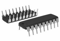
7V~40V 16-Pin TL494 DC to DC converter IC 2 Outputs 1kHz~300kHz Transistor Driver
The TL494 is the industry-standard fixed-frequency PWM controller for switched-mode power supplies. This guide covers specs, pinout, circuit design, and troubleshooting.
Product Introduction
Engineer's Takeaway
Positioning: The TL494 is the foundational "Swiss Army Knife" of PWM control. While older than modern digital controllers, it remains the dominant choice for cost-sensitive, specific-topology power supplies (buck/boost/half-bridge) due to its architectural flexibility.
Key Spec Highlight: Integrated uncommitted output transistors capable of sourcing or sinking 200mA, allowing direct drive of small loads or bipolar transistors.
Supply Chain Status: High Availability. This is a commodity component with massive stock levels and multiple generic sources (TI, ONsemi, STM), making it immune to single-source shortages.
1. Technical Architecture and Core Advantages
The TL494 is a fixed-frequency pulse-width-modulation (PWM) control circuit on a single chip. Unlike modern current-mode controllers, the TL494 utilizes voltage-mode control, modulating the pulse width by comparing a sawtooth waveform (generated by an internal oscillator) against feedback voltage levels.
1.1 Processing & Control (The "Brain")
The core control logic relies on an internal oscillator and two error amplifiers. - Oscillator strategy: The frequency is programmable from 1kHz to 300kHz using an external timing resistor (Rt) and capacitor (Ct). The ramp is generated at the capacitor (Pin 5).
Control Loop: It features two error amplifiers. In most PSU designs, one amplifier regulates the output voltage, while the second limits output current (overcurrent protection). Their outputs are diode-ORed, meaning the amplifier demanding the narrowest pulse width dominates the loop.
1.2 Peripherals & Interfaces (The "Limbs")
The chip integrates essential power management blocks to reduce external component count:
5V Reference Regulator: An internal bandgap generating 5V ±5% (stable over 0°C to 70°C) to bias external sensors or dividers.
Output Control Logic: A dedicated pin (Pin 13) allows the designer to select between:
Single-Ended Operation: Both outputs switch in parallel.
Push-Pull Operation: Outputs switch alternately (essential for half-bridge or push-pull topologies).
Dead-Time Control (DTC): Pin 4 provides a direct input to force a minimum "off" time, preventing shoot-through currents in bridge topologies.

Figure 1: TL494 functional block diagram internal architecture
2. Naming / Variant Map and Selection Guide
2.1 Part Number Decoding
The TL494 follows Texas Instruments' standard naming convention.
- Prefix:
- TL: Standard Linear
- Operating Temperature:
- C: Commercial (0°C to 70°C)
- I: Industrial (-40°C to 85°C)
- Package Suffix:
- N: PDIP-16 (Plastic Dual In-Line Package) - Best for breadboarding.
- D: SOIC-16 (Small Outline Integrated Circuit) - Surface mount.
- PW: TSSOP-16 (Thin Shrink Small Outline) - Low profile.
2.2 Core Variant Comparison
| Variant | Key Differences | Flash/RAM | Package | Target Use |
|---|---|---|---|---|
| TL494CN | Commercial Temp (0°C to 70°C) | N/A (Analog) | PDIP-16 | Prototyping, Repair, Legacy |
| TL494CD | Commercial Temp (0°C to 70°C) | N/A (Analog) | SOIC-16 | Consumer Electronics |
| TL494IN | Industrial Temp (-40°C to 85°C) | N/A (Analog) | PDIP-16 | Industrial Power Supplies, Outdoor |
| TL494CPW | Commercial Temp (0°C to 70°C) | N/A (Analog) | TSSOP-16 | Space-constrained Layouts |
3. Key Specifications Explained
Engineer's Note: Values below are typical based on the TI datasheet. Always consult the specific datasheet for max/min limits, especially when using clones (e.g., KA7500).
3.1 Power & Operating Conditions
The TL494 is designed for mid-voltage DC environments. - Supply Voltage (VCC): 7V to 40V. - Design Implication: It is ideal for 12V and 24V automotive or industrial rails. For 48V systems, a pre-regulator or zener drop is strictly required to prevent dielectric breakdown. - Maximum Output Voltage: 40V at the collector/emitter.
3.2 Performance & Efficiency
Since this is an analog controller, "performance" relates to drive capability and timing precision rather than logic cells. - Output Drive: Can sink or source 200mA per channel. - Reference Accuracy: 5V Reference is tight (±5%), which is critical for maintaining precise output voltage regulation without external precision references. - Duty Cycle: Variable from 0% to approx 45% (Push-Pull) or 96% (Single-Ended).

Figure 2: TL494 Typical performance characteristics (Oscillator Frequency vs Timing Resistance)
4. Design Notes and Common Integration Issues
4.1 PCB Layout Guidelines
Power Rails: Place a 0.1µF to 1µF ceramic capacitor as close as possible to Pin 12 (VCC) and Pin 7 (GND) to shunt high-frequency switching noise.
Grounding: Separate "Signal Ground" (Oscillator, Error Amp feedback) from "Power Ground" (Output emitters). Join them at a single star point at the chip ground pin to prevent ground bounce from affecting the control logic.
Oscillator: Keep the traces for Rt and Ct (Pins 5 and 6) distinct and short. Stray capacitance here will cause frequency drift.
4.2 Debugging Common Faults (Pain Points)
The following are frequent issues encountered during system integration, derived from engineering support logs.
Problem 1: Insufficient Drive for High-Power MOSFETs- Symptom: MOSFETs overheat, switching losses are high, or edges are slow. - Root Cause: The TL494 internal transistors are limited to 200mA. Large power MOSFETs have high gate capacitance requiring peaks of 1A+ for fast switching. - Fix: Implement an external totem-pole driver (NPN+PNP pair) or a dedicated gate driver IC between the TL494 and the MOSFET gate.
Problem 2: Output Glitching / Instability- Symptom: Unexpected pulses during startup or erratic behavior. - Root Cause: Noise coupling into the Dead Time Control (DTC) pin or Vref instability. - Fix: Ensure proper decoupling of VCC. Verify pin 4 (DTC) is not floating; it must be biased generally to ground or a soft-start capacitor circuit.
Problem 3: Regulation Drift- Symptom: Output voltage sags under load or behaves non-linearly. - Root Cause: The Error Amplifier inputs have high impedance, but loading them with low-impedance dividers affects internal biasing. - Fix: Use lower resistance values for feedback networks or buffer the input if using high-value resistors for power savings.
5. Typical Applications
📺 Video Recommendation: TL494 Guide
5.1 System Integration Analysis: Half-Bridge SMPS
One of the most common uses for the TL494 is in PC Power Supplies (ATX) using a half-bridge topology. - Why TL494? The efficient Push-Pull mode (via Pin 13) automatically handles the alternating switching required for the two primary transistors. - Dead Time: The variable dead time (Pin 4) is critical here to ensure one transistor turns off completely before the other turns on, preventing a catastrophic short circuit across the supply rail. - Regulation: One error amplifier monitors the +5V or +12V rail, while the second amplifier monitors a current sense resistor to provide overload protection.

Figure 3: TL494 Typical application circuit: 5V/10A Switching Power Supply
6. Competitors and Alternatives
The PWM controller market is vast, but the TL494 holds a specific legacy niche.
- Vs. SG3525: The SG3525 is a slightly more modern alternative. - Difference: SG3525 features Totem-pole outputs natively, meaning it can drive MOSFETs harder directly without external BJTs. TL494 requires external buffering for high-capacitance gates.
- Vs. KA7500B: - Relationship: The KA7500B (Fairchild/ONsemi) is effectively a direct clone of the TL494. They are pin-compatible and functionally identical in most circuits.
- Vs. UC3843: - Difference: The UC3843 is a Current-Mode controller. It offers faster transient response and simpler loop compensation but is architecturally different and not a drop-in replacement.
7. FAQ
Q: What is the absolute maximum voltage for the TL494? The absolute maximum supply voltage (VCC) and collector voltage is 41V, but recommended design limits should not exceed 40V.
Q: Can the TL494 drive MOSFETs directly? Yes, but with caveats. Limited to 200mA, it can drive small MOSFETs. For high-power switching, external gate drivers or totem-pole buffers are required to ensure fast switching speeds.
Q: How do I enable Push-Pull operation on the TL494? Connect the Output Control pin (Pin 13) to the Vref pin (Pin 14). This directs the pulse steering flip-flop to alternate the outputs.
Q: What is the primary difference between TL494 and TL594? The TL594 is an improved version of the TL494 with higher precision error amplifiers and an improved output control circuit, but the TL494 remains far more ubiquitous.
8. Resources and Downloads
Datasheet: TL494-556737 PDF
Dev Tools: Look for "TL494 Module" or "Inverter Driver Board" on distributor sites for quick prototyping.
Specifications
- TypeParameter
- Factory Lead Time6 Weeks
- Mounting Type
The "Mounting Type" in electronic components refers to the method used to attach or connect a component to a circuit board or other substrate, such as through-hole, surface-mount, or panel mount.
Through Hole - Package / Case
refers to the protective housing that encases an electronic component, providing mechanical support, electrical connections, and thermal management.
16-DIP (0.300, 7.62mm) - Number of Pins16
- Operating Temperature
The operating temperature is the range of ambient temperature within which a power supply, or any other electrical equipment, operate in. This ranges from a minimum operating temperature, to a peak or maximum operating temperature, outside which, the power supply may fail.
-40°C~85°C TA - Packaging
Semiconductor package is a carrier / shell used to contain and cover one or more semiconductor components or integrated circuits. The material of the shell can be metal, plastic, glass or ceramic.
Tube - Part Status
Parts can have many statuses as they progress through the configuration, analysis, review, and approval stages.
Active - Moisture Sensitivity Level (MSL)
Moisture Sensitivity Level (MSL) is a standardized rating that indicates the susceptibility of electronic components, particularly semiconductors, to moisture-induced damage during storage and the soldering process, defining the allowable exposure time to ambient conditions before they require special handling or baking to prevent failures
1 (Unlimited) - Frequency
In electronic components, the parameter "Frequency" refers to the rate at which a signal oscillates or cycles within a given period of time. It is typically measured in Hertz (Hz) and represents how many times a signal completes a full cycle in one second. Frequency is a crucial aspect in electronic components as it determines the behavior and performance of various devices such as oscillators, filters, and communication systems. Understanding the frequency characteristics of components is essential for designing and analyzing electronic circuits to ensure proper functionality and compatibility with other components in a system.
300kHz - Base Part Number
The "Base Part Number" (BPN) in electronic components serves a similar purpose to the "Base Product Number." It refers to the primary identifier for a component that captures the essential characteristics shared by a group of similar components. The BPN provides a fundamental way to reference a family or series of components without specifying all the variations and specific details.
TL494 - Function
The parameter "Function" in electronic components refers to the specific role or purpose that the component serves within an electronic circuit. It defines how the component interacts with other elements, influences the flow of electrical signals, and contributes to the overall behavior of the system. Functions can include amplification, signal processing, switching, filtering, and energy storage, among others. Understanding the function of each component is essential for designing effective and efficient electronic systems.
Step-Up, Step-Down, Step-Up/Step-Down - Number of Outputs2
- Output Voltage
Output voltage is a crucial parameter in electronic components that refers to the voltage level produced by the component as a result of its operation. It represents the electrical potential difference between the output terminal of the component and a reference point, typically ground. The output voltage is a key factor in determining the performance and functionality of the component, as it dictates the level of voltage that will be delivered to the connected circuit or load. It is often specified in datasheets and technical specifications to ensure compatibility and proper functioning within a given system.
40V - Output Type
The "Output Type" parameter in electronic components refers to the type of signal or data that is produced by the component as an output. This parameter specifies the nature of the output signal, such as analog or digital, and can also include details about the voltage levels, current levels, frequency, and other characteristics of the output signal. Understanding the output type of a component is crucial for ensuring compatibility with other components in a circuit or system, as well as for determining how the output signal can be utilized or processed further. In summary, the output type parameter provides essential information about the nature of the signal that is generated by the electronic component as its output.
Transistor Driver - Output Configuration
Output Configuration in electronic components refers to the arrangement or setup of the output pins or terminals of a device. It defines how the output signals are structured and how they interact with external circuits or devices. The output configuration can determine the functionality and compatibility of the component in a circuit design. Common types of output configurations include single-ended, differential, open-drain, and push-pull configurations, each serving different purposes and applications in electronic systems. Understanding the output configuration of a component is crucial for proper integration and operation within a circuit.
Positive - Output Current
The rated output current is the maximum load current that a power supply can provide at a specified ambient temperature. A power supply can never provide more current that it's rated output current unless there is a fault, such as short circuit at the load.
200mA - Voltage - Supply (Vcc/Vdd)
Voltage - Supply (Vcc/Vdd) is a key parameter in electronic components that specifies the voltage level required for the proper operation of the device. It represents the power supply voltage that needs to be provided to the component for it to function correctly. This parameter is crucial as supplying the component with the correct voltage ensures that it operates within its specified limits and performance characteristics. It is typically expressed in volts (V) and is an essential consideration when designing and using electronic circuits to prevent damage and ensure reliable operation.
7V~40V - Control Features
Control features in electronic components refer to specific functionalities or characteristics that allow users to manage and regulate the operation of the component. These features are designed to provide users with control over various aspects of the component's performance, such as adjusting settings, monitoring parameters, or enabling specific modes of operation. Control features can include options for input/output configurations, power management, communication protocols, and other settings that help users customize and optimize the component's behavior according to their requirements. Overall, control features play a crucial role in enhancing the flexibility, usability, and performance of electronic components in various applications.
Dead Time Control, Frequency Control - Topology
In the context of electronic components, "topology" refers to the arrangement or configuration of the components within a circuit or system. It defines how the components are connected to each other and how signals flow between them. The choice of topology can significantly impact the performance, efficiency, and functionality of the electronic system. Common topologies include series, parallel, star, mesh, and hybrid configurations, each with its own advantages and limitations. Designers carefully select the appropriate topology based on the specific requirements of the circuit to achieve the desired performance and functionality.
Buck, Boost, Flyback, Forward Converter, Full-Bridge, Half-Bridge, Push-Pull - Frequency - Switching
"Frequency - Switching" in electronic components refers to the rate at which a device, such as a transistor or switching regulator, turns on and off during operation. This parameter is crucial in determining the efficiency and performance of power converters, oscillators, and other circuits that rely on rapid switching. Higher switching frequencies typically allow for smaller component sizes but may require more advanced design considerations to manage heat and electromagnetic interference.
1kHz~300kHz - Synchronous Rectifier
Synchronous rectification is a technique for improving the efficiency of rectification by replacing diodes with actively controlled switches, usually power MOSFETs or power bipolar junction transistors (BJT).
No - Nominal Input Voltage
The actual voltage at which a circuit operates can vary from the nominal voltage within a range that permits satisfactory operation of equipment. The word “nominal” means “named”.
15V - Duty Cycle (Max)
The "Duty Cycle (Max)" parameter in electronic components refers to the maximum percentage of time that a signal is active or on within a specific period. It is commonly used in components such as pulse-width modulation (PWM) controllers, oscillators, and timers. A duty cycle of 100% means the signal is always on, while a duty cycle of 0% means the signal is always off. Understanding the maximum duty cycle is important for ensuring proper operation and performance of the electronic component within its specified limits. It is typically expressed as a percentage and helps determine the amount of power or energy being delivered by the signal.
45% - Output Phases
Output Phases in electronic components refer to the number of distinct output signals or waveforms that the component can generate. This parameter is commonly associated with devices such as power inverters, motor drives, and signal generators. The output phases indicate how many separate signals can be produced simultaneously by the component, with each phase typically representing a different electrical waveform or signal. Understanding the output phases of an electronic component is important for designing and implementing systems that require multiple output signals or for ensuring compatibility with other components in a circuit.
1 - REACH SVHC
The parameter "REACH SVHC" in electronic components refers to the compliance with the Registration, Evaluation, Authorization, and Restriction of Chemicals (REACH) regulation regarding Substances of Very High Concern (SVHC). SVHCs are substances that may have serious effects on human health or the environment, and their use is regulated under REACH to ensure their safe handling and minimize their impact.Manufacturers of electronic components need to declare if their products contain any SVHCs above a certain threshold concentration and provide information on the safe use of these substances. This information allows customers to make informed decisions about the potential risks associated with using the components and take appropriate measures to mitigate any hazards.Ensuring compliance with REACH SVHC requirements is essential for electronics manufacturers to meet regulatory standards, protect human health and the environment, and maintain transparency in their supply chain. It also demonstrates a commitment to sustainability and responsible manufacturing practices in the electronics industry.
No SVHC - RoHS Status
RoHS means “Restriction of Certain Hazardous Substances” in the “Hazardous Substances Directive” in electrical and electronic equipment.
ROHS3 Compliant
Parts with Similar Specs
- ImagePart NumberManufacturerPackage / CaseNumber of PinsNumber of OutputsOutput CurrentFrequency - SwitchingNominal Input VoltageMoisture Sensitivity Level (MSL)Output TypeView Compare
![TL494ING4]()
TL494ING4
16-DIP (0.300, 7.62mm)
16
2
200 mA
1kHz ~ 300kHz
15 V
1 (Unlimited)
Transistor Driver
![TL594CN]()
16-DIP (0.300, 7.62mm)
16
1
250 mA
1kHz ~ 200kHz
-
1 (Unlimited)
Transistor Driver
![KA3525A]()
16-DIP (0.300, 7.62mm)
16
2
500 mA
60Hz ~ 430kHz
-
1 (Unlimited)
Transistor Driver
![KA7500B]()
16-DIP (0.300, 7.62mm)
16
2
500 mA
-
-
1 (Unlimited)
Transistor Driver
![KA7500C]()
16-DIP (0.300, 7.62mm)
16
1
250 mA
1kHz ~ 300kHz
-
1 (Unlimited)
Transistor Driver


Datasheet PDF
- Datasheets :
![LR41 Battery, LR41 Battery Equivalent, LR41 and SR41 Cell Battery [FAQ]](https://res.utmel.com/Images/Article/edaf2000-e788-42b0-b239-6f7d52115528.jpg) LR41 Battery, LR41 Battery Equivalent, LR41 and SR41 Cell Battery [FAQ]
LR41 Battery, LR41 Battery Equivalent, LR41 and SR41 Cell Battery [FAQ]20 December 202133059
 LM3914N Display Driver: Datasheet, Pinout and Comparison
02 August 20218124
 BHI160 Sensor: Pinout, Features, and Datasheet
14 August 20241792
 SN74LVC1G17QDCKRQ1 Schmitt-Trigger Buffer: Diagram, Pinout, and Datasheet
06 April 20223906
 AK8963 Electronic Compass: Pinout, Datasheet and Features
16 July 20212231
 TDA8356 Power Circuit: Equivalent, Pinout, Datasheet
18 March 202211077
 Audio Amplifier IC LM386:Where/How to use?
05 May 202211871
 M4T28-BR12SH1 Battery: M4T28-BR12SH1 Datasheet, Logic Diagram
07 March 20223326
 The World's Top 10 Innovative LED Drivers
12 February 20224894
 What is a Fiber Optic Connector?
27 October 20257906
 Basic Introduction to System on a Chip
02 December 20204594
 UMD Receives $2M NSF Grant for Advancement of Semiconductor Technology and Workforce Training
27 September 20233866
 A Selection of the Most Representative Charts——Artificial Intelligence Index Report
18 March 2022941
 Switching Diodes Basics: Working, Types and Circuit Analysis
24 October 202542519
 What is Tantalum Capacitor: Structure, Failure and Application Guide
14 April 202220675
 What is a DC-to-DC Converter?
23 April 20217442
Texas Instruments
In Stock: 29
United States
China
Canada
Japan
Russia
Germany
United Kingdom
Singapore
Italy
Hong Kong(China)
Taiwan(China)
France
Korea
Mexico
Netherlands
Malaysia
Austria
Spain
Switzerland
Poland
Thailand
Vietnam
India
United Arab Emirates
Afghanistan
Åland Islands
Albania
Algeria
American Samoa
Andorra
Angola
Anguilla
Antigua & Barbuda
Argentina
Armenia
Aruba
Australia
Azerbaijan
Bahamas
Bahrain
Bangladesh
Barbados
Belarus
Belgium
Belize
Benin
Bermuda
Bhutan
Bolivia
Bonaire, Sint Eustatius and Saba
Bosnia & Herzegovina
Botswana
Brazil
British Indian Ocean Territory
British Virgin Islands
Brunei
Bulgaria
Burkina Faso
Burundi
Cabo Verde
Cambodia
Cameroon
Cayman Islands
Central African Republic
Chad
Chile
Christmas Island
Cocos (Keeling) Islands
Colombia
Comoros
Congo
Congo (DRC)
Cook Islands
Costa Rica
Côte d’Ivoire
Croatia
Cuba
Curaçao
Cyprus
Czechia
Denmark
Djibouti
Dominica
Dominican Republic
Ecuador
Egypt
El Salvador
Equatorial Guinea
Eritrea
Estonia
Eswatini
Ethiopia
Falkland Islands
Faroe Islands
Fiji
Finland
French Guiana
French Polynesia
Gabon
Gambia
Georgia
Ghana
Gibraltar
Greece
Greenland
Grenada
Guadeloupe
Guam
Guatemala
Guernsey
Guinea
Guinea-Bissau
Guyana
Haiti
Honduras
Hungary
Iceland
Indonesia
Iran
Iraq
Ireland
Isle of Man
Israel
Jamaica
Jersey
Jordan
Kazakhstan
Kenya
Kiribati
Kosovo
Kuwait
Kyrgyzstan
Laos
Latvia
Lebanon
Lesotho
Liberia
Libya
Liechtenstein
Lithuania
Luxembourg
Macao(China)
Madagascar
Malawi
Maldives
Mali
Malta
Marshall Islands
Martinique
Mauritania
Mauritius
Mayotte
Micronesia
Moldova
Monaco
Mongolia
Montenegro
Montserrat
Morocco
Mozambique
Myanmar
Namibia
Nauru
Nepal
New Caledonia
New Zealand
Nicaragua
Niger
Nigeria
Niue
Norfolk Island
North Korea
North Macedonia
Northern Mariana Islands
Norway
Oman
Pakistan
Palau
Palestinian Authority
Panama
Papua New Guinea
Paraguay
Peru
Philippines
Pitcairn Islands
Portugal
Puerto Rico
Qatar
Réunion
Romania
Rwanda
Samoa
San Marino
São Tomé & Príncipe
Saudi Arabia
Senegal
Serbia
Seychelles
Sierra Leone
Sint Maarten
Slovakia
Slovenia
Solomon Islands
Somalia
South Africa
South Sudan
Sri Lanka
St Helena, Ascension, Tristan da Cunha
St. Barthélemy
St. Kitts & Nevis
St. Lucia
St. Martin
St. Pierre & Miquelon
St. Vincent & Grenadines
Sudan
Suriname
Svalbard & Jan Mayen
Sweden
Syria
Tajikistan
Tanzania
Timor-Leste
Togo
Tokelau
Tonga
Trinidad & Tobago
Tunisia
Turkey
Turkmenistan
Turks & Caicos Islands
Tuvalu
U.S. Outlying Islands
U.S. Virgin Islands
Uganda
Ukraine
Uruguay
Uzbekistan
Vanuatu
Vatican City
Venezuela
Wallis & Futuna
Yemen
Zambia
Zimbabwe
![LM3485MM/NOPB]() LM3485MM/NOPB
LM3485MM/NOPBTexas Instruments
![LM3478MM/NOPB]() LM3478MM/NOPB
LM3478MM/NOPBTexas Instruments
![LM5085MY/NOPB]() LM5085MY/NOPB
LM5085MY/NOPBTexas Instruments
![UC2825DW]() UC2825DW
UC2825DWTexas Instruments
![UCC28950PWR]() UCC28950PWR
UCC28950PWRTexas Instruments
![LM3488MM/NOPB]() LM3488MM/NOPB
LM3488MM/NOPBTexas Instruments
![UC3845AD8]() UC3845AD8
UC3845AD8Texas Instruments
![LM3150MHX/NOPB]() LM3150MHX/NOPB
LM3150MHX/NOPBTexas Instruments
![UCC28C43DR]() UCC28C43DR
UCC28C43DRTexas Instruments
![UCC25600DR]() UCC25600DR
UCC25600DRTexas Instruments


