
 Product
 Brand
Brand Articles
 Tools
Tools
KA7500B Controller: Features, Pinout, and Datasheet [Video&FAQ]

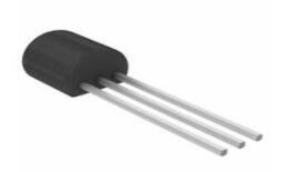
16 Terminals 7V~42V 16-Pin KA7500 DC to DC converter IC SWITCHING CONTROLLER 1 Outputs 1kHz~300kHz Transistor Driver


16 Terminals 7V~42V 16-Pin KA7500 DC to DC converter IC SWITCHING CONTROLLER 1 Outputs 1kHz~300kHz Transistor Driver
Hello guys. The KA7500B is used for the control circuit of the PWM switching regulator. This article mainly introduces features, pinout, datasheet and other detailed information about ON Semiconductor KA7500B.

How to test TL494 / KA7500 PWM Controller IC
KA7500B Description
The KA7500B is used for the control circuit of the PWM switching regulator. The KA7500B consists of a 5V reference voltage circuit, two error amplifiers, a flip flop, an output control circuit, a PWM comparator, a dead time comparator and an oscillator. This device can be operated in the switching frequency of 1kHz to 300kHz.
KA7500B Pinout

Pinout
| Pin Number | Pin Name | Description |
| 1 | 1IN+ | The non-inverting input terminal of error amplifier 1. In the closed-loop system, the given signal of the controlled quantity will be input to the error amplifier through this pin, while in the open-loop system, the pin needs to be grounded or left floating. |
| 2 | 1IN- | The inverting input terminal of the error amplifier 1. In the closed-loop system, the feedback signal of the controlled quantity will be input into the error amplifier through this pin. At this time, it is also necessary to connect the feedback network between this pin and pin 3. In the open-loop system, this pin is grounded or left floating. |
| 3 | FEEDBACK | Feedback/PWM comparator input terminal. In a closed-loop system, different types of feedback networks can be connected between this pin and pin 2 as required to form various types of regulators such as proportional, proportional-integral, and integral to meet different user needs. |
| 4 | DTC | The dead time controls the output of the comparator. This terminal is used to set the value of TL494 dead time. When this pin is grounded, the dead time is the smallest, and the maximum station-to-empty ratio can be obtained. |
| 5 | CT | Oscillator timing capacitor access terminal. The value range of CT is usually between 0.001 and 0.1yF. |
| 6 | RT | Oscillator timing resistor access terminal. The value range of the foot is usually between 5 to 100kQ. |
| 7 | GND | Signal ground (reference ground for chip work). |
| 8 | C1 | The collector terminal of the output transistor VT1, which is the positive pulse output terminal. In push-pull working mode, this terminal outputs a positive pulse signal, and pin 11 outputs a negative pulse signal. The phase difference between the two is 1800. After isolation and amplification, the switching tube is driven separately. In single-ended working mode, this terminal can be connected in parallel with pin 11 to improve the output capability of the pulse width modulation controller TL494. |
| 9 | E1 | The emitter terminal of the output transistor VT1, this terminal is the reference ground terminal of the pin 8 output pulse signal and is generally directly connected to pin 7. |
| 10 | E2 | The emitter terminal of the output transistor VT2, this terminal is the reference ground terminal of the pin 11 output pulse signal and is generally directly connected to pin 7. |
| 11 | C2 | The collector terminal of the output transistor VT2, which is the reverse pulse output terminal. In the push-pull working mode, this terminal outputs a reverse pulse signal, and pin 8 outputs a forward pulse signal. The phase difference between the two is 1800. After isolation and amplification, they drive the switch tubes respectively. In single-ended working mode, this terminal can be connected in parallel with pin 8 to improve the output capability of the pulse width modulation controller TL494. |
| 12 | Vcc | Bias power (chip working power) access terminal. In application, a filter capacitor with a capacity of 0.1UF or more must be connected to the common ground terminal. |
| 13 | OUTPUT CTRL | Output working mode control terminal. Push-pull or single-ended output mode can be selected through this pin. When the terminal is connected to a high level, TL494 will work in push-pull mode, and the maximum duty cycle can reach 48% at this time. When the terminal is connected to a low level, the two output pulses are exactly the same, and the maximum duty cycle can reach 96%. |
| 14 | REF | The input current of the reference power supply output can reach 10mA. |
| 15 | 2IN- | The inverted input terminal of the error amplifier 2. This terminal can be connected to the feedback signal of the protection circuit to realize fault protection such as over-current and over-voltage. |
| 16 | 2IN+ | The non-inverting input terminal of error amplifier 2. This terminal is the protection threshold voltage (current) setting terminal, which is used to realize fault protection such as overcurrent and overvoltage. |
KA7500B CAD Model
The followings are the Symbol, Footprint, 3D Model of KA7500B.

Symbol

Footprint

3D Model
KA7500B Features
• Internal Regulator Provides a Stable 5V Reference Supply Trimmed to 5%
• Uncommitted Output TR for 200mA Sink or Source Current
• Output Control For Push-Pull or Single Ended Operation
• Variable Duty Cycle By Dead Time Control Complete PWM Control Circuit
• On-Chip Oscillator With Master or Slave Operation
• Internal Circuit Prohibits Double Pulse at Either Output
Specifications
- TypeParameter
- Lifecycle Status
Lifecycle Status refers to the current stage of an electronic component in its product life cycle, indicating whether it is active, obsolete, or transitioning between these states. An active status means the component is in production and available for purchase. An obsolete status indicates that the component is no longer being manufactured or supported, and manufacturers typically provide a limited time frame for support. Understanding the lifecycle status is crucial for design engineers to ensure continuity and reliability in their projects.
ACTIVE, NOT REC (Last Updated: 2 days ago) - Factory Lead Time19 Weeks
- Mount
In electronic components, the term "Mount" typically refers to the method or process of physically attaching or fixing a component onto a circuit board or other electronic device. This can involve soldering, adhesive bonding, or other techniques to secure the component in place. The mounting process is crucial for ensuring proper electrical connections and mechanical stability within the electronic system. Different components may have specific mounting requirements based on their size, shape, and function, and manufacturers provide guidelines for proper mounting procedures to ensure optimal performance and reliability of the electronic device.
Through Hole - Mounting Type
The "Mounting Type" in electronic components refers to the method used to attach or connect a component to a circuit board or other substrate, such as through-hole, surface-mount, or panel mount.
Through Hole - Package / Case
refers to the protective housing that encases an electronic component, providing mechanical support, electrical connections, and thermal management.
16-DIP (0.300, 7.62mm) - Number of Pins16
- Weight1.627826g
- Operating Temperature
The operating temperature is the range of ambient temperature within which a power supply, or any other electrical equipment, operate in. This ranges from a minimum operating temperature, to a peak or maximum operating temperature, outside which, the power supply may fail.
0°C~70°C TA - Packaging
Semiconductor package is a carrier / shell used to contain and cover one or more semiconductor components or integrated circuits. The material of the shell can be metal, plastic, glass or ceramic.
Tube - Published2002
- JESD-609 Code
The "JESD-609 Code" in electronic components refers to a standardized marking code that indicates the lead-free solder composition and finish of electronic components for compliance with environmental regulations.
e3 - Pbfree Code
The "Pbfree Code" parameter in electronic components refers to the code or marking used to indicate that the component is lead-free. Lead (Pb) is a toxic substance that has been widely used in electronic components for many years, but due to environmental concerns, there has been a shift towards lead-free alternatives. The Pbfree Code helps manufacturers and users easily identify components that do not contain lead, ensuring compliance with regulations and promoting environmentally friendly practices. It is important to pay attention to the Pbfree Code when selecting electronic components to ensure they meet the necessary requirements for lead-free applications.
yes - Part Status
Parts can have many statuses as they progress through the configuration, analysis, review, and approval stages.
Not For New Designs - Moisture Sensitivity Level (MSL)
Moisture Sensitivity Level (MSL) is a standardized rating that indicates the susceptibility of electronic components, particularly semiconductors, to moisture-induced damage during storage and the soldering process, defining the allowable exposure time to ambient conditions before they require special handling or baking to prevent failures
1 (Unlimited) - Number of Terminations16
- ECCN Code
An ECCN (Export Control Classification Number) is an alphanumeric code used by the U.S. Bureau of Industry and Security to identify and categorize electronic components and other dual-use items that may require an export license based on their technical characteristics and potential for military use.
EAR99 - Terminal Finish
Terminal Finish refers to the surface treatment applied to the terminals or leads of electronic components to enhance their performance and longevity. It can improve solderability, corrosion resistance, and overall reliability of the connection in electronic assemblies. Common finishes include nickel, gold, and tin, each possessing distinct properties suitable for various applications. The choice of terminal finish can significantly impact the durability and effectiveness of electronic devices.
Tin (Sn) - Terminal Position
In electronic components, the term "Terminal Position" refers to the physical location of the connection points on the component where external electrical connections can be made. These connection points, known as terminals, are typically used to attach wires, leads, or other components to the main body of the electronic component. The terminal position is important for ensuring proper connectivity and functionality of the component within a circuit. It is often specified in technical datasheets or component specifications to help designers and engineers understand how to properly integrate the component into their circuit designs.
DUAL - Terminal Pitch
The center distance from one pole to the next.
2.54mm - Base Part Number
The "Base Part Number" (BPN) in electronic components serves a similar purpose to the "Base Product Number." It refers to the primary identifier for a component that captures the essential characteristics shared by a group of similar components. The BPN provides a fundamental way to reference a family or series of components without specifying all the variations and specific details.
KA7500 - Function
The parameter "Function" in electronic components refers to the specific role or purpose that the component serves within an electronic circuit. It defines how the component interacts with other elements, influences the flow of electrical signals, and contributes to the overall behavior of the system. Functions can include amplification, signal processing, switching, filtering, and energy storage, among others. Understanding the function of each component is essential for designing effective and efficient electronic systems.
Step-Down - Number of Outputs1
- Output Type
The "Output Type" parameter in electronic components refers to the type of signal or data that is produced by the component as an output. This parameter specifies the nature of the output signal, such as analog or digital, and can also include details about the voltage levels, current levels, frequency, and other characteristics of the output signal. Understanding the output type of a component is crucial for ensuring compatibility with other components in a circuit or system, as well as for determining how the output signal can be utilized or processed further. In summary, the output type parameter provides essential information about the nature of the signal that is generated by the electronic component as its output.
Transistor Driver - Operating Supply Voltage
The voltage level by which an electrical system is designated and to which certain operating characteristics of the system are related.
42V - Input Voltage-Nom
Input Voltage-Nom refers to the nominal or rated input voltage that an electronic component or device is designed to operate within. This parameter specifies the voltage level at which the component is expected to function optimally and safely. It is important to ensure that the actual input voltage supplied to the component does not exceed this nominal value to prevent damage or malfunction. Manufacturers provide this specification to guide users in selecting the appropriate power supply or input voltage source for the component. It is a critical parameter to consider when designing or using electronic circuits to ensure reliable performance and longevity of the component.
20V - Analog IC - Other Type
Analog IC - Other Type is a parameter used to categorize electronic components that are integrated circuits (ICs) designed for analog signal processing but do not fall into more specific subcategories such as amplifiers, comparators, or voltage regulators. These ICs may include specialized analog functions such as analog-to-digital converters (ADCs), digital-to-analog converters (DACs), voltage references, or signal conditioning circuits. They are typically used in various applications where precise analog signal processing is required, such as in audio equipment, instrumentation, communication systems, and industrial control systems. Manufacturers provide detailed specifications for these components to help engineers select the most suitable IC for their specific design requirements.
SWITCHING CONTROLLER - Output Configuration
Output Configuration in electronic components refers to the arrangement or setup of the output pins or terminals of a device. It defines how the output signals are structured and how they interact with external circuits or devices. The output configuration can determine the functionality and compatibility of the component in a circuit design. Common types of output configurations include single-ended, differential, open-drain, and push-pull configurations, each serving different purposes and applications in electronic systems. Understanding the output configuration of a component is crucial for proper integration and operation within a circuit.
Positive - Output Current
The rated output current is the maximum load current that a power supply can provide at a specified ambient temperature. A power supply can never provide more current that it's rated output current unless there is a fault, such as short circuit at the load.
250mA - Voltage - Supply (Vcc/Vdd)
Voltage - Supply (Vcc/Vdd) is a key parameter in electronic components that specifies the voltage level required for the proper operation of the device. It represents the power supply voltage that needs to be provided to the component for it to function correctly. This parameter is crucial as supplying the component with the correct voltage ensures that it operates within its specified limits and performance characteristics. It is typically expressed in volts (V) and is an essential consideration when designing and using electronic circuits to prevent damage and ensure reliable operation.
7V~42V - Control Features
Control features in electronic components refer to specific functionalities or characteristics that allow users to manage and regulate the operation of the component. These features are designed to provide users with control over various aspects of the component's performance, such as adjusting settings, monitoring parameters, or enabling specific modes of operation. Control features can include options for input/output configurations, power management, communication protocols, and other settings that help users customize and optimize the component's behavior according to their requirements. Overall, control features play a crucial role in enhancing the flexibility, usability, and performance of electronic components in various applications.
Dead Time Control - Input Voltage (Min)
Input Voltage (Min) is a parameter in electronic components that specifies the minimum voltage level required for the component to operate properly. It indicates the lowest voltage that can be safely applied to the component without causing damage or malfunction. This parameter is crucial for ensuring the reliable and safe operation of the component within its specified operating range. It is important for designers and engineers to consider the minimum input voltage requirement when selecting and using electronic components in their circuits to prevent potential issues such as underperformance or failure.
7V - Topology
In the context of electronic components, "topology" refers to the arrangement or configuration of the components within a circuit or system. It defines how the components are connected to each other and how signals flow between them. The choice of topology can significantly impact the performance, efficiency, and functionality of the electronic system. Common topologies include series, parallel, star, mesh, and hybrid configurations, each with its own advantages and limitations. Designers carefully select the appropriate topology based on the specific requirements of the circuit to achieve the desired performance and functionality.
Buck - Control Mode
In electronic components, "Control Mode" refers to the method or mode of operation used to regulate or control the behavior of the component. This parameter determines how the component responds to input signals or commands to achieve the desired output. The control mode can vary depending on the specific component and its intended function, such as voltage regulation, current limiting, or frequency modulation. Understanding the control mode of an electronic component is crucial for proper integration and operation within a circuit or system.
VOLTAGE-MODE - Frequency - Switching
"Frequency - Switching" in electronic components refers to the rate at which a device, such as a transistor or switching regulator, turns on and off during operation. This parameter is crucial in determining the efficiency and performance of power converters, oscillators, and other circuits that rely on rapid switching. Higher switching frequencies typically allow for smaller component sizes but may require more advanced design considerations to manage heat and electromagnetic interference.
1kHz~300kHz - Input Voltage (Max)
Input Voltage (Max) refers to the maximum voltage that an electronic component can safely handle without getting damaged. This parameter is crucial for ensuring the proper functioning and longevity of the component. Exceeding the maximum input voltage can lead to overheating, electrical breakdown, or even permanent damage to the component. It is important to carefully consider and adhere to the specified maximum input voltage when designing or using electronic circuits to prevent any potential issues or failures.
40V - Control Technique
In electronic components, "Control Technique" refers to the method or approach used to regulate and manage the operation of the component. This parameter is crucial in determining how the component functions within a circuit or system. Different control techniques can include analog control, digital control, pulse-width modulation (PWM), and various feedback mechanisms. The choice of control technique can impact the performance, efficiency, and overall functionality of the electronic component. It is important to select the appropriate control technique based on the specific requirements and characteristics of the application in which the component will be used.
PULSE WIDTH MODULATION - Synchronous Rectifier
Synchronous rectification is a technique for improving the efficiency of rectification by replacing diodes with actively controlled switches, usually power MOSFETs or power bipolar junction transistors (BJT).
Yes - Switcher Configuration
Switcher Configuration in electronic components refers to the arrangement or setup of a switcher circuit, which is a type of power supply that converts one form of electrical energy into another. The configuration of a switcher circuit includes the specific components used, such as transistors, diodes, capacitors, and inductors, as well as their interconnections and control mechanisms. The switcher configuration determines the efficiency, voltage regulation, and other performance characteristics of the power supply. Different switcher configurations, such as buck, boost, buck-boost, and flyback, are used for various applications depending on the desired output voltage and current requirements. Understanding and selecting the appropriate switcher configuration is crucial in designing reliable and efficient power supply systems for electronic devices.
SINGLE - Max Frequency
Max Frequency refers to the highest frequency at which an electronic component can operate effectively without degradation of performance. It is a critical parameter for devices such as transistors, capacitors, and oscillators, indicating their limitations in speed and response time. Exceeding the max frequency can lead to issues like signal distortion, heat generation, and potential failure of the component. Understanding this parameter is essential for designing circuits to ensure reliable and efficient operation.
300kHz - Duty Cycle (Max)
The "Duty Cycle (Max)" parameter in electronic components refers to the maximum percentage of time that a signal is active or on within a specific period. It is commonly used in components such as pulse-width modulation (PWM) controllers, oscillators, and timers. A duty cycle of 100% means the signal is always on, while a duty cycle of 0% means the signal is always off. Understanding the maximum duty cycle is important for ensuring proper operation and performance of the electronic component within its specified limits. It is typically expressed as a percentage and helps determine the amount of power or energy being delivered by the signal.
45% - Clock Sync
Clock synchronization is a topic in computer science and engineering that aims to coordinate otherwise independent clocks. Even when initially set accurately, real clocks will differ after some amount of time due to clock drift, caused by clocks counting time at slightly different rates.
No - Height Seated (Max)
Height Seated (Max) is a parameter in electronic components that refers to the maximum allowable height of the component when it is properly seated or installed on a circuit board or within an enclosure. This specification is crucial for ensuring proper fit and alignment within the overall system design. Exceeding the maximum seated height can lead to mechanical interference, electrical shorts, or other issues that may impact the performance and reliability of the electronic device. Manufacturers provide this information to help designers and engineers select components that will fit within the designated space and function correctly in the intended application.
5.08mm - Width7.62mm
- RoHS Status
RoHS means “Restriction of Certain Hazardous Substances” in the “Hazardous Substances Directive” in electrical and electronic equipment.
ROHS3 Compliant
Parts with Similar Specs
- ImagePart NumberManufacturerPackage / CaseNumber of PinsNumber of OutputsOutput CurrentFrequency - SwitchingInput Voltage (Min)Input Voltage-NomInput Voltage (Max)View Compare
![KA7500B]()
KA7500B
16-DIP (0.300, 7.62mm)
16
1
250 mA
1kHz ~ 300kHz
7 V
20 V
40 V
![KA3525A]()
16-DIP (0.300, 7.62mm)
16
1
250 mA
1kHz ~ 200kHz
-
15 V
-
![KA7500C]()
16-DIP (0.300, 7.62mm)
16
2
500 mA
60Hz ~ 430kHz
-
20 V
-

KA7500B Internal Block Diagram
The following figure shows the Internal Block Diagram of KA7500B.

Internal Block Diagram
KA7500B Typical Application

KA7500B Alternatives
| Part Number | Description | Manufacturer |
| LM78S40CJPOWER CIRCUITS | 1.5A SWITCHING REGULATOR, 100kHz SWITCHING FREQ-MAX, CDIP16, CERAMIC, DIP-16 | Texas Instruments |
| CS5150HGDR16POWER CIRCUITS | Switching Controller, Voltage-mode, 1.5A, PDSO16, 0.150 INCH, SO-16 | Cherry Semiconductor Corporation |
| SG2526JPOWER CIRCUITS | Switching Controller, Voltage-mode, 0.2A, 350kHz Switching Freq-Max, BIPolar, CDIP16, HERMETIC SEALED, CERAMIC, DIP-16 | Microsemi Corporation |
| SG1526JPOWER CIRCUITS | Switching Controller, Voltage-mode, 0.2A, 400kHz Switching Freq-Max, CDIP18, CERAMIC, DIP-18 | Motorola Semiconductor Products |
| CS-5151D16POWER CIRCUITS | Switching Controller, Voltage-mode, 1.5A, 1000kHz Switching Freq-Max, BIPolar, PDSO16, | Cherry Semiconductor Corporation |
| TL494CNPOWER CIRCUITS | 0.5A SWITCHING CONTROLLER, 200kHz SWITCHING FREQ-MAX, PDIP16, 648-08 | Motorola Mobility LLC |
| UPC494C-APOWER CIRCUITS | Switching Controller, 0.25A, 300kHz Switching Freq-Max, BIPolar, PDIP16, 0.300 INCH, PLASTIC, DIP-16 | NEC Electronics America Inc |
| CS5157GD16POWER CIRCUITS | CPU 5-Bit Synchronous Buck Controller, SOIC 16 LEAD, 48-TUBE | onsemi |
| 5962-8876101EAPOWER CIRCUITS | IC 1.5 A SWITCHING REGULATOR, CDIP16, CERAMIC, DIP-16, Switching Regulator or Controller | Defense Supply Center Columbus |
| L6910GPOWER CIRCUITS | Adjustable step down controller with synchronous rectification | STMicroelectronics |
KA7500B Applications
• 5V Reference Source
• Sawtooth Oscillator
• Operational Amplifier
• Comparators
• Pulse Trigger
• Quiet Time Comparator
KA7500B Package
The following figure shows you the Package of KA7500B.

Package
KA7500B Manufacturer
ON Semiconductor is a manufacturer dedicated to reducing energy use. It has a comprehensive combination of power, signal management and logic, energy-saving customized solutions. As a world-class high-reliability supply chain, it has a network of manufacturing facilities, sales, offices and design centers in major markets in North America, Europe and the Asia-Pacific region.
Trend Analysis
Datasheet PDF
- PCN Assembly/Origin :
- Datasheets :
- Environmental Information :
- PCN Design/Specification :
- PCN Packaging :
1.Is it normal that the input voltage of the KA7500B chip is only 6 volts?
The pin definition and function of KA7500B are the same as TL494, PWM controller, mostly used for switching power supply of half-bridge structure. To determine whether it is normal, first explain which pin is being tested. If it is a power supply pin, 6v cannot start the chip.
2.What model is used to replace the KA7500B manifold?
The same as TL494.
3.Can the original EST7502B of computer switching power supply control be replaced with KA7500B?
There may be a problem with the main control chip of the switching power supply. This chip is rarely used in the power supply. It is not clear whether it can be replaced with the KA7500B, but it is obvious that your power supply is malfunctioning.
4. What is the KA7500B used for?
PWM switching regulator.
5. What is the switching frequency of the KA7500B?
1kHz to 300kHz.
 MPF102 N-Channel JFET: Datasheet, Pinout, and Equivalents
26 August 20216589
 STM32F072CBT6 Microcontroller: 40μA,48-LQFP, Pinout and Features
17 February 20222509
![TLC555CP Timer[FAQ+Video]: Datasheet, Alternatives, Pinout and LMC555CN vs TLC555CP](https://res.utmel.com/Images/Article/dc1fdaf9-08c0-4928-94b3-9036f30eeaa1.jpg) TLC555CP Timer[FAQ+Video]: Datasheet, Alternatives, Pinout and LMC555CN vs TLC555CP
TLC555CP Timer[FAQ+Video]: Datasheet, Alternatives, Pinout and LMC555CN vs TLC555CP14 April 20224673
![TIP112 Silicon Power Transistor: Pinout, Datasheet pdf and Equivalent [FAQ]](https://res.utmel.com/Images/Article/b82cc25f-3ce9-4a14-bd52-9db2aee47129.jpg) TIP112 Silicon Power Transistor: Pinout, Datasheet pdf and Equivalent [FAQ]
TIP112 Silicon Power Transistor: Pinout, Datasheet pdf and Equivalent [FAQ]10 December 20212679
![UC3845 PWM Controller: Circuit, Pinout, and Datasheet [Video&FAQ]](https://res.utmel.com/Images/Article/904c8322-12f5-4ead-b3e3-56d0ee08b457.png) UC3845 PWM Controller: Circuit, Pinout, and Datasheet [Video&FAQ]
UC3845 PWM Controller: Circuit, Pinout, and Datasheet [Video&FAQ]09 October 202160240
 2N5484 Transistor: 2N5484 Datasheet, Pinout, Equivalent
21 February 20222669
![ICM-20948 Gyroscope Magnetometer 9 Axis Sensor[Video]: Datasheet, Features, and Pinout](https://res.utmel.com/Images/Article/4d7c6a53-5014-4651-a8ac-2997b8fbfb83.png) ICM-20948 Gyroscope Magnetometer 9 Axis Sensor[Video]: Datasheet, Features, and Pinout
ICM-20948 Gyroscope Magnetometer 9 Axis Sensor[Video]: Datasheet, Features, and Pinout07 April 20227811
 E91 Energizer AA Alkaline Battery: E91 vs Lithium Batteries, Datasheet, Features
18 January 202211729
 Basic Introduction to the Types of Capacitors
16 October 202510083
 What are Programmable Logic Controllers?
07 September 20203106
 How to Properly Install TVS Diodes in Your PCB Design
11 July 20254618
 The Development Trends in the Field of Electronic Component Applications
28 July 20234961
 What are Avalanche Diodes?
02 April 202013177
 RVDT(Rotary Variable Differential Transformer) Basics
02 February 202119952
 Near Field Communication (NFC) Explained: Working and Applications
24 May 202113827
 What is Mini LED?
08 December 20206199
ON Semiconductor
In Stock: 1500
United States
China
Canada
Japan
Russia
Germany
United Kingdom
Singapore
Italy
Hong Kong(China)
Taiwan(China)
France
Korea
Mexico
Netherlands
Malaysia
Austria
Spain
Switzerland
Poland
Thailand
Vietnam
India
United Arab Emirates
Afghanistan
Åland Islands
Albania
Algeria
American Samoa
Andorra
Angola
Anguilla
Antigua & Barbuda
Argentina
Armenia
Aruba
Australia
Azerbaijan
Bahamas
Bahrain
Bangladesh
Barbados
Belarus
Belgium
Belize
Benin
Bermuda
Bhutan
Bolivia
Bonaire, Sint Eustatius and Saba
Bosnia & Herzegovina
Botswana
Brazil
British Indian Ocean Territory
British Virgin Islands
Brunei
Bulgaria
Burkina Faso
Burundi
Cabo Verde
Cambodia
Cameroon
Cayman Islands
Central African Republic
Chad
Chile
Christmas Island
Cocos (Keeling) Islands
Colombia
Comoros
Congo
Congo (DRC)
Cook Islands
Costa Rica
Côte d’Ivoire
Croatia
Cuba
Curaçao
Cyprus
Czechia
Denmark
Djibouti
Dominica
Dominican Republic
Ecuador
Egypt
El Salvador
Equatorial Guinea
Eritrea
Estonia
Eswatini
Ethiopia
Falkland Islands
Faroe Islands
Fiji
Finland
French Guiana
French Polynesia
Gabon
Gambia
Georgia
Ghana
Gibraltar
Greece
Greenland
Grenada
Guadeloupe
Guam
Guatemala
Guernsey
Guinea
Guinea-Bissau
Guyana
Haiti
Honduras
Hungary
Iceland
Indonesia
Iran
Iraq
Ireland
Isle of Man
Israel
Jamaica
Jersey
Jordan
Kazakhstan
Kenya
Kiribati
Kosovo
Kuwait
Kyrgyzstan
Laos
Latvia
Lebanon
Lesotho
Liberia
Libya
Liechtenstein
Lithuania
Luxembourg
Macao(China)
Madagascar
Malawi
Maldives
Mali
Malta
Marshall Islands
Martinique
Mauritania
Mauritius
Mayotte
Micronesia
Moldova
Monaco
Mongolia
Montenegro
Montserrat
Morocco
Mozambique
Myanmar
Namibia
Nauru
Nepal
New Caledonia
New Zealand
Nicaragua
Niger
Nigeria
Niue
Norfolk Island
North Korea
North Macedonia
Northern Mariana Islands
Norway
Oman
Pakistan
Palau
Palestinian Authority
Panama
Papua New Guinea
Paraguay
Peru
Philippines
Pitcairn Islands
Portugal
Puerto Rico
Qatar
Réunion
Romania
Rwanda
Samoa
San Marino
São Tomé & Príncipe
Saudi Arabia
Senegal
Serbia
Seychelles
Sierra Leone
Sint Maarten
Slovakia
Slovenia
Solomon Islands
Somalia
South Africa
South Sudan
Sri Lanka
St Helena, Ascension, Tristan da Cunha
St. Barthélemy
St. Kitts & Nevis
St. Lucia
St. Martin
St. Pierre & Miquelon
St. Vincent & Grenadines
Sudan
Suriname
Svalbard & Jan Mayen
Sweden
Syria
Tajikistan
Tanzania
Timor-Leste
Togo
Tokelau
Tonga
Trinidad & Tobago
Tunisia
Turkey
Turkmenistan
Turks & Caicos Islands
Tuvalu
U.S. Outlying Islands
U.S. Virgin Islands
Uganda
Ukraine
Uruguay
Uzbekistan
Vanuatu
Vatican City
Venezuela
Wallis & Futuna
Yemen
Zambia
Zimbabwe
![KA3525A]() KA3525A
KA3525AON Semiconductor
![UC2844BD1R2G]() UC2844BD1R2G
UC2844BD1R2GON Semiconductor
![UC3843BD1R2G]() UC3843BD1R2G
UC3843BD1R2GON Semiconductor
![UC2843BD1R2G]() UC2843BD1R2G
UC2843BD1R2GON Semiconductor
![UC3845BD1R2G]() UC3845BD1R2G
UC3845BD1R2GON Semiconductor
![UC3845BVD1R2G]() UC3845BVD1R2G
UC3845BVD1R2GON Semiconductor
![UC2845BD1R2G]() UC2845BD1R2G
UC2845BD1R2GON Semiconductor
![SG3525ADWR2G]() SG3525ADWR2G
SG3525ADWR2GON Semiconductor
![SG3525ANG]() SG3525ANG
SG3525ANGON Semiconductor
![UC3843BVD1R2G]() UC3843BVD1R2G
UC3843BVD1R2GON Semiconductor


