
 Product
 Brand
Brand Articles
 Tools
Tools
MPF102 N-Channel JFET: Datasheet, Pinout, and Equivalents

MPF102 datasheet pdf and Transistors - FETs, MOSFETs - RF product details from ON Semiconductor stock available at Utmel


The MPF102 is a popular N-Channel JFET that is commonly used in low power amplification applications or electronic switching applications such as low ON resistance analog switching.

Initial Experiments with the MPF102 JFET
MPF102 Description
The MPF102 is a popular N-Channel JFET that is commonly used in low power amplification applications or electronic switching applications such as low ON resistance analog switching. It can be used for amplification in the VHF region of frequencies and other audio amplification-related applications. The MPF102 possesses high gain and low noise features which make it ideal to use for the amplification of very small or low-level signals like the RF signal, audio signal, etc.
Sadly, the MPF102 is no longer in production. You can find it in some suppliers that still have them in stock or you can replace them with other new designs like J113, NTE457, etc.
MPF102 Pinout

MPF102 CAD Model
Symbol

Footprint

3D Model

MPF102 Marking Diagram

MPF102 Features
Transistor Type: JFET N Channel
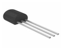
Package Type: TO-92
Max Drain to Source Voltage: 25 V
Max Drain to Gate Voltage: 25 V
Max Gate to Source Voltage: -25 V
Max Continues Gate Current: 10 mA
Max Power Dissipation: 350 mW
Storage temperature range: -65 to +150 Centigrade
Low Noise & High Gain
Specifications
- TypeParameter
- Lifecycle Status
Lifecycle Status refers to the current stage of an electronic component in its product life cycle, indicating whether it is active, obsolete, or transitioning between these states. An active status means the component is in production and available for purchase. An obsolete status indicates that the component is no longer being manufactured or supported, and manufacturers typically provide a limited time frame for support. Understanding the lifecycle status is crucial for design engineers to ensure continuity and reliability in their projects.
OBSOLETE (Last Updated: 1 day ago) - Mount
In electronic components, the term "Mount" typically refers to the method or process of physically attaching or fixing a component onto a circuit board or other electronic device. This can involve soldering, adhesive bonding, or other techniques to secure the component in place. The mounting process is crucial for ensuring proper electrical connections and mechanical stability within the electronic system. Different components may have specific mounting requirements based on their size, shape, and function, and manufacturers provide guidelines for proper mounting procedures to ensure optimal performance and reliability of the electronic device.
Through Hole - Package / Case
refers to the protective housing that encases an electronic component, providing mechanical support, electrical connections, and thermal management.
TO-92 - Number of Pins3
- Weight201mg
- Number of Elements1
- Power Dissipation (Max)350mW
- Packaging
Semiconductor package is a carrier / shell used to contain and cover one or more semiconductor components or integrated circuits. The material of the shell can be metal, plastic, glass or ceramic.
Bulk - JESD-609 Code
The "JESD-609 Code" in electronic components refers to a standardized marking code that indicates the lead-free solder composition and finish of electronic components for compliance with environmental regulations.
e0 - Pbfree Code
The "Pbfree Code" parameter in electronic components refers to the code or marking used to indicate that the component is lead-free. Lead (Pb) is a toxic substance that has been widely used in electronic components for many years, but due to environmental concerns, there has been a shift towards lead-free alternatives. The Pbfree Code helps manufacturers and users easily identify components that do not contain lead, ensuring compliance with regulations and promoting environmentally friendly practices. It is important to pay attention to the Pbfree Code when selecting electronic components to ensure they meet the necessary requirements for lead-free applications.
no - Number of Terminations3
- Terminal Finish
Terminal Finish refers to the surface treatment applied to the terminals or leads of electronic components to enhance their performance and longevity. It can improve solderability, corrosion resistance, and overall reliability of the connection in electronic assemblies. Common finishes include nickel, gold, and tin, each possessing distinct properties suitable for various applications. The choice of terminal finish can significantly impact the durability and effectiveness of electronic devices.
Tin/Lead (Sn/Pb) - Max Operating Temperature
The Maximum Operating Temperature is the maximum body temperature at which the thermistor is designed to operate for extended periods of time with acceptable stability of its electrical characteristics.
155°C - Min Operating Temperature
The "Min Operating Temperature" parameter in electronic components refers to the lowest temperature at which the component is designed to operate effectively and reliably. This parameter is crucial for ensuring the proper functioning and longevity of the component, as operating below this temperature may lead to performance issues or even damage. Manufacturers specify the minimum operating temperature to provide guidance to users on the environmental conditions in which the component can safely operate. It is important to adhere to this parameter to prevent malfunctions and ensure the overall reliability of the electronic system.
-55°C - HTS Code
HTS (Harmonized Tariff Schedule) codes are product classification codes between 8-1 digits. The first six digits are an HS code, and the countries of import assign the subsequent digits to provide additional classification. U.S. HTS codes are 1 digits and are administered by the U.S. International Trade Commission.
8541.21.00.95 - Voltage - Rated DC
Voltage - Rated DC is a parameter that specifies the maximum direct current (DC) voltage that an electronic component can safely handle without being damaged. This rating is crucial for ensuring the proper functioning and longevity of the component in a circuit. Exceeding the rated DC voltage can lead to overheating, breakdown, or even permanent damage to the component. It is important to carefully consider this parameter when designing or selecting components for a circuit to prevent any potential issues related to voltage overload.
25V - Terminal Position
In electronic components, the term "Terminal Position" refers to the physical location of the connection points on the component where external electrical connections can be made. These connection points, known as terminals, are typically used to attach wires, leads, or other components to the main body of the electronic component. The terminal position is important for ensuring proper connectivity and functionality of the component within a circuit. It is often specified in technical datasheets or component specifications to help designers and engineers understand how to properly integrate the component into their circuit designs.
BOTTOM - Peak Reflow Temperature (Cel)
Peak Reflow Temperature (Cel) is a parameter that specifies the maximum temperature at which an electronic component can be exposed during the reflow soldering process. Reflow soldering is a common method used to attach electronic components to a circuit board. The Peak Reflow Temperature is crucial because it ensures that the component is not damaged or degraded during the soldering process. Exceeding the specified Peak Reflow Temperature can lead to issues such as component failure, reduced performance, or even permanent damage to the component. It is important for manufacturers and assemblers to adhere to the recommended Peak Reflow Temperature to ensure the reliability and functionality of the electronic components.
240 - Current Rating
Current rating is the maximum current that a fuse will carry for an indefinite period without too much deterioration of the fuse element.
10mA - Time@Peak Reflow Temperature-Max (s)
Time@Peak Reflow Temperature-Max (s) refers to the maximum duration that an electronic component can be exposed to the peak reflow temperature during the soldering process, which is crucial for ensuring reliable solder joint formation without damaging the component.
30 - Pin Count
a count of all of the component leads (or pins)
3 - Qualification Status
An indicator of formal certification of qualifications.
Not Qualified - Element Configuration
The distribution of electrons of an atom or molecule (or other physical structure) in atomic or molecular orbitals.
Single - Operating Mode
A phase of operation during the operation and maintenance stages of the life cycle of a facility.
DEPLETION MODE - Power Dissipation
the process by which an electronic or electrical device produces heat (energy loss or waste) as an undesirable derivative of its primary action.
350mW - Transistor Application
In the context of electronic components, the parameter "Transistor Application" refers to the specific purpose or function for which a transistor is designed and used. Transistors are semiconductor devices that can amplify or switch electronic signals and are commonly used in various electronic circuits. The application of a transistor can vary widely depending on its design and characteristics, such as whether it is intended for audio amplification, digital logic, power control, or radio frequency applications. Understanding the transistor application is important for selecting the right type of transistor for a particular circuit or system to ensure optimal performance and functionality.
AMPLIFIER - Drain to Source Voltage (Vdss)
The Drain to Source Voltage (Vdss) is a key parameter in electronic components, particularly in field-effect transistors (FETs) such as MOSFETs. It refers to the maximum voltage that can be applied between the drain and source terminals of the FET without causing damage to the component. Exceeding this voltage limit can lead to breakdown and potentially permanent damage to the device.Vdss is an important specification to consider when designing or selecting components for a circuit, as it determines the operating range and reliability of the FET. It is crucial to ensure that the Vdss rating of the component is higher than the maximum voltage expected in the circuit to prevent failures and ensure proper functionality.In summary, the Drain to Source Voltage (Vdss) is a critical parameter that defines the maximum voltage tolerance of a FET component and plays a significant role in determining the overall performance and reliability of electronic circuits.
15V - Polarity/Channel Type
In electronic components, the parameter "Polarity/Channel Type" refers to the characteristic that determines the direction of current flow or the type of signal that can be accommodated by the component. For components like diodes and transistors, polarity indicates the direction in which current can flow through the component, such as forward bias or reverse bias for diodes. For components like MOSFETs or JFETs, the channel type refers to whether the component is an N-channel or P-channel device, which determines the type of charge carriers that carry current through the component. Understanding the polarity or channel type of a component is crucial for proper circuit design and ensuring that the component is connected correctly to achieve the desired functionality.
N-CHANNEL - Continuous Drain Current (ID)
Continuous Drain Current (ID) is a key parameter in electronic components, particularly in field-effect transistors (FETs) such as MOSFETs. It refers to the maximum current that can flow continuously through the drain terminal of the FET without causing damage to the component. This parameter is crucial for determining the power handling capability of the FET and is specified by the manufacturer in the component's datasheet. Designers must ensure that the actual operating current does not exceed the specified Continuous Drain Current to prevent overheating and potential failure of the component.
20mA - Gate to Source Voltage (Vgs)
The Gate to Source Voltage (Vgs) is a crucial parameter in electronic components, particularly in field-effect transistors (FETs) such as MOSFETs. It refers to the voltage difference between the gate and source terminals of the FET. This voltage determines the conductivity of the FET and controls the flow of current through the device. By varying the Vgs, the FET can be switched on or off, allowing for precise control of electronic circuits. Understanding and properly managing the Vgs is essential for ensuring the reliable and efficient operation of FET-based circuits.
-25V - Drain to Source Breakdown Voltage
Drain to Source Breakdown Voltage, often denoted as V(BR) D-S, is a critical parameter in electronic components, particularly in field-effect transistors (FETs) and metal-oxide-semiconductor FETs (MOSFETs). It represents the maximum voltage that can be applied between the drain and source terminals of the device without causing breakdown or permanent damage. Exceeding this voltage can lead to excessive current flow, resulting in thermal failure or destruction of the component. It is essential for ensuring reliable operation in circuit designs where high voltages may be encountered.
25V - FET Technology
Field-Effect Transistor (FET) technology is a type of semiconductor device commonly used in electronic components such as transistors and integrated circuits. FETs operate by controlling the flow of current through a semiconductor channel using an electric field. There are several types of FETs, including Metal-Oxide-Semiconductor FETs (MOSFETs) and Junction FETs (JFETs), each with its own characteristics and applications. FET technology offers advantages such as high input impedance, low power consumption, and fast switching speeds, making it suitable for a wide range of electronic devices and circuits. Overall, FET technology plays a crucial role in modern electronics by enabling efficient and reliable signal processing and amplification.
JUNCTION - Highest Frequency Band
The parameter "Highest Frequency Band" in electronic components refers to the range of frequencies within which the component can effectively operate or respond. It indicates the upper limit of the frequency range that the component can handle without significant degradation in performance. This parameter is particularly important in high-frequency applications such as RF (radio frequency) circuits and communication systems, where components need to be able to process signals within specific frequency bands. Understanding the highest frequency band of a component is crucial for ensuring proper functionality and compatibility within a given electronic system.
VERY HIGH FREQUENCY B - Height4.58mm
- Length4.58mm
- Width3.86mm
- RoHS Status
RoHS means “Restriction of Certain Hazardous Substances” in the “Hazardous Substances Directive” in electrical and electronic equipment.
RoHS Compliant - Lead Free
Lead Free is a term used to describe electronic components that do not contain lead as part of their composition. Lead is a toxic material that can have harmful effects on human health and the environment, so the electronics industry has been moving towards lead-free components to reduce these risks. Lead-free components are typically made using alternative materials such as silver, copper, and tin. Manufacturers must comply with regulations such as the Restriction of Hazardous Substances (RoHS) directive to ensure that their products are lead-free and environmentally friendly.
Lead Free
MPF102 Equivalents
BF245C, BF245B, 2N5457, 2N5458, NTE457, J113, 2N3819, 2N4416, NTE312, 2N5638, 2N5640, 2SK162, 2SK518
Please check the pin configuration and parameters before replacing them in your circuit.
Where to use MPF102
The MPF102 can be used in various amplification and switching applications. Its high gain and low noise features make it ideal to be used for the amplification of very small signals. The MPF102 can be used in signal booster circuits, audio preamplifier circuits, and audio amplifier stages, etc. As a switch, the MPF102 can be used to drive loads under 10mA such as in low ON resistance analog switching.
How to use MPF102
A JEFT is considered "ON" by default, that is even if there is no voltage applied to its gate and source terminals, the JFET will still allow current to flow from Drain to Source. In order to stop the JEFT from conducting current, a negative gate voltage has to be applied to the gate pin, for the MPF102 it should be typically -7.5V.

The images above showed how a load (LED) can be toggled using a JFET like MPF102. When the gate pin is grounded, the JFET allows current to flow from Drain to Source, and thus the LED is turned on. When it is biased using -7.5V on the gate pin, the JFET blocks the flow of current between the Drain and Source pin and thus turns off the LED.
MPF102 Applications
VHF signal amplifier
Low-level signal amplifier
Audio preamplifiers
Sensor circuits
Audio amplifier stages
Audio noise cancellation
Low ON resistance analog switching
MPF102 Package

MPF102 Package Outline

MPF102 Mechanical Data
MPF102 Manufacturer
ON Semiconductor (Nasdaq: ON) is driving energy-efficient innovations, empowering customers to reduce global energy use. The company offers a comprehensive portfolio of energy-efficient power and signal management, logic, discrete and custom solutions to help design engineers solve their unique design challenges in automotive, communications, computing, consumer, industrial, LED lighting, medical, military/aerospace, and power supply applications. ON Semiconductor operates a responsive, reliable, world-class supply chain and quality program, and a network of manufacturing facilities, sales offices, and design centers in key markets throughout North America, Europe, and the Asia Pacific regions.
Datasheet PDF
- Datasheets :
- ReachStatement :
1.What is MPF102?
The MPF102 is a JFET that has been used in many amplification circuits because of its low price. The JFET is currently no longer in production but the demand for it has created many clones in the market.
2.How to safely long run MPF102 in a circuit?
For a good circuit design, it is always essential to use all the components without giving them stress or don’t use them on their maximum ratings. To get the long-term stability of a component in a circuit it is recommended to always stay 20% below the max ratings. This same method will apply to the MPF102 transistor. Do not drive a load of more than 25V and 10mA, do not apply a reverse gate to source voltage of more than -25V, and always store or operate this transistor in temperature above -65 centigrade and below +150 centigrade.
3.What is the difference between MOSFET and JFET?
JFET (Junction Gate Field-Effect Transistor) is a three-terminal semiconductor device. MOSFET (Metal - Oxide - Semiconductor Field-Effect Transistor) is a four-terminal semiconductor device. It can only operate in depletion mode. It offers even higher input impedance than the JFETs, therefore they are more resistive.
4.How does a JFET work?
The junction-gate field-effect transistor (JFET) is one of the simplest types of field-effect transistor. Unlike bipolar junction transistors, JFETs are exclusively voltage-controlled in that they do not need a biasing current. Electric charge flows through a semiconducting channel between source and drain terminals.
5.Is JFET and FET same?
FET is categorized into JFET (Junction Field Effect Transistor) and MOSFET (Metal Oxide Semiconductor Field Effect Transistor). Both are mainly used in integrated circuits and are quite similar in operating principles, but they have a slightly different composition.
 A Comprehensive Guide to S-24CS64A0I-J8T1G EEPROM Memory Module
07 March 2024431
 BSS84 Transistor: Features, Pinout, and Datasheet
09 October 20212940
 AD9361 RF Agile Transceiver: 70 MHz to 6.0 GHz RF Chip, AD9361 CSPBGA and Datasheet
08 January 20226952
 ITR2010:Through Hole Photointerrupters - Slot Type - Transistor Output ROHS
08 January 20221936
 1N914 Diode: Alternatives, Features and Datasheet
09 August 20218560
 2N5486 Transistor: 2N5486 vs. MPF102, Equivalent, Datasheet
18 April 20224648
 MPU6000 Sensor: Comparison, Pinout, and Datasheet
10 December 202117079
 STM8L101 Microcontroller Series: A Comprehensive Technical Analysis
29 February 2024146
 Top 10 IC Design Companies in China
13 January 20229208
 What is Semiconductor Package?
06 December 202111522
 Demand for Automotive Chips Will Surge 300%
09 April 20225218
 What Makes a CPU?
30 March 20221621
 3-D Printing as Part of the Next Industrial Revolution
15 November 20191586
 Advancements and Challenges of High Frequency Converters
19 June 20231943
 L298N: A Motor Driver That Accepts High Voltages
24 February 20234366
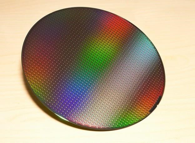 Analysis of Semiconductor Wafers
22 October 202515024
ON Semiconductor
In Stock: 200215
United States
China
Canada
Japan
Russia
Germany
United Kingdom
Singapore
Italy
Hong Kong(China)
Taiwan(China)
France
Korea
Mexico
Netherlands
Malaysia
Austria
Spain
Switzerland
Poland
Thailand
Vietnam
India
United Arab Emirates
Afghanistan
Åland Islands
Albania
Algeria
American Samoa
Andorra
Angola
Anguilla
Antigua & Barbuda
Argentina
Armenia
Aruba
Australia
Azerbaijan
Bahamas
Bahrain
Bangladesh
Barbados
Belarus
Belgium
Belize
Benin
Bermuda
Bhutan
Bolivia
Bonaire, Sint Eustatius and Saba
Bosnia & Herzegovina
Botswana
Brazil
British Indian Ocean Territory
British Virgin Islands
Brunei
Bulgaria
Burkina Faso
Burundi
Cabo Verde
Cambodia
Cameroon
Cayman Islands
Central African Republic
Chad
Chile
Christmas Island
Cocos (Keeling) Islands
Colombia
Comoros
Congo
Congo (DRC)
Cook Islands
Costa Rica
Côte d’Ivoire
Croatia
Cuba
Curaçao
Cyprus
Czechia
Denmark
Djibouti
Dominica
Dominican Republic
Ecuador
Egypt
El Salvador
Equatorial Guinea
Eritrea
Estonia
Eswatini
Ethiopia
Falkland Islands
Faroe Islands
Fiji
Finland
French Guiana
French Polynesia
Gabon
Gambia
Georgia
Ghana
Gibraltar
Greece
Greenland
Grenada
Guadeloupe
Guam
Guatemala
Guernsey
Guinea
Guinea-Bissau
Guyana
Haiti
Honduras
Hungary
Iceland
Indonesia
Iran
Iraq
Ireland
Isle of Man
Israel
Jamaica
Jersey
Jordan
Kazakhstan
Kenya
Kiribati
Kosovo
Kuwait
Kyrgyzstan
Laos
Latvia
Lebanon
Lesotho
Liberia
Libya
Liechtenstein
Lithuania
Luxembourg
Macao(China)
Madagascar
Malawi
Maldives
Mali
Malta
Marshall Islands
Martinique
Mauritania
Mauritius
Mayotte
Micronesia
Moldova
Monaco
Mongolia
Montenegro
Montserrat
Morocco
Mozambique
Myanmar
Namibia
Nauru
Nepal
New Caledonia
New Zealand
Nicaragua
Niger
Nigeria
Niue
Norfolk Island
North Korea
North Macedonia
Northern Mariana Islands
Norway
Oman
Pakistan
Palau
Palestinian Authority
Panama
Papua New Guinea
Paraguay
Peru
Philippines
Pitcairn Islands
Portugal
Puerto Rico
Qatar
Réunion
Romania
Rwanda
Samoa
San Marino
São Tomé & Príncipe
Saudi Arabia
Senegal
Serbia
Seychelles
Sierra Leone
Sint Maarten
Slovakia
Slovenia
Solomon Islands
Somalia
South Africa
South Sudan
Sri Lanka
St Helena, Ascension, Tristan da Cunha
St. Barthélemy
St. Kitts & Nevis
St. Lucia
St. Martin
St. Pierre & Miquelon
St. Vincent & Grenadines
Sudan
Suriname
Svalbard & Jan Mayen
Sweden
Syria
Tajikistan
Tanzania
Timor-Leste
Togo
Tokelau
Tonga
Trinidad & Tobago
Tunisia
Turkey
Turkmenistan
Turks & Caicos Islands
Tuvalu
U.S. Outlying Islands
U.S. Virgin Islands
Uganda
Ukraine
Uruguay
Uzbekistan
Vanuatu
Vatican City
Venezuela
Wallis & Futuna
Yemen
Zambia
Zimbabwe
![MMBFJ310LT1G]() MMBFJ310LT1G
MMBFJ310LT1GON Semiconductor
![MMBFJ309LT1G]() MMBFJ309LT1G
MMBFJ309LT1GON Semiconductor
![MMBF5484]() MMBF5484
MMBF5484ON Semiconductor
![2SK3557-6-TB-E]() 2SK3557-6-TB-E
2SK3557-6-TB-EON Semiconductor
![MMBF4416A]() MMBF4416A
MMBF4416AON Semiconductor
![MMBF5485]() MMBF5485
MMBF5485ON Semiconductor
![SMMBFJ310LT1G]() SMMBFJ310LT1G
SMMBFJ310LT1GON Semiconductor
![J310]() J310
J310ON Semiconductor
![MMBFJ211]() MMBFJ211
MMBFJ211ON Semiconductor
![MMBFJ309]() MMBFJ309
MMBFJ309ON Semiconductor


