

 Product
 Brand
Brand Articles
 Tools
Tools
IRF9640 P-Channel MOSFET: Pinout, Datasheet, Equivalent, and Circuit


P-Channel Tube 500mOhm @ 6.6A, 10V ±20V 1200pF @ 25V 44nC @ 10V 200V TO-220-3
The IRF9640 is a P-Channel enhancement mode silicon-gate power field-effect transistor.
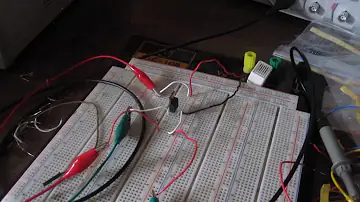
P Channel MOSFET Switch Circuit
IRF9640 Description
The IRF9640 is a P-Channel enhancement mode silicon-gate power field-effect transistor. It is an advanced power MOSFET designed, tested, and guaranteed to withstand a specified level of energy in the breakdown avalanche mode of operation. The IRF9640 is designed for applications such as switching regulators, switching converters, motor drivers, relay drivers, and as drivers for other high-power switching devices. The high input impedance allows the IRF9640 to be operated directly from integrated circuits.
IRF9640 Pinout

IRF9640 Pinout
IRF9640 CAD Model
Symbol
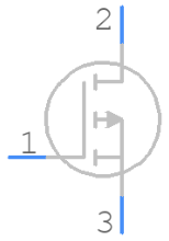
IRF9640 Symbol
Footprint
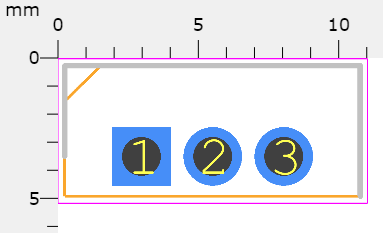
IRF9640 Footprint
3D Model
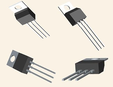
IRF9640 3D Model
IRF9640 Features
Transistor Type: P-Channel
Package Type: TO-220
Max Drain to Source Voltage: -200 V
Max Gate to Source Voltage: ±20 V
Max Continues Drain Current: -11 A
Drain to Source Resistance in ON State: 500 mΩ
Max Pulsed Drain Current: -44 A
Max Power Dissipation: 125W
Storage & Operating Temperature: -55 to +150 Centigrade
IRF9640 Advantages
Dynamic dV/dt Rating
Repetitive Avalanche Rated
P-Channel
Fast Switching
Ease of Paralleling
Simple Drive Requirements
Compliant to RoHS Directive 2002/95/EC
Specifications
- TypeParameter
- Mount
In electronic components, the term "Mount" typically refers to the method or process of physically attaching or fixing a component onto a circuit board or other electronic device. This can involve soldering, adhesive bonding, or other techniques to secure the component in place. The mounting process is crucial for ensuring proper electrical connections and mechanical stability within the electronic system. Different components may have specific mounting requirements based on their size, shape, and function, and manufacturers provide guidelines for proper mounting procedures to ensure optimal performance and reliability of the electronic device.
Through Hole - Mounting Type
The "Mounting Type" in electronic components refers to the method used to attach or connect a component to a circuit board or other substrate, such as through-hole, surface-mount, or panel mount.
Through Hole - Package / Case
refers to the protective housing that encases an electronic component, providing mechanical support, electrical connections, and thermal management.
TO-220-3 - Number of Pins3
- Supplier Device Package
The parameter "Supplier Device Package" in electronic components refers to the physical packaging or housing of the component as provided by the supplier. It specifies the form factor, dimensions, and layout of the component, which are crucial for compatibility and integration into electronic circuits and systems. The supplier device package information typically includes details such as the package type (e.g., DIP, SOP, QFN), number of pins, pitch, and overall size, allowing engineers and designers to select the appropriate component for their specific application requirements. Understanding the supplier device package is essential for proper component selection, placement, and soldering during the manufacturing process to ensure optimal performance and reliability of the electronic system.
TO-220AB - Weight6.000006g
- Current - Continuous Drain (Id) @ 25℃11A Tc
- Drive Voltage (Max Rds On, Min Rds On)10V
- Number of Elements1
- Power Dissipation (Max)125W Tc
- Turn Off Delay Time
It is the time from when Vgs drops below 90% of the gate drive voltage to when the drain current drops below 90% of the load current. It is the delay before current starts to transition in the load, and depends on Rg. Ciss.
39 ns - Operating Temperature
The operating temperature is the range of ambient temperature within which a power supply, or any other electrical equipment, operate in. This ranges from a minimum operating temperature, to a peak or maximum operating temperature, outside which, the power supply may fail.
-55°C~150°C TJ - Packaging
Semiconductor package is a carrier / shell used to contain and cover one or more semiconductor components or integrated circuits. The material of the shell can be metal, plastic, glass or ceramic.
Tube - Published2011
- Part Status
Parts can have many statuses as they progress through the configuration, analysis, review, and approval stages.
Obsolete - Moisture Sensitivity Level (MSL)
Moisture Sensitivity Level (MSL) is a standardized rating that indicates the susceptibility of electronic components, particularly semiconductors, to moisture-induced damage during storage and the soldering process, defining the allowable exposure time to ambient conditions before they require special handling or baking to prevent failures
1 (Unlimited) - Max Operating Temperature
The Maximum Operating Temperature is the maximum body temperature at which the thermistor is designed to operate for extended periods of time with acceptable stability of its electrical characteristics.
150°C - Min Operating Temperature
The "Min Operating Temperature" parameter in electronic components refers to the lowest temperature at which the component is designed to operate effectively and reliably. This parameter is crucial for ensuring the proper functioning and longevity of the component, as operating below this temperature may lead to performance issues or even damage. Manufacturers specify the minimum operating temperature to provide guidance to users on the environmental conditions in which the component can safely operate. It is important to adhere to this parameter to prevent malfunctions and ensure the overall reliability of the electronic system.
-55°C - Voltage - Rated DC
Voltage - Rated DC is a parameter that specifies the maximum direct current (DC) voltage that an electronic component can safely handle without being damaged. This rating is crucial for ensuring the proper functioning and longevity of the component in a circuit. Exceeding the rated DC voltage can lead to overheating, breakdown, or even permanent damage to the component. It is important to carefully consider this parameter when designing or selecting components for a circuit to prevent any potential issues related to voltage overload.
-200V - Current Rating
Current rating is the maximum current that a fuse will carry for an indefinite period without too much deterioration of the fuse element.
-11A - Number of Channels1
- Element Configuration
The distribution of electrons of an atom or molecule (or other physical structure) in atomic or molecular orbitals.
Single - Power Dissipation
the process by which an electronic or electrical device produces heat (energy loss or waste) as an undesirable derivative of its primary action.
125W - Turn On Delay Time
Turn-on delay, td(on), is the time taken to charge the input capacitance of the device before drain current conduction can start.
13 ns - FET Type
"FET Type" refers to the type of Field-Effect Transistor (FET) being used in an electronic component. FETs are three-terminal semiconductor devices that can be classified into different types based on their construction and operation. The main types of FETs include Metal-Oxide-Semiconductor FETs (MOSFETs), Junction FETs (JFETs), and Insulated-Gate Bipolar Transistors (IGBTs).Each type of FET has its own unique characteristics and applications. MOSFETs are commonly used in digital circuits due to their high input impedance and low power consumption. JFETs are often used in low-noise amplifiers and switching circuits. IGBTs combine the high input impedance of MOSFETs with the high current-carrying capability of bipolar transistors, making them suitable for high-power applications like motor control and power inverters.When selecting an electronic component, understanding the FET type is crucial as it determines the device's performance and suitability for a specific application. It is important to consider factors such as voltage ratings, current handling capabilities, switching speeds, and power dissipation when choosing the right FET type for a particular circuit design.
P-Channel - Rds On (Max) @ Id, Vgs
Rds On (Max) @ Id, Vgs refers to the maximum on-resistance of a MOSFET or similar transistor when it is fully turned on or in the saturation region. It is specified at a given drain current (Id) and gate-source voltage (Vgs). This parameter indicates how much resistance the component will offer when conducting, impacting power loss and efficiency in a circuit. Lower Rds On values are preferred for better performance in switching applications.
500mOhm @ 6.6A, 10V - Vgs(th) (Max) @ Id
The parameter "Vgs(th) (Max) @ Id" in electronic components refers to the maximum gate-source threshold voltage at a specified drain current (Id). This parameter is commonly found in field-effect transistors (FETs) and is used to define the minimum voltage required at the gate terminal to turn on the transistor and allow current to flow from the drain to the source. The maximum value indicates the upper limit of this threshold voltage under specified operating conditions. It is an important parameter for determining the proper biasing and operating conditions of the FET in a circuit to ensure proper functionality and performance.
4V @ 250μA - Input Capacitance (Ciss) (Max) @ Vds
The parameter "Input Capacitance (Ciss) (Max) @ Vds" in electronic components refers to the maximum input capacitance measured at a specific drain-source voltage (Vds). Input capacitance is a crucial parameter in field-effect transistors (FETs) and power MOSFETs, as it represents the total capacitance at the input terminal of the device. This capacitance affects the device's switching speed and overall performance, as it influences the time required for charging and discharging during operation. Manufacturers provide this parameter to help designers understand the device's input characteristics and make informed decisions when integrating it into a circuit.
1200pF @ 25V - Gate Charge (Qg) (Max) @ Vgs
Gate Charge (Qg) (Max) @ Vgs refers to the maximum amount of charge that must be supplied to the gate of a MOSFET or similar device to fully turn it on, measured at a specific gate-source voltage (Vgs). This parameter is crucial for understanding the switching characteristics of the device, as it influences the speed at which the gate can charge and discharge. A higher gate charge value often implies slower switching speeds, which can impact the efficiency of high-frequency applications. This parameter is typically specified in nanocoulombs (nC) in the component's datasheet.
44nC @ 10V - Rise Time
In electronics, when describing a voltage or current step function, rise time is the time taken by a signal to change from a specified low value to a specified high value.
43ns - Drain to Source Voltage (Vdss)
The Drain to Source Voltage (Vdss) is a key parameter in electronic components, particularly in field-effect transistors (FETs) such as MOSFETs. It refers to the maximum voltage that can be applied between the drain and source terminals of the FET without causing damage to the component. Exceeding this voltage limit can lead to breakdown and potentially permanent damage to the device.Vdss is an important specification to consider when designing or selecting components for a circuit, as it determines the operating range and reliability of the FET. It is crucial to ensure that the Vdss rating of the component is higher than the maximum voltage expected in the circuit to prevent failures and ensure proper functionality.In summary, the Drain to Source Voltage (Vdss) is a critical parameter that defines the maximum voltage tolerance of a FET component and plays a significant role in determining the overall performance and reliability of electronic circuits.
200V - Vgs (Max)
Vgs (Max) refers to the maximum gate-source voltage that can be applied to a field-effect transistor (FET) without causing damage to the component. This parameter is crucial in determining the safe operating limits of the FET and helps prevent overvoltage conditions that could lead to device failure. Exceeding the specified Vgs (Max) rating can result in breakdown of the gate oxide layer, leading to permanent damage to the FET. Designers must ensure that the applied gate-source voltage does not exceed the maximum rating to ensure reliable and long-term operation of the electronic component.
±20V - Fall Time (Typ)
Fall Time (Typ) is a parameter used to describe the time it takes for a signal to transition from a high level to a low level in an electronic component, such as a transistor or an integrated circuit. It is typically measured in nanoseconds or microseconds and is an important characteristic that affects the performance of the component in digital circuits. A shorter fall time indicates faster switching speeds and can result in improved overall circuit performance, such as reduced power consumption and increased data transmission rates. Designers often consider the fall time specification when selecting components for their circuits to ensure proper functionality and efficiency.
38 ns - Continuous Drain Current (ID)
Continuous Drain Current (ID) is a key parameter in electronic components, particularly in field-effect transistors (FETs) such as MOSFETs. It refers to the maximum current that can flow continuously through the drain terminal of the FET without causing damage to the component. This parameter is crucial for determining the power handling capability of the FET and is specified by the manufacturer in the component's datasheet. Designers must ensure that the actual operating current does not exceed the specified Continuous Drain Current to prevent overheating and potential failure of the component.
11A - Gate to Source Voltage (Vgs)
The Gate to Source Voltage (Vgs) is a crucial parameter in electronic components, particularly in field-effect transistors (FETs) such as MOSFETs. It refers to the voltage difference between the gate and source terminals of the FET. This voltage determines the conductivity of the FET and controls the flow of current through the device. By varying the Vgs, the FET can be switched on or off, allowing for precise control of electronic circuits. Understanding and properly managing the Vgs is essential for ensuring the reliable and efficient operation of FET-based circuits.
20V - Input Capacitance
The capacitance between the input terminals of an op amp with either input grounded. It is expressed in units of farads.
1.2nF - Drain to Source Resistance
The Drain to Source Resistance, often denoted as RDS(on), is a crucial parameter in electronic components, particularly in field-effect transistors (FETs) such as MOSFETs. It represents the resistance between the drain and source terminals when the FET is in its on-state, conducting current. A lower RDS(on) value indicates better conductivity and efficiency, as it results in less power dissipation and heat generation in the component. Designers often aim to minimize RDS(on) to improve the performance and overall efficiency of electronic circuits, especially in power applications where minimizing losses is critical.
500mOhm - Rds On Max
Rds On Max refers to the maximum on-state resistance of a MOSFET (Metal-Oxide-Semiconductor Field-Effect Transistor) when it is fully conducting. This parameter indicates the resistance that the MOSFET presents when it is in the ON state, allowing current to flow through. A lower Rds On Max value indicates that the MOSFET can conduct more current with less resistance, leading to higher efficiency and lower power dissipation. Designers often look for MOSFETs with a lower Rds On Max value to minimize power losses and improve overall performance in electronic circuits.
500 mΩ - Height9.01mm
- Length10.41mm
- Width4.7mm
- RoHS Status
RoHS means “Restriction of Certain Hazardous Substances” in the “Hazardous Substances Directive” in electrical and electronic equipment.
Non-RoHS Compliant - Lead Free
Lead Free is a term used to describe electronic components that do not contain lead as part of their composition. Lead is a toxic material that can have harmful effects on human health and the environment, so the electronics industry has been moving towards lead-free components to reduce these risks. Lead-free components are typically made using alternative materials such as silver, copper, and tin. Manufacturers must comply with regulations such as the Restriction of Hazardous Substances (RoHS) directive to ensure that their products are lead-free and environmentally friendly.
Contains Lead
IRF9640 Test Circuits

IRF9640 Unclamped Energy Test Circuit and Waveforms

IRF9640 Switching Time Test Circuit and Waveforms

IRF9640 Gate Charge Test Circuit and Waveforms
IRF9640 Alternatives
| Part Number | Description | Manufacturer |
| IRF9640 TRANSISTORS | 11A, 200V, 0.5ohm, P-CHANNEL, Si, POWER, MOSFET, TO-220AB | Rochester Electronics LLC |
| IRF9640-009 TRANSISTORS | Power Field-Effect Transistor, 11A I(D), 200V, 0.5ohm, 1-Element, P-Channel, Silicon, Metal-oxide Semiconductor FET, TO-220AB | Vishay Intertechnologies |
| IRF9640-001 TRANSISTORS | Power Field-Effect Transistor, 11A I(D), 200V, 0.5ohm, 1-Element, P-Channel, Silicon, Metal-oxide Semiconductor FET | International Rectifier |
| IRF9640-010 TRANSISTORS | Power Field-Effect Transistor, 11A I(D), 200V, 0.5ohm, 1-Element, P-Channel, Silicon, Metal-oxide Semiconductor FET, TO-220AB | International Rectifier |
| IRF9640-006 TRANSISTORS | Power Field-Effect Transistor, 11A I(D), 200V, 0.5ohm, 1-Element, P-Channel, Silicon, Metal-oxide Semiconductor FET, TO-220AB | Vishay Intertechnologies |
| IRF9640PBF TRANSISTORS | Power Field-Effect Transistor, 11A I(D), 200V, 0.5ohm, 1-Element, P-Channel, Silicon, Metal-oxide Semiconductor FET, TO-220AB, ROHS COMPLIANT PACKAGE-3 | Vishay Intertechnologies |
IRF9640 Equivalents
2SJ513, CEP14P20, IRF9640PBF, 9640S, IRFP9240, MTW14P20, IRF044, IRF044SMD, IRF054, IRF054SMD, IRF100B201, IRF100B202
Please check the pin configuration and parameters before replacing them in your circuit.
Where to use IRF9640
The IRF9640 is a P-Channel MOSFET manufactured in the TO-220 package. The continuous drain current of the IRF9640 is -11A therefore you can drive a maximum load of -11A through the MOSFET with a maximum load voltage of -200V. The IRF9640 can be used in a variety of switching and amplification applications. It is capable of delivering fast switching speed hence can be used in applications where fast switching is needed. With a drain to source resistance as low as 500 mΩ, less power is wasted hence improves efficiency. Moreover, the IRF9640 has low driving requirements which makes it capable of operating directly from ICs, microcontrollers, and electronic platforms such as Arduino.
IRF9640 Applications
Switching Regulators
Switching Converters
Uninterrupted Power Supplies
Battery Chargers
Solar Applications
Motor Drivers
Relay Drivers
IRF9640 Package
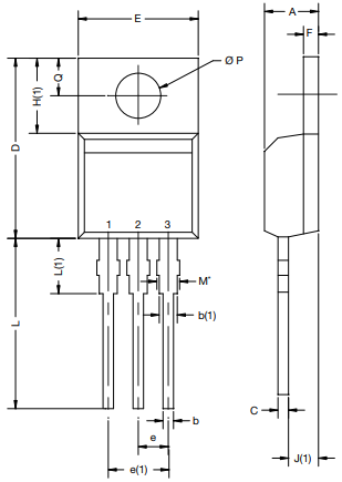
IRF9640 Package Outline
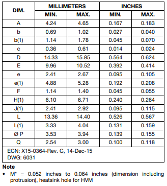
IRF9640 Mechanical Data
IRF9640 Manufacturer
Vishay, through its Siliconix subsidiary, leads the industry in the development of power semiconductor products that improve the efficiency of power management circuitry in end products while reducing space requirements. As the world's number-one brand of low-voltage power MOSFETs (metal-oxide-semiconductor field-effect transistors), Vishay Siliconix products play a key role in making handheld and portable electronic systems operate more efficiently from smaller and lighter battery packs.
Datasheet PDF
- Datasheets :
- Other Related Documents :
- RohsStatement :
- PCN Obsolescence/ EOL :
Parts with Similar Specs
- ImagePart NumberManufacturerMountPackage / CaseDrain to Source Voltage (Vdss)Continuous Drain Current (ID)Current - Continuous Drain (Id) @ 25°CRds On MaxGate to Source Voltage (Vgs)Power DissipationPower Dissipation-MaxView Compare
![IRF9640]()
IRF9640
Through Hole
TO-220-3
200V
11 A
11A (Tc)
500 mΩ
20 V
125 W
125W (Tc)
![FQPF10N20C]()
Through Hole
TO-220-3 Full Pack
-
9.5 A
9.5A (Tc)
-
30 V
38 W
38W (Tc)
![IRF630FP]()
Through Hole
TO-220-3 Full Pack
-
9.8 A
9.8A (Tc)
-
20 V
40 W
40W (Tc)
![IRLS640A]()
Through Hole
TO-220-3 Full Pack, Isolated Tab
200V
9.8 A
9.8A (Tc)
180 mΩ
20 V
40 W
40W (Tc)


1.What is IRF9640?
The IRF9640 is a P-Channel enhancement mode silicon-gate power field-effect transistor. It is an advanced power MOSFET designed, tested, and guaranteed to withstand a specified level of energy in the breakdown avalanche mode of operation.
2.How to safely long run IRF9640 in a circuit?
For long-term performance with this device use it 20% below its maximum ratings. The maximum continuous drain current -11A, therefore, does not drive a load of more than -8.8A. The maximum drain to source voltage is -200V therefore do not drive a load of more than -160V, use a suitable heatsink with this transistor and always store or operate the transistor at a temperature above -55 degrees Celsius and below +150 degrees Celsius.
3.What is P-channel MOSFET used for?
P-channel MOSFETs are often used for load switching. The simplicity of P-channel solutions on the high side makes them equally attractive for applications such as Low-Voltage Drives and non-isolated Point of Loads in systems where space is at a premium.
4.What is P-channel enhancement MOSFET?
P-Channel MOSFET is a classification of Metal Oxide Semiconductor Device. This consists of the n-substrate in the middle with a light doping concentration. These are the three terminals devices. It possesses uni-polar characteristics because its operation is dependent on the majority of the charge carriers.
 LPS53 Open Frame AC DC Converters Output 12V: Datasheet, Features, and LPS53 VS NPS63-M-006
12 April 2022633
 TSL2591 Converter: Datasheet, Pinout and Schematic
18 August 20213036
 ATTINY85-20SU Microcontroller: Circuit, Pinout, and Datasheet
21 February 20225600
 MIC2545A Programmable Current-Limit High-Side Switch: Pinout, Equivalent and Datasheet
29 March 2022655
 AD9516-4 Clock Generator: Pinout, Equivalent and Datasheet
09 April 2022438
 CP2102 Bridge Driver: Alternative, Pinout and Datasheet
14 July 202111376
 ADS1262 ADC: Feature, Pinout and Datasheet
16 August 20247221
 STM32F302RBT7 Microcontroller: 32-Bit, 64-LQFP, Pinout and Features
18 January 2022775
 A Hybrid SiC and GaN-Based DC-DC Converter for EVs
20 September 20242891
 Understanding Photodiodes: Working Principles and Applications - Part 2
24 May 20245093
 GenAI Boosts Semiconductor Market with First Revenue Increase in Five Quarters
25 March 20244141
 Introduction to UFS (Universal Flash Storage)
23 July 20218542
 What is a Digital Potentiometer?
08 January 20268782
 What is an Operational Amplifier?
27 March 20253894
 Revolutionizing Semiconductor Manufacturing with New Plasma Power Technologies
23 September 20232361
 Introduction to Wireless Sensor Networks
20 August 20204854
Vishay Siliconix
In Stock
United States
China
Canada
Japan
Russia
Germany
United Kingdom
Singapore
Italy
Hong Kong(China)
Taiwan(China)
France
Korea
Mexico
Netherlands
Malaysia
Austria
Spain
Switzerland
Poland
Thailand
Vietnam
India
United Arab Emirates
Afghanistan
Åland Islands
Albania
Algeria
American Samoa
Andorra
Angola
Anguilla
Antigua & Barbuda
Argentina
Armenia
Aruba
Australia
Azerbaijan
Bahamas
Bahrain
Bangladesh
Barbados
Belarus
Belgium
Belize
Benin
Bermuda
Bhutan
Bolivia
Bonaire, Sint Eustatius and Saba
Bosnia & Herzegovina
Botswana
Brazil
British Indian Ocean Territory
British Virgin Islands
Brunei
Bulgaria
Burkina Faso
Burundi
Cabo Verde
Cambodia
Cameroon
Cayman Islands
Central African Republic
Chad
Chile
Christmas Island
Cocos (Keeling) Islands
Colombia
Comoros
Congo
Congo (DRC)
Cook Islands
Costa Rica
Côte d’Ivoire
Croatia
Cuba
Curaçao
Cyprus
Czechia
Denmark
Djibouti
Dominica
Dominican Republic
Ecuador
Egypt
El Salvador
Equatorial Guinea
Eritrea
Estonia
Eswatini
Ethiopia
Falkland Islands
Faroe Islands
Fiji
Finland
French Guiana
French Polynesia
Gabon
Gambia
Georgia
Ghana
Gibraltar
Greece
Greenland
Grenada
Guadeloupe
Guam
Guatemala
Guernsey
Guinea
Guinea-Bissau
Guyana
Haiti
Honduras
Hungary
Iceland
Indonesia
Iran
Iraq
Ireland
Isle of Man
Israel
Jamaica
Jersey
Jordan
Kazakhstan
Kenya
Kiribati
Kosovo
Kuwait
Kyrgyzstan
Laos
Latvia
Lebanon
Lesotho
Liberia
Libya
Liechtenstein
Lithuania
Luxembourg
Macao(China)
Madagascar
Malawi
Maldives
Mali
Malta
Marshall Islands
Martinique
Mauritania
Mauritius
Mayotte
Micronesia
Moldova
Monaco
Mongolia
Montenegro
Montserrat
Morocco
Mozambique
Myanmar
Namibia
Nauru
Nepal
New Caledonia
New Zealand
Nicaragua
Niger
Nigeria
Niue
Norfolk Island
North Korea
North Macedonia
Northern Mariana Islands
Norway
Oman
Pakistan
Palau
Palestinian Authority
Panama
Papua New Guinea
Paraguay
Peru
Philippines
Pitcairn Islands
Portugal
Puerto Rico
Qatar
Réunion
Romania
Rwanda
Samoa
San Marino
São Tomé & Príncipe
Saudi Arabia
Senegal
Serbia
Seychelles
Sierra Leone
Sint Maarten
Slovakia
Slovenia
Solomon Islands
Somalia
South Africa
South Sudan
Sri Lanka
St Helena, Ascension, Tristan da Cunha
St. Barthélemy
St. Kitts & Nevis
St. Lucia
St. Martin
St. Pierre & Miquelon
St. Vincent & Grenadines
Sudan
Suriname
Svalbard & Jan Mayen
Sweden
Syria
Tajikistan
Tanzania
Timor-Leste
Togo
Tokelau
Tonga
Trinidad & Tobago
Tunisia
Turkey
Turkmenistan
Turks & Caicos Islands
Tuvalu
U.S. Outlying Islands
U.S. Virgin Islands
Uganda
Ukraine
Uruguay
Uzbekistan
Vanuatu
Vatican City
Venezuela
Wallis & Futuna
Yemen
Zambia
Zimbabwe

