
 Product
 Brand
Brand Articles
 Tools
Tools
AD9516-4 Clock Generator: Pinout, Equivalent and Datasheet

3.3V Clock Generator, Fanout Distribution AD9516 Clock Generators 64 Pins 64-VFQFN Exposed Pad, CSP 64 Terminals Surface Mount 3.135V~3.465V Tape & Reel (TR)
Unit Price: $22.557888
Ext Price: $22.56


3.3V Clock Generator, Fanout Distribution AD9516 Clock Generators 64 Pins 64-VFQFN Exposed Pad, CSP 64 Terminals Surface Mount 3.135V~3.465V Tape & Reel (TR)
The AD9516-4 provides a multi-output clock distribution function with subpicosecond jitter performance, along with an on-chip PLL and VCO. The AD9516-4 emphasizes low jitter and phase noise to maximize data converter performance, and it can benefit other applications with demanding phase noise and jitter requirements. Furthermore, Huge range of Semiconductors, Capacitors, Resistors and IcS in stock. Welcome RFQ.

What is CLOCK GENERATOR? What does CLOCK GENERATOR mean? CLOCK GENERATOR meaning & explanation
AD9516-4 Pinout
The following figure is the diagram of AD9516-4 Pinout.

Pinout
AD9516-4 CAD Model
The following figure is the diagram of AD9516-4 Footprint.

Footprint
AD9516-4 Description
The AD9516-4 provides a multi-output clock distribution function with subpicosecond jitter performance, along with an on-chip PLL and VCO. The on-chip VCO tunes from 1.45 GHz to 1.80 GHz. Optionally, an external VCO/VCXO of up to 2.4 GHz can be used. The AD9516-4 emphasizes low jitter and phase noise to maximize data converter performance, and it can benefit other applications with demanding phase noise and jitter requirements. The AD9516-4 features six LVPECL outputs (in three pairs) and four LVDS outputs (in two pairs). Each LVDS output can be reconfigured as two CMOS outputs. The LVPECL outputs operate to 1.6 GHz, the LVDS outputs operate to 800 MHz, and the CMOS outputs operate to 250 MHz. Each pair of outputs has dividers that allow both the divide ratio and coarse delay (or phase) to be set. The range of division for the LVPECL outputs is 1 to 32. The LVDS/CMOS outputs allow a range of divisions, up to a maximum of 1024.
The AD9516-4 is available in a 64-lead LFCSP and can be operated from a single 3.3 V supply. An external VCO, which requires an extended voltage range, can be accommodated by connecting the charge pump supply (VCP to 5 V. A separate LVPECL power supply can be from 2.5 V to 3.3 V (nominal). The AD9516-4 is specified for operation over the industrial range of −40°C to +85°C.
This article will introduce AD9516-4 systematically from its features, pinout to its specifications, applications, also including AD9516-4 datasheet and so much more.
AD9516-4 Features
● Low phase noise, phase-locked loop (PLL)
● On-chip VCO tunes from 1.45 GHz to 1.80 GHz
● External VCO/VCXO to 2.4 GHz optional
● 1 differential or 2 single-ended reference inputs
● Reference monitoring capability
● Automatic revertive and manual reference switchover/holdover modes
● Accepts LVPECL, LVDS, or CMOS references to 250 MHz
● Programmable delays in path to PFD
● Digital or analog lock detect, selectable
● 6 pairs of 1.6 GHz LVPECL outputs
● Each output pair shares a 1-to-32 divider with coarse phase delay
● Additive output jitter: 225 fs rms
● Channel-to-channel skew paired outputs of <10 ps
● 4 pairs of 800 MHz LVDS clock outputs
● Each output pair shares two cascaded 1-to-32 dividers with coarse phase delay
● Additive output jitter: 275 fs rms
● Fine delay adjust (Δt) on each LVDS output
● Each LVDS output can be reconfigured as two 250 MHz CMOS outputs
● Automatic synchronization of all outputs on power-up
● Manual output synchronization available
● 64-lead LFCSP
Specifications
- TypeParameter
- Lifecycle Status
Lifecycle Status refers to the current stage of an electronic component in its product life cycle, indicating whether it is active, obsolete, or transitioning between these states. An active status means the component is in production and available for purchase. An obsolete status indicates that the component is no longer being manufactured or supported, and manufacturers typically provide a limited time frame for support. Understanding the lifecycle status is crucial for design engineers to ensure continuity and reliability in their projects.
PRODUCTION (Last Updated: 4 weeks ago) - Factory Lead Time8 Weeks
- Contact Plating
Contact plating (finish) provides corrosion protection for base metals and optimizes the mechanical and electrical properties of the contact interfaces.
Tin - Mounting Type
The "Mounting Type" in electronic components refers to the method used to attach or connect a component to a circuit board or other substrate, such as through-hole, surface-mount, or panel mount.
Surface Mount - Package / Case
refers to the protective housing that encases an electronic component, providing mechanical support, electrical connections, and thermal management.
64-VFQFN Exposed Pad, CSP - Surface Mount
having leads that are designed to be soldered on the side of a circuit board that the body of the component is mounted on.
YES - Number of Pins64
- Frequency(Max)2.95GHz
- Operating Temperature
The operating temperature is the range of ambient temperature within which a power supply, or any other electrical equipment, operate in. This ranges from a minimum operating temperature, to a peak or maximum operating temperature, outside which, the power supply may fail.
-40°C~85°C - Packaging
Semiconductor package is a carrier / shell used to contain and cover one or more semiconductor components or integrated circuits. The material of the shell can be metal, plastic, glass or ceramic.
Tape & Reel (TR) - JESD-609 Code
The "JESD-609 Code" in electronic components refers to a standardized marking code that indicates the lead-free solder composition and finish of electronic components for compliance with environmental regulations.
e3 - Pbfree Code
The "Pbfree Code" parameter in electronic components refers to the code or marking used to indicate that the component is lead-free. Lead (Pb) is a toxic substance that has been widely used in electronic components for many years, but due to environmental concerns, there has been a shift towards lead-free alternatives. The Pbfree Code helps manufacturers and users easily identify components that do not contain lead, ensuring compliance with regulations and promoting environmentally friendly practices. It is important to pay attention to the Pbfree Code when selecting electronic components to ensure they meet the necessary requirements for lead-free applications.
no - Part Status
Parts can have many statuses as they progress through the configuration, analysis, review, and approval stages.
Active - Moisture Sensitivity Level (MSL)
Moisture Sensitivity Level (MSL) is a standardized rating that indicates the susceptibility of electronic components, particularly semiconductors, to moisture-induced damage during storage and the soldering process, defining the allowable exposure time to ambient conditions before they require special handling or baking to prevent failures
3 (168 Hours) - Number of Terminations64
- ECCN Code
An ECCN (Export Control Classification Number) is an alphanumeric code used by the U.S. Bureau of Industry and Security to identify and categorize electronic components and other dual-use items that may require an export license based on their technical characteristics and potential for military use.
EAR99 - TypeClock Generator, Fanout Distribution
- Voltage - Supply
Voltage - Supply refers to the range of voltage levels that an electronic component or circuit is designed to operate with. It indicates the minimum and maximum supply voltage that can be applied for the device to function properly. Providing supply voltages outside this range can lead to malfunction, damage, or reduced performance. This parameter is critical for ensuring compatibility between different components in a circuit.
3.135V~3.465V - Terminal Position
In electronic components, the term "Terminal Position" refers to the physical location of the connection points on the component where external electrical connections can be made. These connection points, known as terminals, are typically used to attach wires, leads, or other components to the main body of the electronic component. The terminal position is important for ensuring proper connectivity and functionality of the component within a circuit. It is often specified in technical datasheets or component specifications to help designers and engineers understand how to properly integrate the component into their circuit designs.
QUAD - Terminal Form
Occurring at or forming the end of a series, succession, or the like; closing; concluding.
NO LEAD - Peak Reflow Temperature (Cel)
Peak Reflow Temperature (Cel) is a parameter that specifies the maximum temperature at which an electronic component can be exposed during the reflow soldering process. Reflow soldering is a common method used to attach electronic components to a circuit board. The Peak Reflow Temperature is crucial because it ensures that the component is not damaged or degraded during the soldering process. Exceeding the specified Peak Reflow Temperature can lead to issues such as component failure, reduced performance, or even permanent damage to the component. It is important for manufacturers and assemblers to adhere to the recommended Peak Reflow Temperature to ensure the reliability and functionality of the electronic components.
260 - Number of Functions1
- Supply Voltage
Supply voltage refers to the electrical potential difference provided to an electronic component or circuit. It is crucial for the proper operation of devices, as it powers their functions and determines performance characteristics. The supply voltage must be within specified limits to ensure reliability and prevent damage to components. Different electronic devices have specific supply voltage requirements, which can vary widely depending on their design and intended application.
3.3V - Terminal Pitch
The center distance from one pole to the next.
0.5mm - Time@Peak Reflow Temperature-Max (s)
Time@Peak Reflow Temperature-Max (s) refers to the maximum duration that an electronic component can be exposed to the peak reflow temperature during the soldering process, which is crucial for ensuring reliable solder joint formation without damaging the component.
40 - Base Part Number
The "Base Part Number" (BPN) in electronic components serves a similar purpose to the "Base Product Number." It refers to the primary identifier for a component that captures the essential characteristics shared by a group of similar components. The BPN provides a fundamental way to reference a family or series of components without specifying all the variations and specific details.
AD9516 - Output
In electronic components, the parameter "Output" typically refers to the signal or data that is produced by the component and sent to another part of the circuit or system. The output can be in the form of voltage, current, frequency, or any other measurable quantity depending on the specific component. The output of a component is often crucial in determining its functionality and how it interacts with other components in the circuit. Understanding the output characteristics of electronic components is essential for designing and troubleshooting electronic circuits effectively.
CMOS, LVDS, LVPECL - Pin Count
a count of all of the component leads (or pins)
64 - Number of Outputs14
- Qualification Status
An indicator of formal certification of qualifications.
Not Qualified - Operating Supply Voltage
The voltage level by which an electrical system is designated and to which certain operating characteristics of the system are related.
3.3V - Supply Voltage-Max (Vsup)
The parameter "Supply Voltage-Max (Vsup)" in electronic components refers to the maximum voltage that can be safely applied to the component without causing damage. It is an important specification to consider when designing or using electronic circuits to ensure the component operates within its safe operating limits. Exceeding the maximum supply voltage can lead to overheating, component failure, or even permanent damage. It is crucial to adhere to the specified maximum supply voltage to ensure the reliable and safe operation of the electronic component.
3.465V - Number of Circuits1
- Number of Inputs2
- Input
In electronic components, "Input" refers to the signal or data that is provided to a device or system for processing or manipulation. It is the information or command that is received by the component to initiate a specific function or operation. The input can come from various sources such as sensors, other electronic devices, or user interactions. It is crucial for the proper functioning of the component as it determines how the device will respond or behave based on the input received. Understanding and managing the input parameters is essential in designing and using electronic components effectively.
Clock - Ratio - Input:Output
The parameter "Ratio - Input:Output" in electronic components refers to the relationship between the input and output quantities of a device or system. It is a measure of how the input signal or energy is transformed or converted into the output signal or energy. This ratio is often expressed as a numerical value or percentage, indicating the efficiency or effectiveness of the component in converting the input to the desired output. A higher ratio typically signifies better performance or higher efficiency, while a lower ratio may indicate losses or inefficiencies in the conversion process. Understanding and optimizing the input-output ratio is crucial in designing and evaluating electronic components for various applications.
1:14 - PLL
PLL stands for Phase-Locked Loop, which is a control system that generates an output signal whose phase is related to the phase of an input signal. It is commonly used in electronic components to synchronize, modulate, demodulate, filter, or recover a signal's frequency. A PLL typically consists of a phase detector, a loop filter, a voltage-controlled oscillator (VCO), and a feedback circuit. The PLL locks the phase of the output signal to the phase of the input signal, making it a versatile tool in various applications such as frequency synthesis, clock recovery, and frequency modulation.
Yes - Differential - Input:Output
Differential - Input:Output refers to the relationship between the input and output signals in differential amplifiers or circuits. It measures the difference in voltage between two input terminals and produces an output that is proportional to this difference. This parameter is essential for noise rejection and improving signal integrity in various applications, such as operational amplifiers and data acquisition systems. It allows circuits to effectively amplify small signals while minimizing interference and common-mode noise.
Yes/Yes - Divider/Multiplier
The parameter "Divider/Multiplier" in electronic components refers to a feature that allows the component to divide or multiply an input signal by a certain factor. This feature is commonly found in components such as operational amplifiers, voltage regulators, and signal processing circuits. In the context of operational amplifiers, the Divider/Multiplier parameter indicates the ability of the amplifier to scale the input signal by a specific factor, either dividing it or multiplying it. This can be useful for adjusting the amplitude or gain of a signal in a circuit.Overall, the Divider/Multiplier parameter provides flexibility in signal processing applications by allowing users to manipulate the input signal according to their specific requirements, whether it involves scaling down the signal for further processing or amplifying it for increased output.
Yes/No - Same Edge Skew-Max (tskwd)
The parameter "Same Edge Skew-Max (tskwd)" in electronic components refers to the maximum allowable difference in propagation delay between signals that are traveling along the same edge of a component, such as a flip-flop or a register. Skew refers to the timing misalignment between signals, and this parameter sets a limit on how much skew is acceptable for signals that are supposed to arrive at the same time. Exceeding this maximum skew value can lead to timing violations and affect the overall performance and reliability of the electronic system. Designers need to carefully consider and manage skew to ensure proper signal synchronization and timing integrity in their electronic designs.
0.675 ns - Length9mm
- Width9mm
- RoHS Status
RoHS means “Restriction of Certain Hazardous Substances” in the “Hazardous Substances Directive” in electrical and electronic equipment.
ROHS3 Compliant - Lead Free
Lead Free is a term used to describe electronic components that do not contain lead as part of their composition. Lead is a toxic material that can have harmful effects on human health and the environment, so the electronics industry has been moving towards lead-free components to reduce these risks. Lead-free components are typically made using alternative materials such as silver, copper, and tin. Manufacturers must comply with regulations such as the Restriction of Hazardous Substances (RoHS) directive to ensure that their products are lead-free and environmentally friendly.
Contains Lead
AD9516-4 Functional Block Diagram
The following is the Functional Block Diagram of AD9516-4.

Functional Block Diagram
The following is the Detailed Block Diagram of AD9516-4.

Detailed Block Diagram
The following diagram shows the AD9516-4 PLL Functional Blocks.

PLL Functional Blocks
AD9516-4 Equivalent
| Model number | Manufacturer | Description |
| AD9516-0BCPZ-REEL7 | Rochester Electronics LLC | 9516 SERIES, PLL BASED CLOCK DRIVER, 10 TRUE OUTPUT(S), 0 INVERTED OUTPUT(S), QCC64, 9 X 9 MM, ROHS COMPLIANT, MO-220VMMD-4, LFCSP-64 |
| AD9516-4BCPZ | Rochester Electronics LLC | 9516 SERIES, PLL BASED CLOCK DRIVER, 10 TRUE OUTPUT(S), 0 INVERTED OUTPUT(S), QCC64, 9 X 9 MM, ROHS COMPLIANT, MO-220VMMD-4, LFCSP-64 |
| AD9516-3BCPZ | Rochester Electronics LLC | 9516 SERIES, PLL BASED CLOCK DRIVER, 10 TRUE OUTPUT(S), 0 INVERTED OUTPUT(S), QCC64, 9 X 9 MM, ROHS COMPLIANT, MO-220VMMD-4, LFCSP-64 |
| AD9516-2BCPZ | Rochester Electronics LLC | 9516 SERIES, PLL BASED CLOCK DRIVER, 10 TRUE OUTPUT(S), 0 INVERTED OUTPUT(S), QCC64, 9 X 9 MM, ROHS COMPLIANT, MO-220VMMD-4, LFCSP-64 |
| AD9516-1BCPZ | Rochester Electronics LLC | 9516 SERIES, PLL BASED CLOCK DRIVER, 10 TRUE OUTPUT(S), 0 INVERTED OUTPUT(S), QCC64, 9 X 9 MM, ROHS COMPLIANT, MO-220VMMD-4, LFCSP-64 |
| AD9516-3BCPZ-REEL7 | Rochester Electronics LLC | 9516 SERIES, PLL BASED CLOCK DRIVER, 10 TRUE OUTPUT(S), 0 INVERTED OUTPUT(S), QCC64, 9 X 9 MM, ROHS COMPLIANT, MO-220VMMD-4, LFCSP-64 |
| AD9516-0BCPZ | Rochester Electronics LLC | 9516 SERIES, PLL BASED CLOCK DRIVER, 10 TRUE OUTPUT(S), 0 INVERTED OUTPUT(S), QCC64, 9 X 9 MM, ROHS COMPLIANT, MO-220VMMD-4, LFCSP-64 |
| AD9516-1BCPZ-REEL7 | Analog Devices Inc | 14-Output Clock Generator with Integrated 2.5 GHz VCO |
Parts with Similar Specs
- ImagePart NumberManufacturerPackage / CaseNumber of PinsNumber of InputsPLLInputFrequency (Max)Number of OutputsSupply VoltageView Compare
![AD9516-4BCPZ-REEL7]()
AD9516-4BCPZ-REEL7
64-VFQFN Exposed Pad, CSP
64
2
Yes
Clock
2.95GHz
14
3.3 V
![AD9516-2BCPZ]()
64-VFQFN Exposed Pad, CSP
64
2
Yes
Clock
2.95GHz
14
3.3 V
![AD9516-3BCPZ-REEL7]()
64-VFQFN Exposed Pad, CSP
64
2
Yes
Clock
2.95GHz
14
3.3 V
![AD9516-0BCPZ]()
64-VFQFN Exposed Pad, CSP
64
2
Yes
Clock
2.95GHz
14
3.3 V

AD9516-4 Applications
● Low jitter, low phase noise clock distribution
● 10/40/100 Gb/sec networking line cards, including SONET, Synchronous Ethernet, OTU2/3/4
● Forward error correction (G.710)
● Clocking high speed ADCs, DACs, DDSs, DDCs, DUCs, MxFEs
● High performance wireless transceivers
● ATE and high performance instrumentation
AD9516-4 Package
The following diagrams show the AD9516-4 Package.

Top View

Bottom View

Side View
AD9516-4 Manufacturer
Analog Devices (NASDAQ: ADI) is a world leader in the design, manufacture, and marketing of a broad portfolio of high performance analog, mixed-signal, and digital signal processing (DSP) integrated circuits (ICs) used in virtually all types of electronic equipment. Since our inception in 1965, we have focused on solving the engineering challenges associated with signal processing in electronic equipment. Used by over 100,000 customers worldwide, our signal processing products play a fundamental role in converting, conditioning, and processing real-world phenomena such as temperature, pressure, sound, light, speed, and motion into electrical signals to be used in a wide array of electronic devices.
Datasheet PDF
- Datasheets :
- ConflictMineralStatement :
How many pins of AD9516-4BCPZ-REEL7?
64 Pins.
What’s the operating temperature of AD9516-4BCPZ-REEL7?
-40°C~85°C.
What is the essential property of the AD9516-4?
The AD9516-4 provides a multi-output clock distribution function with subpicosecond jitter performance, along with an on-chip PLL and VCO. The AD9516-4 emphasizes low jitter and phase noise to maximize data converter performance, and it can benefit other applications with demanding phase noise and jitter requirements.
 ATmega128L 8-bit Atmel Microcontroller: How to use the ATmega128L?
28 June 20222974
 OP27G OP-AMP: Application, Pinout and Datasheet
07 July 20218809
 AD625: High-Performance Instrumentation Amplifier for Precise Signal Conditioning
06 March 2024376
 CR2025 vs. CR2032: How to differentiate?
03 November 202138980
 SG3525AP IC: Schematic, Applications and Datasheet
03 November 20232812
 tsop38238 IR Receiver Sensor
26 March 20228034
 BC108 Transistor: Pinout, Datasheet, and Equivalent
20 November 202114496
 PL133-47 Fanout Buffer IC: Pinout, Equivalent and Datasheet
09 April 2022298
 What are Comparators?
03 December 20206054
 What Is a Decoupling Capacitor? Function, Placement, and Selection Guide
14 July 202613464
 What are Proximity Sensors?
24 October 20258437
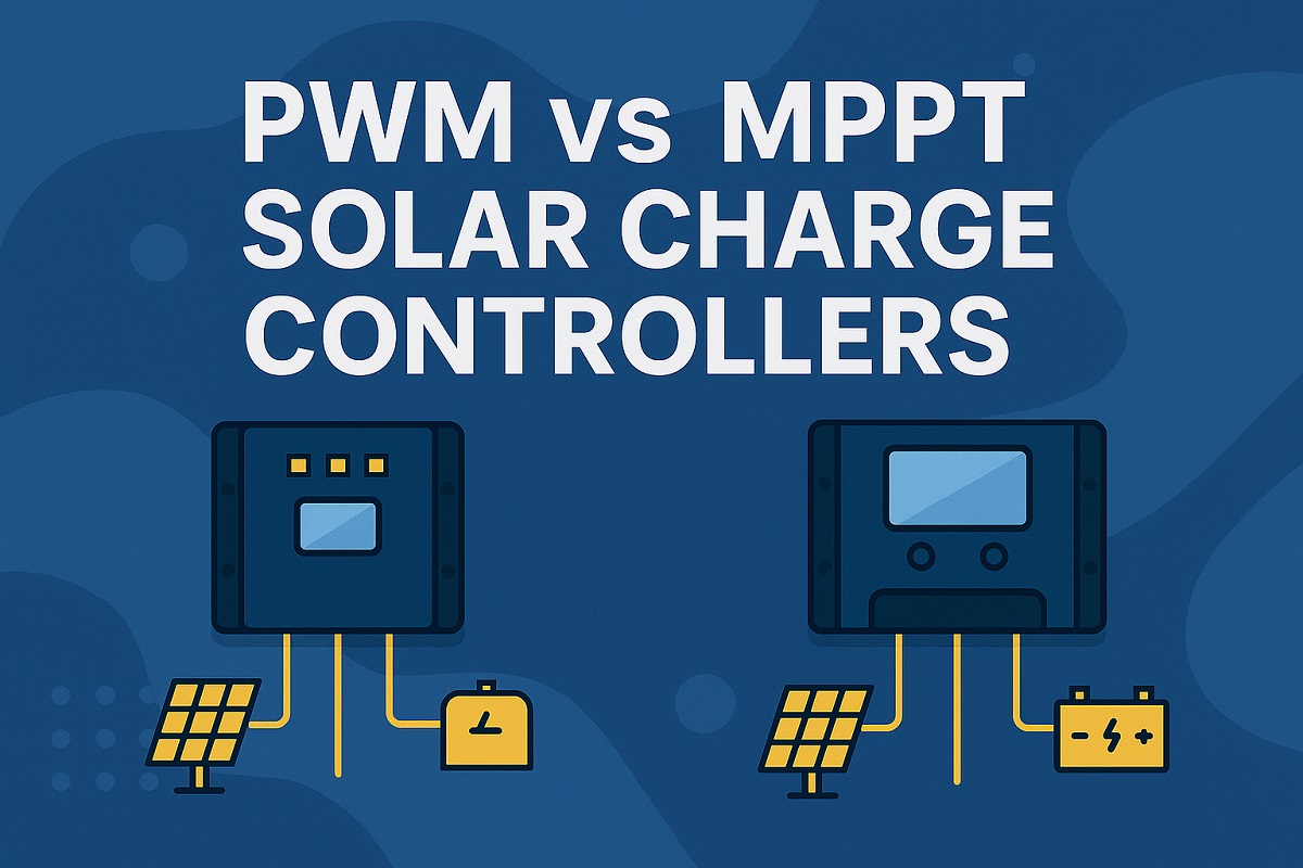 PWM vs MPPT Solar Charge Controllers: A Complete Comparison Guide
06 June 20254490
 What is a Great Choice for Digital Isolators to Build Isolation Barriers?
31 March 20225246
 What is Solid-state Battery
08 March 20216198
 0 Ohm Resistor Explained
10 December 202119923
 Various Reasons for the Failure, Explosion and Burning of Tantalum Capacitors
02 June 202211324
Analog Devices Inc.
In Stock: 70
Minimum: 1 Multiples: 1
Qty
Unit Price
Ext Price
1
$22.557888
$22.56
10
$21.281026
$212.81
100
$20.076440
$2,007.64
500
$18.940038
$9,470.02
1000
$17.867960
$17,867.96
Not the price you want? Send RFQ Now and we'll contact you ASAP.
Inquire for More Quantity
![ADF4118BRU-REEL7]() ADF4118BRU-REEL7
ADF4118BRU-REEL7Analog Devices Inc.
![AD9522-3BCPZ]() AD9522-3BCPZ
AD9522-3BCPZAnalog Devices Inc.
![AD9518-4ABCPZ]() AD9518-4ABCPZ
AD9518-4ABCPZAnalog Devices Inc.
![AD9517-3ABCPZ]() AD9517-3ABCPZ
AD9517-3ABCPZAnalog Devices Inc.
![AD9520-0BCPZ]() AD9520-0BCPZ
AD9520-0BCPZAnalog Devices Inc.
![AD9542BCPZ-REEL7]() AD9542BCPZ-REEL7
AD9542BCPZ-REEL7Analog Devices Inc.
![AD9574BCPZ]() AD9574BCPZ
AD9574BCPZAnalog Devices Inc.
![ADF4110BCPZ]() ADF4110BCPZ
ADF4110BCPZAnalog Devices Inc.
![ADF4113HVBRUZ]() ADF4113HVBRUZ
ADF4113HVBRUZAnalog Devices Inc.
![ADF4150HVBCPZ]() ADF4150HVBCPZ
ADF4150HVBCPZAnalog Devices Inc.


