
 Product
 Brand
Brand Articles
 Tools
Tools
MB10F Bridge Stack: Features, Pinout, and Datasheet [Video&FAQ]

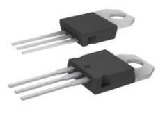
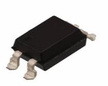
Single Phase Bridge Rectifier Surface Mount -55°C~150°C TJ 5μA @ 1000V 1.1V @ 800mA 4-Termination 1-Phase 4-SMD, Gull Wing Tape & Reel (TR)
Unit Price: $0.084529
Ext Price: $0.08


Single Phase Bridge Rectifier Surface Mount -55°C~150°C TJ 5μA @ 1000V 1.1V @ 800mA 4-Termination 1-Phase 4-SMD, Gull Wing Tape & Reel (TR)
MB10F is an ultra-thin SMD rectifier bridge stack, whose function is to convert alternating current into direct current, using the single-phase conductivity of the diode. This article mainly introduces features, pinout, datasheet and other detailed information about Diodes Incorporated MB10F.

Capacitive Dropper Circuit With MB10F
MB10F Description
MB10F is an ultra-thin SMD rectifier bridge stack, whose function is to convert alternating current into direct current, using the single-phase conductivity of the diode.
MB10F's foot pitch is 2.5mm, overall length is 4.7mm, height is 1.5mm, thickness is 0.6mm, and its body width is 4.0mm, the foot thickness is 0.25mm.
Designed for smaller and more energy-consuming application circuits, it is an ideal choice for the design of trendy electronic products.
The soldering pins are the same as those of MB6S, which can be directly replaced without changing the PCB board, which is of great help to the development of the production industry of miniaturized high-current products and is very suitable for portable applications that save circuit board space design.
MB10F Pinout
The following figure is the Pinout of MB10F.

Pinout
| Pin Number | Pin Name | Pin Description |
| 1 | Positive | Positive of Rectified Output |
| 2 | AC Input | AC Input |
| 3 | Negative | Negative of Rectified Output |
| 4 | AC Input | AC Input |
MB10F CAD Model
The followings are the Symbol, Footprint and 3D Model of MB10F.

Symbol

Footprint

3D Model
MB10F Features
● Glass Passivated Die Construction
● Miniature Package Saves Space On PC Boards
● Reliable Robust Construction
● Ideal For SMT Manufacturing
● Low Forward Voltage Drop
● Lead-Free Finish; RoHS Compliant
● Halogen And Antimony Free. “Green” Device
● Reverse Voltage - 100 To 1000 V
● Forward Current - 0.8 A
● High Surge Current Capability
● Designed For Surface-Mount Application
Specifications
- TypeParameter
- Factory Lead Time12 Weeks
- Mounting Type
The "Mounting Type" in electronic components refers to the method used to attach or connect a component to a circuit board or other substrate, such as through-hole, surface-mount, or panel mount.
Surface Mount - Package / Case
refers to the protective housing that encases an electronic component, providing mechanical support, electrical connections, and thermal management.
4-SMD, Gull Wing - Surface Mount
having leads that are designed to be soldered on the side of a circuit board that the body of the component is mounted on.
YES - Diode Element Material
The parameter "Diode Element Material" refers to the specific semiconductor material used in the construction of a diode. This material determines the electrical characteristics and performance of the diode, including its forward voltage drop, reverse breakdown voltage, and switching speed. Common diode element materials include silicon, germanium, and gallium arsenide, each offering different advantages for various applications. The choice of material impacts the diode's efficiency, thermal stability, and overall suitability for specific electronic circuits.
SILICON - Number of Elements4
- Operating Temperature
The operating temperature is the range of ambient temperature within which a power supply, or any other electrical equipment, operate in. This ranges from a minimum operating temperature, to a peak or maximum operating temperature, outside which, the power supply may fail.
-55°C~150°C TJ - Packaging
Semiconductor package is a carrier / shell used to contain and cover one or more semiconductor components or integrated circuits. The material of the shell can be metal, plastic, glass or ceramic.
Tape & Reel (TR) - Published2000
- JESD-609 Code
The "JESD-609 Code" in electronic components refers to a standardized marking code that indicates the lead-free solder composition and finish of electronic components for compliance with environmental regulations.
e3 - Pbfree Code
The "Pbfree Code" parameter in electronic components refers to the code or marking used to indicate that the component is lead-free. Lead (Pb) is a toxic substance that has been widely used in electronic components for many years, but due to environmental concerns, there has been a shift towards lead-free alternatives. The Pbfree Code helps manufacturers and users easily identify components that do not contain lead, ensuring compliance with regulations and promoting environmentally friendly practices. It is important to pay attention to the Pbfree Code when selecting electronic components to ensure they meet the necessary requirements for lead-free applications.
yes - Part Status
Parts can have many statuses as they progress through the configuration, analysis, review, and approval stages.
Active - Moisture Sensitivity Level (MSL)
Moisture Sensitivity Level (MSL) is a standardized rating that indicates the susceptibility of electronic components, particularly semiconductors, to moisture-induced damage during storage and the soldering process, defining the allowable exposure time to ambient conditions before they require special handling or baking to prevent failures
1 (Unlimited) - Number of Terminations4
- ECCN Code
An ECCN (Export Control Classification Number) is an alphanumeric code used by the U.S. Bureau of Industry and Security to identify and categorize electronic components and other dual-use items that may require an export license based on their technical characteristics and potential for military use.
EAR99 - Terminal Finish
Terminal Finish refers to the surface treatment applied to the terminals or leads of electronic components to enhance their performance and longevity. It can improve solderability, corrosion resistance, and overall reliability of the connection in electronic assemblies. Common finishes include nickel, gold, and tin, each possessing distinct properties suitable for various applications. The choice of terminal finish can significantly impact the durability and effectiveness of electronic devices.
Matte Tin (Sn) - Terminal Position
In electronic components, the term "Terminal Position" refers to the physical location of the connection points on the component where external electrical connections can be made. These connection points, known as terminals, are typically used to attach wires, leads, or other components to the main body of the electronic component. The terminal position is important for ensuring proper connectivity and functionality of the component within a circuit. It is often specified in technical datasheets or component specifications to help designers and engineers understand how to properly integrate the component into their circuit designs.
DUAL - Peak Reflow Temperature (Cel)
Peak Reflow Temperature (Cel) is a parameter that specifies the maximum temperature at which an electronic component can be exposed during the reflow soldering process. Reflow soldering is a common method used to attach electronic components to a circuit board. The Peak Reflow Temperature is crucial because it ensures that the component is not damaged or degraded during the soldering process. Exceeding the specified Peak Reflow Temperature can lead to issues such as component failure, reduced performance, or even permanent damage to the component. It is important for manufacturers and assemblers to adhere to the recommended Peak Reflow Temperature to ensure the reliability and functionality of the electronic components.
NOT SPECIFIED - Reach Compliance Code
Reach Compliance Code refers to a designation indicating that electronic components meet the requirements set by the Registration, Evaluation, Authorization, and Restriction of Chemicals (REACH) regulation in the European Union. It signifies that the manufacturer has assessed and managed the chemical substances within the components to ensure safety and environmental protection. This code is vital for compliance with regulations aimed at minimizing risks associated with hazardous substances in electronic products.
not_compliant - Time@Peak Reflow Temperature-Max (s)
Time@Peak Reflow Temperature-Max (s) refers to the maximum duration that an electronic component can be exposed to the peak reflow temperature during the soldering process, which is crucial for ensuring reliable solder joint formation without damaging the component.
NOT SPECIFIED - JESD-30 Code
JESD-30 Code refers to a standardized descriptive designation system established by JEDEC for semiconductor-device packages. This system provides a systematic method for generating designators that convey essential information about the package's physical characteristics, such as size and shape, which aids in component identification and selection. By using JESD-30 codes, manufacturers and engineers can ensure consistency and clarity in the specification of semiconductor packages across various applications and industries.
R-PDSO-G4 - Configuration
The parameter "Configuration" in electronic components refers to the specific arrangement or setup of the components within a circuit or system. It encompasses how individual elements are interconnected and their physical layout. Configuration can affect the functionality, performance, and efficiency of the electronic system, and may influence factors such as signal flow, impedance, and power distribution. Understanding the configuration is essential for design, troubleshooting, and optimizing electronic devices.
BRIDGE, 4 ELEMENTS - Diode Type
In electronic components, the parameter "Diode Type" refers to the specific type or configuration of a diode, which is a semiconductor device that allows current to flow in one direction only. There are various types of diodes, each designed for specific applications and functions. Common diode types include rectifier diodes, zener diodes, light-emitting diodes (LEDs), and Schottky diodes, among others. The diode type determines the diode's characteristics, such as forward voltage drop, reverse breakdown voltage, and maximum current rating, making it crucial for selecting the right diode for a particular circuit or application. Understanding the diode type is essential for ensuring proper functionality and performance in electronic circuits.
Single Phase - Current - Reverse Leakage @ Vr
Current - Reverse Leakage @ Vr is a parameter that describes the amount of current that flows in the reverse direction through a diode or other semiconductor component when a reverse voltage (Vr) is applied across it. This leakage current is typically very small, but it is important to consider in electronic circuits as it can affect the overall performance and reliability of the component. The reverse leakage current is influenced by factors such as the material properties of the semiconductor, temperature, and the magnitude of the reverse voltage applied. Manufacturers provide this parameter in datasheets to help engineers and designers understand the behavior of the component in reverse bias conditions.
5μA @ 1000V - Voltage - Forward (Vf) (Max) @ If
The parameter "Voltage - Forward (Vf) (Max) @ If" refers to the maximum voltage drop across a diode when it is forward-biased and conducting a specified forward current (If). It indicates the maximum potential difference the diode can withstand while allowing current to flow in the forward direction without breaking down. This value is crucial for designing circuits as it helps determine how much voltage will be lost across the diode during operation. Higher Vf values can lead to reduced efficiency in power applications, making this parameter essential for optimizing circuit performance.
1.1V @ 800mA - Output Current-Max
Output Current-Max is a parameter in electronic components that specifies the maximum amount of current that can be safely drawn from the output of the component without causing damage. It is an important specification to consider when designing circuits to ensure that the component can handle the required current without overheating or failing. Exceeding the maximum output current can lead to performance issues, component damage, or even complete failure of the circuit. It is crucial to adhere to the specified maximum output current to ensure the reliable operation of the electronic component and the overall circuit.
0.8A - Current - Average Rectified (Io)
The parameter "Current - Average Rectified (Io)" in electronic components refers to the average value of the rectified current flowing through the component. This parameter is important in determining the average power dissipation and thermal considerations of the component. It is typically specified in datasheets for diodes, rectifiers, and other components that handle alternating current (AC) and convert it to direct current (DC). Understanding the average rectified current helps in selecting the appropriate component for a given application to ensure reliable operation and prevent overheating.
800mA - Number of Phases1
- Non-rep Pk Forward Current-Max
Non-rep Pk Forward Current-Max refers to the maximum forward current that a semiconductor device, such as a diode or LED, can handle in a pulsed or non-repetitive manner without being damaged. This parameter is essential for designers to ensure that the component operates reliably under specific conditions, particularly during transient events like switching or fault conditions. Exceeding this limit can lead to overheating or failure of the device.
30A - Voltage - Peak Reverse (Max)
Voltage - Peak Reverse (Max) refers to the maximum voltage that a semiconductor device, typically a diode, can withstand in the reverse-bias direction without undergoing breakdown. It is crucial for ensuring reliable operation in circuits where the direction of the voltage may change. Exceeding this parameter can result in permanent damage to the component, leading to failure in its intended function. This specification is particularly important in applications involving rectification or signal modulation.
1kV - Breakdown Voltage-Min
Breakdown Voltage-Min, also known as minimum breakdown voltage, is a crucial parameter in electronic components, especially in devices like diodes, transistors, and capacitors. It refers to the minimum voltage at which the component experiences a breakdown and allows a significant current to flow through it. This breakdown voltage is a critical threshold beyond which the component may get damaged or exhibit unexpected behavior. Manufacturers specify this parameter to ensure that the component operates within safe limits and to help designers select the appropriate components for their circuit requirements. It is essential to consider the Breakdown Voltage-Min when designing circuits to prevent overloading or damaging the components.
1000V - RoHS Status
RoHS means “Restriction of Certain Hazardous Substances” in the “Hazardous Substances Directive” in electrical and electronic equipment.
ROHS3 Compliant
How to use MB10F Bridge Rectifier
The MB10F is a pretty straightforward device to operate. As the name implies, the IC is a complete bridge rectifier, which is nothing more than a four-diode design as illustrated below.

The simulated circuit below depicts how a bridge rectifier acts when an AC voltage is applied to the AC side of the rectifier, and a smoothing capacitor is used to rectify the pulsed DC signal to a smoother out DC signal on the DC side. The formula can be used to compute the IC's output DC voltage.
DC Out = (√2×VRMS) – 1.1 Volts
Where VRMS is the input RMS voltage and -1.1V is the voltage drop that occurs during rectification across each diode line. Though we will not receive that in our simulation because all devices in the simulation are ideal devices.
MB10F Circuit Diagram
The following figure is the Circuit Diagram of MB10F.

Circuit Diagram
MB10F Layout

MB10F Alternative
MB10F Applications
MB10F Package
The following figure is the Package of MB10F.

Package
MB10F Manufacturer
Diodes Incorporated is devoted to being the leading provider for large-volume and high-growing markets. With cutting-edge products of package technology, analog, discrete and mixed-signal products, Diodes Incorporated is capable to provide high-quality semiconductor products to meet the customers’ needs from walks of communications, computing, consumer electronics, automotive and industrial markets. Their product lines cover a wide range of application solutions together with 25 operations around the world which serve with the examination, engineering, manufacturing and customer service.
Trend Analysis
Datasheet PDF
- Environmental Information :
- Datasheets :
1.What is MB10F circuit?
MB10F Bridge Rectifier MB10f is a surface Mount Glass passivated bridge rectifier with a Maximum Peak reverse voltage of 1000 volts and an average output current of 0.8 Ampere. Features of MB10F: Plastic material has U/L flammability classification 94V-O. High surge overload rating 35A peak. Saves space on the printed circuit.
2.Is the rectifier bridge MB10F the same as ABS10?
If there is no circuit designed, it can be used. If the circuit board is determined, it cannot be universal, because the pin positions are different. In addition, ABS10 defaults to 1 ampere current 1000V withstand voltage, MB10F is 0.8 amperes current 1000V withstand voltage.
3.Are the parameters of MB10F and MB10S consistent?
The body height of the MB10S bridge stack is 2.5mm, the MB10F 10S has a thickness of 1.1mm, and the MB10F has a thickness of 0.6mm, so it is concluded that the parameters of the two rectifier bridges are the same, but the MB10F is thinner and smaller than the MB10S. Products with high requirements on the volume of the rectifier bridge.
4. What is the name of the ultra-thin MB10F?
SMD rectifier bridge stack.
5. What is the foot pitch of MB10F?
2.5mm.
6. What type of products is MB10F ideal for?
Electronic.
7. The soldering pins are the same as what?
MB6S.
 TYN612 Thyristor: Application Circuit, Datasheet, Pinout
04 November 202117249
 What is the difference between them: 2N3904 vs. BC547?
10 November 202131536
 IRF640 Power MOSFET: Datasheet, Pinout, and Circuits
28 August 202112011
 IS181 Optocoupler: Datasheet, Pinout and Applications
29 July 20212768
 SFH620A Optocoupler: Datasheet, Pinout, Circuit
09 March 20222222
 AT89C51CC03: Enhanced 8-bit MCU with CAN Controller and Flash Memory
28 February 2024329
 STM8S207C6T6 Microcontroller: Pinout, Datasheet and Features
14 July 20213763
![BTA12 Triacs: Features, Pinout, and Datasheet [Video&FAQ]](https://res.utmel.com/Images/Article/0e2fa5b3-b023-4f7c-8a16-fb7d7e7972ef.png) BTA12 Triacs: Features, Pinout, and Datasheet [Video&FAQ]
BTA12 Triacs: Features, Pinout, and Datasheet [Video&FAQ]04 December 202115521
 CCTC Authorized Distributor | UTMEL Electronics
22 February 20257604
 Volkswagen Overhauls Semiconductor Sourcing Strategy Amid Supply Challenges
01 September 20234549
 How to Pick the Perfect Boost Converter for Your Needs
07 June 20251289
 Top Picks for Circuit Breakers This Year
10 July 20256632
 High-Frequency Silicon Carbide MOSFETs using Resonant Gate Driver Circuits
13 March 20241879
 An Overview of Development Board
18 December 202515322
 A New Way of Thinking About the "Trolley Problem" of Artificial Intelligence
27 May 20221727
 What is an Inverting Amplifier?
25 April 202511819
Diodes Incorporated
In Stock: 5000
Minimum: 1 Multiples: 1
Qty
Unit Price
Ext Price
1
$0.084529
$0.08
10
$0.079744
$0.80
100
$0.075231
$7.52
500
$0.070972
$35.49
1000
$0.066955
$66.96
Not the price you want? Send RFQ Now and we'll contact you ASAP.
Inquire for More Quantity


