
UA741 Operational Amplifier Series: Technical Design Guide & Datasheet Analysis

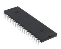
1 Channels 25mA per Channel 10nA 70 dB Instrumentational OP Amps 0.2μA 20V 10V~44V ±5V~22V UA741 8 Pins 8-DIP (0.300, 7.62mm)


1 Channels 25mA per Channel 10nA 70 dB Instrumentational OP Amps 0.2μA 20V 10V~44V ±5V~22V UA741 8 Pins 8-DIP (0.300, 7.62mm)
Deep dive into STMicroelectronics UA741 Op-Amp: datasheet specs, pinout strategy, frequency compensation, and PCB layout guide for analog engineers.
Key Takeaway
Positioning: The UA741 by STMicroelectronics is the industry-standard "workhorse" monolithic operational amplifier. While legacy in architecture, it remains a primary choice for general-purpose analog signal conditioning, educational prototyping, and robust control loops due to its inherent stability and latch-up immunity.
Key Spec Highlight: Features short-circuit protection and internal frequency compensation, eliminating the need for external stabilization components in most gain configurations.
Supply Chain Status: Active. Widely available from STMicroelectronics and second-source manufacturers, ensuring long-term support for legacy and new designs.

UA741 product photo
1. Technical Architecture and Core Advantages
The UA741 is a high-performance monolithic operational amplifier built on a single silicon chip. Unlike early op-amps that required complex external compensation networks, the UA741 integrates these protections, making it significantly easier to implement in variable voltage designs.
1.1 Processing & Control (The "Brain")
The core architecture of the UA741 is defined by its robust differential input stage and high-gain voltage amplification topology.
- Latch-Up Immunity: The design specifically prevents latch-up, a common failure mode in earlier amplifier generations where the output locks to a supply rail.
- Internal Compensation: The chip includes an internal capacitor (typically 30pF in this class of architecture) that sets the dominant pole, ensuring stability for unity-gain configurations. This limits the Gain Bandwidth Product (GBP) to 1 MHz but guarantees "plug-and-play" stability.
1.2 Peripherals & Interfaces (The "Limbs")
The UA741 offers a standard 8-pin interface optimized for analog flexibility:
Offset Nulling: Pins 1 and 5 allow designers to nullify input offset voltage using an external potentiometer, critical for precision DC applications.
Input Protection: The wide common-mode and differential voltage ranges allow the inputs to handle significant signal variance without damage.
Output Stage: The Class AB output stage provides short-circuit protection, safeguarding the device against accidental shorts to ground or supply rails.

UA741 functional block diagram internal architecture
2. Naming / Variant Map and Selection Guide
2.1 Part Number Decoding
The UA741 part numbering system follows a logical suffix structure indicating temperature grade and package type.
Prefix (UA741): Base part number for the Operational Amplifier series.
First Suffix (Temp Grade): * C = Commercial Temperature Range (0°C to +70°C).
I = Industrial Temperature Range (-40°C to +105°C).
Second Suffix (Package):
N = DIP-8 (Dual In-line Package, Through-hole).
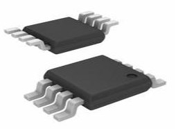
D = SO-8 (Small Outline Package, Surface Mount).
2.2 Core Variant Comparison
| Variant | Key Differences | Flash/RAM | Package | Target Use |
|---|---|---|---|---|
| UA741CN | Commercial Temp (0 to 70°C) | N/A | DIP-8 | Prototyping, Education, Consumer Electronics |
| UA741CD | Commercial Temp (0 to 70°C) | N/A | SO-8 | Compact Consumer PCBs |
| UA741IN | Industrial Temp (-40 to 105°C) | N/A | DIP-8 | Industrial Control, Legacy Repair |
| UA741ID | Industrial Temp (-40 to 105°C) | N/A | SO-8 | Robust Industrial Hardware |
3. Key Specifications Explained
Engineer's Note: Values below are typical. Always consult the specific datasheet (UA741-1852616) for max/min limits.
3.1 Power & Operating Conditions
The UA741 is a high-voltage bipolar device, not a modern low-voltage CMOS op-amp. - Supply Voltage (Vcc): Rated regarding an Absolute Maximum of ±22V. Standard operation usually targets ±15V.
Input Voltage Range: typically ±15V (when Vcc is ±15V).
Power Implication: This device is not optimized for low-voltage battery applications (e.g., 3.3V IoT nodes). It thrives in dual-supply environments found in audio mixers, industrial controllers, and bench equipment.
3.2 Performance & Efficiency
Slew Rate: 0.5 V/µs. This is the speed limit of the output voltage change.
Impact: It limits the full-power bandwidth. For high-frequency signals, the output will distort into a triangle wave if the slew rate is exceeded.
Gain Bandwidth Product (GBP): 1 MHz.
Short Circuit Protection: indefinite duration (for supply voltages < 15V).
4. Design Notes and Common Integration Issues
4.1 PCB Layout Guidelines
Proper layout ensures the UA741 performs without oscillation or excessive noise. - Power Rails: Place 0.1µF ceramic decoupling capacitors as close as possible to the VCC+ (Pin 7) and VCC- (Pin 4) pins to suppress high-frequency noise. - Grounding: Separate analog and digital grounds. The UA741 does not have a dedicated GND pin; it references the midpoint of the split supplies. Ensure the load return path is low impedance. - Trace Routing: Keep the inverting input (Pin 2) and non-inverting input (Pin 3) traces as short as possible to minimize stray capacitance, which can degrade phase margin.

UA741 pinout diagram and footprint
4.2 Debugging Common Faults (Pain Points)
The following issues are common integration hurdles derived from engineering field data.
Problem 1: Signal Distortion at High Frequencies- Symptom: Output waveform looks triangular or clipped when frequency increases, even if gain is low. - Root Cause: Low Slew Rate (0.5 V/µs). The op-amp cannot change its output voltage fast enough to track the input. - Fix: Calculate the required slew rate ($SR \approx 2 \pi f V_{peak}$). If the requirement exceeds 0.5 V/µs, migrate to a TL071 or NE5534.
Problem 2: Output Clipping Below Supply Rails- Symptom: Using a ±15V supply, the output clips at ±13V. - Root Cause: Limited Output Swing. The UA741 is not a Rail-to-Rail device. Bipolar output transistors require voltage headroom (saturation voltage).
Fix: Ensure supply rails are at least 2-3V higher than the maximum required output peak. For rail-to-rail precision, choose a CMOS alternative.
5. Typical Applications
📺 Video Recommendation: UA741 Guide
5.1 System Integration Analysis
Application: Voltage Follower (Buffer)The UA741 is frequently used as a unity-gain buffer to isolate high-impedance sensors from low-impedance loads.
- Why UA741? Its high input impedance prevents loading the sensor, while its low output impedance can drive subsequent stages. The internal compensation ensures the buffer remains stable despite the 100% negative feedback loop (unity gain is the most prone to oscillation in uncompensated amps).
Configuration: Connect Output (Pin 6) directly to Inverting Input (Pin 2). Signal enters Non-Inverting Input (Pin 3).
6. Competitors and Alternatives
The UA741 competes in the "General Purpose Bipolar Op-Amp" category.
- Vs. Texas Instruments LM741: Functionally identical. The LM741 is the direct equivalent with the same pinout and similar specs. Selection often depends on stock availability and price per reel.
- Vs. Analog Devices AD741: Often offers tighter specs on offset voltage drift in precision grades, but generally higher cost.
- Migration Path:
Need Higher Speed? Upgrade to TL081 (JFET input, faster slew rate).
Need Rail-to-Rail? Upgrade to TLV2371 or similar CMOS op-amps.
Drop-in Replacement: Most "741" designated chips (LM741, MC1741, uA741) are pin-compatible.
7. FAQ
Q: What is the absolute maximum supply voltage for the UA741?
The absolute maximum supply voltage is ±22V, though ±15V is the standard operating condition.
Q: Does the UA741 require external frequency compensation?
No, the UA741 features internal frequency compensation, making it stable at unity gain without external capacitors.
Q: Can I use the UA741 with a single power supply?
Yes, but it requires a virtual ground reference (typically Vcc/2) at the inputs to bias the signal within the linear operating range.
Q: What represents the main difference between UA741CN and UA741IN?
The "C" suffix denotes Commercial temperature range (0°C to 70°C), while the "I" denotes Industrial temperature range (-40°C to 105°C).
Q: How do I adjust the input offset voltage on a UA741?
Connect a 10kΩ potentiometer between Pin 1 and Pin 5, with the wiper connected to the negative supply rail (VEE).
8. Resources and Downloads
Datasheet: UA741-1852616 PDF Download
Dev Tools: Breadboard, Analog Discovery Kit (for characterization).
Specifications
Datasheet PDF
- Datasheets :
 AD8233ACBZ-R7 Heart Rate Monitor: Low Noise, 20WLCSP Monitor and AD8233 Datasheet
21 January 20221674
 ATMEGA1284P Microcontroller: Pinout, Datasheet, ATMEGA1284 vs. ATMEGA1284P
18 November 20214370
![ICL7660S Voltage Regulators DC Switching Regulators[Video]:Datasheet, Pinout, and Applications.](https://res.utmel.com/Images/Article/91a532a5-68a0-4d45-acb6-10f0b31c4052.png) ICL7660S Voltage Regulators DC Switching Regulators[Video]:Datasheet, Pinout, and Applications.
ICL7660S Voltage Regulators DC Switching Regulators[Video]:Datasheet, Pinout, and Applications.01 April 20222133
 C1815 NPN Transistor: Pinout, Equivalents, and Uses
11 August 202141890
 7815 Voltage Regulator: 15V Voltage Regulator, 7815 Pinout, Datasheet
14 January 202227136
 AD9856ASTZ IC Upconverter: Specification, Pinout, Datasheet
14 August 2024365
 LR43 VS LR44 VS LR41: Can I Use LR43 or LR41 Instead of LR44?
04 March 202278231
 IL511 Digital Isolators: Datasheet, Pinout and Applications
28 August 2021395
 Top 10 IC Design Companies in China
13 January 20228369
 Tunnel Diode: Definition, Features and Tunneling Process
25 August 20209886
 What is Solenoid Valve? How to Choose a Solenoid Valve?
06 January 20223069
 The Understanding to Autonomous Driving Sensor
10 November 20211147
 The Introduction to PCB Inspection Knowledge and Methods
22 December 20212881
 What is a Schmitt Trigger?
09 December 20216790
 Application Specific Trade-offs for WBG SIC, GaN and High End SI Power Switch Technologies
22 November 20221462
 Discovering Optimal Materials for Wide Bandgap Semiconductors
20 January 20242053
STMicroelectronics
In Stock: 250
United States
China
Canada
Japan
Russia
Germany
United Kingdom
Singapore
Italy
Hong Kong(China)
Taiwan(China)
France
Korea
Mexico
Netherlands
Malaysia
Austria
Spain
Switzerland
Poland
Thailand
Vietnam
India
United Arab Emirates
Afghanistan
Åland Islands
Albania
Algeria
American Samoa
Andorra
Angola
Anguilla
Antigua & Barbuda
Argentina
Armenia
Aruba
Australia
Azerbaijan
Bahamas
Bahrain
Bangladesh
Barbados
Belarus
Belgium
Belize
Benin
Bermuda
Bhutan
Bolivia
Bonaire, Sint Eustatius and Saba
Bosnia & Herzegovina
Botswana
Brazil
British Indian Ocean Territory
British Virgin Islands
Brunei
Bulgaria
Burkina Faso
Burundi
Cabo Verde
Cambodia
Cameroon
Cayman Islands
Central African Republic
Chad
Chile
Christmas Island
Cocos (Keeling) Islands
Colombia
Comoros
Congo
Congo (DRC)
Cook Islands
Costa Rica
Côte d’Ivoire
Croatia
Cuba
Curaçao
Cyprus
Czechia
Denmark
Djibouti
Dominica
Dominican Republic
Ecuador
Egypt
El Salvador
Equatorial Guinea
Eritrea
Estonia
Eswatini
Ethiopia
Falkland Islands
Faroe Islands
Fiji
Finland
French Guiana
French Polynesia
Gabon
Gambia
Georgia
Ghana
Gibraltar
Greece
Greenland
Grenada
Guadeloupe
Guam
Guatemala
Guernsey
Guinea
Guinea-Bissau
Guyana
Haiti
Honduras
Hungary
Iceland
Indonesia
Iran
Iraq
Ireland
Isle of Man
Israel
Jamaica
Jersey
Jordan
Kazakhstan
Kenya
Kiribati
Kosovo
Kuwait
Kyrgyzstan
Laos
Latvia
Lebanon
Lesotho
Liberia
Libya
Liechtenstein
Lithuania
Luxembourg
Macao(China)
Madagascar
Malawi
Maldives
Mali
Malta
Marshall Islands
Martinique
Mauritania
Mauritius
Mayotte
Micronesia
Moldova
Monaco
Mongolia
Montenegro
Montserrat
Morocco
Mozambique
Myanmar
Namibia
Nauru
Nepal
New Caledonia
New Zealand
Nicaragua
Niger
Nigeria
Niue
Norfolk Island
North Korea
North Macedonia
Northern Mariana Islands
Norway
Oman
Pakistan
Palau
Palestinian Authority
Panama
Papua New Guinea
Paraguay
Peru
Philippines
Pitcairn Islands
Portugal
Puerto Rico
Qatar
Réunion
Romania
Rwanda
Samoa
San Marino
São Tomé & Príncipe
Saudi Arabia
Senegal
Serbia
Seychelles
Sierra Leone
Sint Maarten
Slovakia
Slovenia
Solomon Islands
Somalia
South Africa
South Sudan
Sri Lanka
St Helena, Ascension, Tristan da Cunha
St. Barthélemy
St. Kitts & Nevis
St. Lucia
St. Martin
St. Pierre & Miquelon
St. Vincent & Grenadines
Sudan
Suriname
Svalbard & Jan Mayen
Sweden
Syria
Tajikistan
Tanzania
Timor-Leste
Togo
Tokelau
Tonga
Trinidad & Tobago
Tunisia
Turkey
Turkmenistan
Turks & Caicos Islands
Tuvalu
U.S. Outlying Islands
U.S. Virgin Islands
Uganda
Ukraine
Uruguay
Uzbekistan
Vanuatu
Vatican City
Venezuela
Wallis & Futuna
Yemen
Zambia
Zimbabwe


