Product
 Brand
Brand Articles
 Tools
Tools
ADXL345 3-Axis Digital Accelerometer: Technical Design Guide and Datasheet Analysis


ACCEL 2-16G I2C/SPI 14LGA
The ADXL345 is an ultralow power 3-axis accelerometer offering 13-bit resolution and ±16 g range. This guide covers pinout, SPI/I2C integration, and PCB layout for reliable motion sensing circuits.
Product Introduction
Engineer's Takeaway
For embedded architects, the ADXL345 represents a balance between high-resolution sensing and extreme power efficiency. Unlike basic analog accelerometers, its integrated digital logic handles event detection (taps, inactivity), offloading the host MCU.
- Positioning: Designed for mobile device applications where battery life is critical but precise motion context (portrait/landscape, step counting) is required.
- Key Spec Highlight: Ultralow power consumption, drawing as little as 23 µA in measurement mode and significantly less in standby.
- Supply Chain Status: Active but High Risk. While the part is widely produced, the market is flooded with counterfeit clones (often remarked generic parts). Procurement from authorized distributors (Mouser/DigiKey) is mandatory to ensure datasheet compliance.

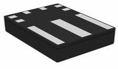
ADXL345 LGA-14 package overview
1. Technical Architecture and Core Advantages
The ADXL345 is a complete 3-axis acceleration measurement system based on polysilicon surface-micromachined sensor and signal conditioning circuitry. It measures static acceleration of gravity in tilt-sensing applications, as well as dynamic acceleration resulting from motion or shock.
1.1 Processing & Control
The core of the ADXL345 features a proprietary memory management system that differentiates it from simpler sensors:
Integrated FIFO (First In, First Out): A 32-level FIFO buffer stores data to minimize host processor intervention. This allows the host MCU to sleep while the ADXL345 collects samples, only waking up when the buffer is full—a critical feature for IoT battery optimization.
Motion Detection Engine: Internal logic blocks handle complex event detection hardware-side:
Single/Double Tap: Configurable threshold and duration.
Free-Fall: Detects if the device is falling (0g on all axes).
Inactivity: Switches the system to sleep mode if no motion is detected for a set time.
1.2 Peripherals & Interfaces
The device offers flexible connectivity options to suit various microcontroller constraints:
Dual Serial Interface: Supports both I2C and SPI (3-wire or 4-wire) digital interfaces.
Interrupt Pins (INT1, INT2): Two programmable interrupt pins can be mapped to specific events (e.g., Data Ready, Free Fall, Watermark), allowing for sophisticated wake-up schemes.
Resolution Control: The user can select ranges (±2 g, ±4 g, ±8 g, ±16 g). In full-resolution mode, the device maintains a scale factor of 3.9 mg/LSB, ensuring that resolution increases as the range increases (up to 13-bit).
2. Naming / Variant Map and Selection Guide
2.1 Part Number Decoding
The ADXL345 follows a specific naming convention defined by Analog Devices. Understanding the suffixes is key to ordering the correct package and reel size.
- ADXL: Accelerometer Product Line
- 345: Part ID (Digital, 3-Axis)
- B: Revision or Temperature Grade (Industrial)
- CC: Package Designator (LGA - Land Grid Array)
- Z: RoHS Compliant (Lead-free)
- -RL / -RL7: Shipping format (Tape and Reel sizes)
2.2 Core Variant Comparison
Since the ADXL345 is a specific singular part number, variants differ mainly by shipping packaging.
| Variant | Package Type | Shipping Format | Target Use |
|---|---|---|---|
| ADXL345BCCZ | LGA-14 (3mm × 5mm × 1mm) | Tray / Cut Tape | Prototyping / Low Volume |
| ADXL345BCCZ-RL | LGA-14 | 13-inch Tape & Reel | Automated Assembly (High Vol) |
| ADXL345BCCZ-RL7 | LGA-14 | 7-inch Tape & Reel | Medium Volume Production |
3. Key Specifications Explained
Engineer's Note: Values below are typical at $V_S = 2.5 V$. Always consult the specific datasheet for max/min limits across the temperature range of -40°C to +85°C.
3.1 Power & Operating Conditions
The ADXL345 is purpose-built for battery-operated systems. - Supply Voltage (Vs): 2.0 V to 3.6 V. Ideally suited for 3.3V logic or unregulated Li-Po usage (via LDO).
I/O Voltage (Vdd_io): Separate supply pin allows direct interfacing with 1.8V logic while Vs remains higher.
Current Consumption:
Measurement Mode: 23 µA to 140 µA (depends on output data rate).
Standby Mode: typically 0.1 µA.
Implication: At 23 µA, an ADXL345 can run for years on a standard CR2032 coin cell, provided the host MCU sleeps effectively.
3.2 Performance & Efficiency
Resolution: Up to 13-bit (at ±16 g). This provides high precision (approx 3.9 mg/LSB), sufficient to detect tilt changes of less than 1 degree.
Output Data Rate (ODR): Selectable from 0.1 Hz to 3200 Hz. Lower rates conserve power significantly.
Zero-g Offset: Tightly trimmed at the factory, though software calibration is recommended for high-precision inclinometer applications.

4. Design Notes and Common Integration Issues
Integrating MEMS sensors into a PCB requires careful attention to mechanical stress and electrical noise.
4.1 PCB Layout Guidelines
Proper layout ensures data integrity and reduces noise in the accelerometer readings.
- Power Rails: Place a 0.1 µF ceramic capacitor and a 10 µF tantalum/ceramic capacitor as close as possible to the $V_S$ and $V_{DD I/O}$ pins to reject power supply noise.
- Grounding: Connect the GND pins to a solid ground plane. Avoid routing high-speed switching signals under the sensor which could capacitively couple noise into the MEMS structure.
- Mechanical Stress: Do not place the LGA package near screw holes or PCB edges. Board flexing can introduce mechanical offset errors (stress-induced bias).
Solder Mask: Use Non-Solder Mask Defined (NSMD) pads for the LGA footprint to reduce stress transfer to the package.
4.2 Debugging Common Faults (Pain Points)
Problem 1: Inconsistent or "Random" Data Readings- Symptom: The device ID reads correctly, but X/Y/Z data seems like garbage or static. - Root Cause: Counterfeit ICs. The market is flooded with cloned sensors that report the correct Device ID but fail to operate the MEMS core correctly. - Fix: Purchase exclusively from authorized distributors (Mouser, DigiKey, Arrow). Do not trust "generic module" vendors on marketplaces for production designs.
Problem 2: Communication Failure (No ACK on I2C)- Symptom: MCU cannot talk to the chip.
- Root Cause: Incorrect CS pin state. For I2C mode, the CS pin must be tied high ($V_{DD I/O}$). If left floating or low, the chip may enter SPI mode.
- Fix: Ensure CS is hard-wired high for I2C and verify pull-up resistors on SDA/SCL.
Problem 3: LGA Soldering Difficulties- Symptom: Cold solder joints or bridged pins on the 14-pin LGA package. - Root Cause: The LGA package has pads underneath the body, making hand-soldering nearly impossible without hot air, and difficult to inspect. - Fix: For prototyping, use a breakdown board (like the Adafruit or SparkFun modules). For production, follow the IPC reflow profile strictly and consider X-ray inspection for the first batch.
5. Typical Applications
5.1 System Integration Analysis: Battery-Powered Asset Tracker
In an asset tracking application, the ADXL345 serves as the system's "watchdog." - Challenge: The GPS and LTE modem consume too much power to stay on. - Solution: The ADXL345 is configured in Activity Detection mode with a low threshold (e.g., 0.5 g). The system stays in deep sleep (uA range).
Operation: When the asset moves, the ADXL345 triggers an interrupt via pin INT1. The MCU wakes up, powers the GPS, fixes location, transmits, and returns to sleep.
Benefit: This architecture extends battery life from days to months by ensuring high-power components only run when physical movement occurs.

ADXL345 typical application circuit schematic
6. Competitors and Alternatives
The ADXL345 is a legacy industry standard, but modern alternatives exist.
- Vs. STMicroelectronics LIS3DH: The LIS3DH is often cheaper and pin-compatible (mostly) with similar low-power characteristics. It is a strong competitor for cost-sensitive high-volume designs.
- Vs. Bosch BMA250: Known for extremely low offset and high stability, often preferred in automotive or precision industrial contexts.
- Vs. MPU-6050: If your application requires rotation sensing (Gyroscopes), the MPU-6050 (6-axis IMU) is the upgrade path, though it consumes significantly more power than the standalone ADXL345 accelerator.
7. FAQ
Q: What is the absolute maximum voltage for ADXL345?
The absolute maximum rating for $V_S$ is 3.9 V. Exceeding this, even momentarily, can cause permanent damage. A regulated 2.5 V or 3.3 V supply is recommended.
Q: Does ADXL345 support 5V logic?
No, the ADXL345 is not 5V tolerant. Connecting 5V I2C/SPI lines directly will destroy the digital I/O. You must use a logic level shifter if interfacing with a 5V MCU (like an Arduino Uno).
Q: What represents the main difference between ADXL345 and ADXL343?
The ADXL343 is largely a cost-down version of the ADXL345. While they share similar pinouts and registers, the ADXL345 generally offers tighter specifications on temperature stability and offset performance.
Q: How do I select between SPI and I2C modes?
The communication mode is determined by the state of the Chip Select (CS) pin. Tying CS high enables I2C; driving CS low enables SPI.
8. Resources and Downloads
Datasheet: ADXL345 Datasheet (Analog Devices)
Dev Tools: Evaluation boards (EVAL-ADXL345Z) and verified breakout modules (SparkFun/Adafruit) are widely available.
Specifications
- TypeParameter
- Lifecycle Status
Lifecycle Status refers to the current stage of an electronic component in its product life cycle, indicating whether it is active, obsolete, or transitioning between these states. An active status means the component is in production and available for purchase. An obsolete status indicates that the component is no longer being manufactured or supported, and manufacturers typically provide a limited time frame for support. Understanding the lifecycle status is crucial for design engineers to ensure continuity and reliability in their projects.
PRODUCTION (Last Updated: 3 months ago) - Factory Lead Time8 Weeks
- Contact Plating
Contact plating (finish) provides corrosion protection for base metals and optimizes the mechanical and electrical properties of the contact interfaces.
Tin - Mounting Type
The "Mounting Type" in electronic components refers to the method used to attach or connect a component to a circuit board or other substrate, such as through-hole, surface-mount, or panel mount.
Surface Mount - Package / Case
refers to the protective housing that encases an electronic component, providing mechanical support, electrical connections, and thermal management.
14-VFLGA - Surface Mount
having leads that are designed to be soldered on the side of a circuit board that the body of the component is mounted on.
YES - Number of Pins14
- Operating Temperature
The operating temperature is the range of ambient temperature within which a power supply, or any other electrical equipment, operate in. This ranges from a minimum operating temperature, to a peak or maximum operating temperature, outside which, the power supply may fail.
-55°C~105°C TA - Packaging
Semiconductor package is a carrier / shell used to contain and cover one or more semiconductor components or integrated circuits. The material of the shell can be metal, plastic, glass or ceramic.
Tray - JESD-609 Code
The "JESD-609 Code" in electronic components refers to a standardized marking code that indicates the lead-free solder composition and finish of electronic components for compliance with environmental regulations.
e4 - Pbfree Code
The "Pbfree Code" parameter in electronic components refers to the code or marking used to indicate that the component is lead-free. Lead (Pb) is a toxic substance that has been widely used in electronic components for many years, but due to environmental concerns, there has been a shift towards lead-free alternatives. The Pbfree Code helps manufacturers and users easily identify components that do not contain lead, ensuring compliance with regulations and promoting environmentally friendly practices. It is important to pay attention to the Pbfree Code when selecting electronic components to ensure they meet the necessary requirements for lead-free applications.
no - Part Status
Parts can have many statuses as they progress through the configuration, analysis, review, and approval stages.
Active - Moisture Sensitivity Level (MSL)
Moisture Sensitivity Level (MSL) is a standardized rating that indicates the susceptibility of electronic components, particularly semiconductors, to moisture-induced damage during storage and the soldering process, defining the allowable exposure time to ambient conditions before they require special handling or baking to prevent failures
3 (168 Hours) - Number of Terminations14
- ECCN Code
An ECCN (Export Control Classification Number) is an alphanumeric code used by the U.S. Bureau of Industry and Security to identify and categorize electronic components and other dual-use items that may require an export license based on their technical characteristics and potential for military use.
EAR99 - TypeDigital
- Terminal Finish
Terminal Finish refers to the surface treatment applied to the terminals or leads of electronic components to enhance their performance and longevity. It can improve solderability, corrosion resistance, and overall reliability of the connection in electronic assemblies. Common finishes include nickel, gold, and tin, each possessing distinct properties suitable for various applications. The choice of terminal finish can significantly impact the durability and effectiveness of electronic devices.
Gold (Au) - with Nickel (Ni) barrier - HTS Code
HTS (Harmonized Tariff Schedule) codes are product classification codes between 8-1 digits. The first six digits are an HS code, and the countries of import assign the subsequent digits to provide additional classification. U.S. HTS codes are 1 digits and are administered by the U.S. International Trade Commission.
9031.80.80.85 - Voltage - Supply
Voltage - Supply refers to the range of voltage levels that an electronic component or circuit is designed to operate with. It indicates the minimum and maximum supply voltage that can be applied for the device to function properly. Providing supply voltages outside this range can lead to malfunction, damage, or reduced performance. This parameter is critical for ensuring compatibility between different components in a circuit.
2V~3.6V - Terminal Position
In electronic components, the term "Terminal Position" refers to the physical location of the connection points on the component where external electrical connections can be made. These connection points, known as terminals, are typically used to attach wires, leads, or other components to the main body of the electronic component. The terminal position is important for ensuring proper connectivity and functionality of the component within a circuit. It is often specified in technical datasheets or component specifications to help designers and engineers understand how to properly integrate the component into their circuit designs.
BOTTOM - Terminal Form
Occurring at or forming the end of a series, succession, or the like; closing; concluding.
BUTT - Peak Reflow Temperature (Cel)
Peak Reflow Temperature (Cel) is a parameter that specifies the maximum temperature at which an electronic component can be exposed during the reflow soldering process. Reflow soldering is a common method used to attach electronic components to a circuit board. The Peak Reflow Temperature is crucial because it ensures that the component is not damaged or degraded during the soldering process. Exceeding the specified Peak Reflow Temperature can lead to issues such as component failure, reduced performance, or even permanent damage to the component. It is important for manufacturers and assemblers to adhere to the recommended Peak Reflow Temperature to ensure the reliability and functionality of the electronic components.
260 - Number of Functions1
- Supply Voltage
Supply voltage refers to the electrical potential difference provided to an electronic component or circuit. It is crucial for the proper operation of devices, as it powers their functions and determines performance characteristics. The supply voltage must be within specified limits to ensure reliability and prevent damage to components. Different electronic devices have specific supply voltage requirements, which can vary widely depending on their design and intended application.
2.5V - Terminal Pitch
The center distance from one pole to the next.
0.8mm - Reach Compliance Code
Reach Compliance Code refers to a designation indicating that electronic components meet the requirements set by the Registration, Evaluation, Authorization, and Restriction of Chemicals (REACH) regulation in the European Union. It signifies that the manufacturer has assessed and managed the chemical substances within the components to ensure safety and environmental protection. This code is vital for compliance with regulations aimed at minimizing risks associated with hazardous substances in electronic products.
compliant - Time@Peak Reflow Temperature-Max (s)
Time@Peak Reflow Temperature-Max (s) refers to the maximum duration that an electronic component can be exposed to the peak reflow temperature during the soldering process, which is crucial for ensuring reliable solder joint formation without damaging the component.
30 - Base Part Number
The "Base Part Number" (BPN) in electronic components serves a similar purpose to the "Base Product Number." It refers to the primary identifier for a component that captures the essential characteristics shared by a group of similar components. The BPN provides a fundamental way to reference a family or series of components without specifying all the variations and specific details.
ADXL345 - Pin Count
a count of all of the component leads (or pins)
14 - Qualification Status
An indicator of formal certification of qualifications.
Not Qualified - Output Type
The "Output Type" parameter in electronic components refers to the type of signal or data that is produced by the component as an output. This parameter specifies the nature of the output signal, such as analog or digital, and can also include details about the voltage levels, current levels, frequency, and other characteristics of the output signal. Understanding the output type of a component is crucial for ensuring compatibility with other components in a circuit or system, as well as for determining how the output signal can be utilized or processed further. In summary, the output type parameter provides essential information about the nature of the signal that is generated by the electronic component as its output.
I2C, SPI - Supply Voltage-Max (Vsup)
The parameter "Supply Voltage-Max (Vsup)" in electronic components refers to the maximum voltage that can be safely applied to the component without causing damage. It is an important specification to consider when designing or using electronic circuits to ensure the component operates within its safe operating limits. Exceeding the maximum supply voltage can lead to overheating, component failure, or even permanent damage. It is crucial to adhere to the specified maximum supply voltage to ensure the reliable and safe operation of the electronic component.
3.6V - Power Supplies
an electronic circuit that converts the voltage of an alternating current (AC) into a direct current (DC) voltage.?
2.5V - Supply Voltage-Min (Vsup)
The parameter "Supply Voltage-Min (Vsup)" in electronic components refers to the minimum voltage level required for the component to operate within its specified performance range. This parameter indicates the lowest voltage that can be safely applied to the component without risking damage or malfunction. It is crucial to ensure that the supply voltage provided to the component meets or exceeds this minimum value to ensure proper functionality and reliability. Failure to adhere to the specified minimum supply voltage may result in erratic behavior, reduced performance, or even permanent damage to the component.
2V - Operating Supply Current
Operating Supply Current, also known as supply current or quiescent current, is a crucial parameter in electronic components that indicates the amount of current required for the device to operate under normal conditions. It represents the current drawn by the component from the power supply while it is functioning. This parameter is important for determining the power consumption of the component and is typically specified in datasheets to help designers calculate the overall power requirements of their circuits. Understanding the operating supply current is essential for ensuring proper functionality and efficiency of electronic systems.
145μA - Nominal Supply Current
Nominal current is the same as the rated current. It is the current drawn by the motor while delivering rated mechanical output at its shaft.
140μA - -3db Bandwidth
The "-3dB bandwidth" of an electronic component refers to the frequency range over which the component's output signal power is reduced by 3 decibels (dB) compared to its maximum output power. This parameter is commonly used to describe the frequency response of components such as amplifiers, filters, and other signal processing devices. The -3dB point is significant because it represents the half-power point, where the output signal power is reduced to half of its maximum value. Understanding the -3dB bandwidth is important for designing and analyzing electronic circuits to ensure that signals are accurately processed within the desired frequency range.
1.6 kHz - Axis
In electronic components, the parameter "Axis" typically refers to the orientation or direction along which a specific characteristic or measurement is being considered. For example, in a sensor or accelerometer, the axis may indicate the direction in which the device is measuring acceleration. In a motor or actuator, the axis may refer to the direction of movement or rotation.Understanding the axis of a component is crucial for proper installation, calibration, and operation. It helps in determining how the component will interact with other parts of a system and how its performance can be optimized. Different components may have multiple axes to consider, especially in complex systems where movement or measurements occur in multiple directions.Overall, the axis parameter provides important information about the spatial orientation or directionality of an electronic component, guiding engineers and technicians in effectively utilizing the component within a larger system.
X, Y, Z - Acceleration Range
The "Acceleration Range" parameter in electronic components refers to the range of acceleration levels that the component can withstand without experiencing damage or malfunction. This parameter is particularly important for components that are used in applications where they may be subjected to varying levels of acceleration, such as in automotive or aerospace systems. The acceleration range is typically specified in units of gravity (g) and indicates the maximum and minimum levels of acceleration that the component can tolerate while still operating within its specified performance limits. It is crucial to consider the acceleration range when selecting components for applications where acceleration levels may vary significantly to ensure reliable and safe operation.
±2g, 4g, 8g, 16g - Features
In the context of electronic components, the term "Features" typically refers to the specific characteristics or functionalities that a particular component offers. These features can vary depending on the type of component and its intended use. For example, a microcontroller may have features such as built-in memory, analog-to-digital converters, and communication interfaces like UART or SPI.When evaluating electronic components, understanding their features is crucial in determining whether they meet the requirements of a particular project or application. Engineers and designers often look at features such as operating voltage, speed, power consumption, and communication protocols to ensure compatibility and optimal performance.In summary, the "Features" parameter in electronic components describes the unique attributes and capabilities that differentiate one component from another, helping users make informed decisions when selecting components for their electronic designs.
Adjustable Bandwidth - Sensitivity (LSB/g)
The parameter "Sensitivity (LSB/g)" in electronic components refers to the sensitivity of a sensor or device in terms of the number of least significant bits (LSBs) of output change per unit of acceleration (g). LSB is the smallest change in the digital output of a sensor. This parameter helps to quantify the resolution and accuracy of the sensor in detecting changes in acceleration. A higher sensitivity value indicates that the sensor can detect smaller changes in acceleration, while a lower sensitivity value means that larger changes in acceleration are needed to produce a noticeable output change. It is an important specification to consider when selecting a sensor for applications that require precise measurement of acceleration.
256 (±2g) ~ 32 (±16g) - Length5mm
- Height Seated (Max)
Height Seated (Max) is a parameter in electronic components that refers to the maximum allowable height of the component when it is properly seated or installed on a circuit board or within an enclosure. This specification is crucial for ensuring proper fit and alignment within the overall system design. Exceeding the maximum seated height can lead to mechanical interference, electrical shorts, or other issues that may impact the performance and reliability of the electronic device. Manufacturers provide this information to help designers and engineers select components that will fit within the designated space and function correctly in the intended application.
1mm - REACH SVHC
The parameter "REACH SVHC" in electronic components refers to the compliance with the Registration, Evaluation, Authorization, and Restriction of Chemicals (REACH) regulation regarding Substances of Very High Concern (SVHC). SVHCs are substances that may have serious effects on human health or the environment, and their use is regulated under REACH to ensure their safe handling and minimize their impact.Manufacturers of electronic components need to declare if their products contain any SVHCs above a certain threshold concentration and provide information on the safe use of these substances. This information allows customers to make informed decisions about the potential risks associated with using the components and take appropriate measures to mitigate any hazards.Ensuring compliance with REACH SVHC requirements is essential for electronics manufacturers to meet regulatory standards, protect human health and the environment, and maintain transparency in their supply chain. It also demonstrates a commitment to sustainability and responsible manufacturing practices in the electronics industry.
No SVHC - RoHS Status
RoHS means “Restriction of Certain Hazardous Substances” in the “Hazardous Substances Directive” in electrical and electronic equipment.
Non-RoHS Compliant - Lead Free
Lead Free is a term used to describe electronic components that do not contain lead as part of their composition. Lead is a toxic material that can have harmful effects on human health and the environment, so the electronics industry has been moving towards lead-free components to reduce these risks. Lead-free components are typically made using alternative materials such as silver, copper, and tin. Manufacturers must comply with regulations such as the Restriction of Hazardous Substances (RoHS) directive to ensure that their products are lead-free and environmentally friendly.
Contains Lead
Parts with Similar Specs
- ImagePart NumberManufacturerPackage / CaseNumber of PinsSupply VoltageOperating Temperature-3db BandwidthSupply Voltage-Max (Vsup)Terminal PitchHTS CodeView Compare
![ADXL345TCCZ-EP]()
ADXL345TCCZ-EP
14-VFLGA
14
2.5 V
-55°C ~ 105°C (TA)
1.6 kHz
3.6 V
0.8 mm
9031.80.80.85
![ADXL343BCCZ-RL7]()
14-VFLGA
14
2.5 V
-40°C ~ 85°C (TA)
1.6 kHz
3.6 V
0.8 mm
9031.80.80.85
![ADXL343BCCZ]()
14-VFLGA
14
2.5 V
-40°C ~ 85°C (TA)
1.6 kHz
3.6 V
0.8 mm
9031.80.80.85
![ADXL375BCCZ]()
14-VFLGA
14
2.5 V
-40°C ~ 85°C (TA)
1.6 kHz
3.6 V
0.8 mm
9031.80.80.85

Datasheet PDF
- Datasheets :
- Other Related Documents :
- PCN Design/Specification :
- PCN Assembly/Origin :
- ConflictMineralStatement :
 1PS79SB30 Single Diode: Schottky, 40V, 200mA, Datasheet PDF
28 February 2022793
 ATTINY85 Microcontroller: Datasheet , Applications and Pinout
23 September 202310731
 Cypress PSoC® 3: CY8C38 Family Datasheet Overview
29 February 2024112
 LDC1614RGHT LDC: Pinout, Specification, and Datasheet
07 June 20211990
 LMG5200 Half-Bridge Power Stage: Feature, Application, and Datasheet
16 June 20214030
 SN74LVC1G14DBVR: Overview, Features, and Applications
20 November 2023440
 MCP2551 Transceiver: Circuits, Pinout, and Datasheet
22 December 202111135
 How to Interface Stepper Motor with PIC16F877A Microcontroller?
01 April 20223675
 Metaverse Is Coming, Who Will Lead Us to Touch the Real Virtual World?
04 May 2022781
 Filter Circuit: Types, Characteristics and Principles
01 December 20219276
 Hall Effect: Definition, Principle, Measurement Methods
08 November 20229552
 TinyML Takes a Major Step Forward as Israeli Company Releases New Chip
19 April 20221073
 Reconfigurable Antennas: Improving Efficiency in Modern Communication
24 December 20242839
 What is an Instrumentation Amplifier?
27 March 202513270
 Parallel Plate Capacitor: Features, Working Principle and Applications
30 January 20218410
 What is ISP (Image Signal Processor)?
15 September 202135948
Analog Devices Inc.
In Stock: 400
United States
China
Canada
Japan
Russia
Germany
United Kingdom
Singapore
Italy
Hong Kong(China)
Taiwan(China)
France
Korea
Mexico
Netherlands
Malaysia
Austria
Spain
Switzerland
Poland
Thailand
Vietnam
India
United Arab Emirates
Afghanistan
Åland Islands
Albania
Algeria
American Samoa
Andorra
Angola
Anguilla
Antigua & Barbuda
Argentina
Armenia
Aruba
Australia
Azerbaijan
Bahamas
Bahrain
Bangladesh
Barbados
Belarus
Belgium
Belize
Benin
Bermuda
Bhutan
Bolivia
Bonaire, Sint Eustatius and Saba
Bosnia & Herzegovina
Botswana
Brazil
British Indian Ocean Territory
British Virgin Islands
Brunei
Bulgaria
Burkina Faso
Burundi
Cabo Verde
Cambodia
Cameroon
Cayman Islands
Central African Republic
Chad
Chile
Christmas Island
Cocos (Keeling) Islands
Colombia
Comoros
Congo
Congo (DRC)
Cook Islands
Costa Rica
Côte d’Ivoire
Croatia
Cuba
Curaçao
Cyprus
Czechia
Denmark
Djibouti
Dominica
Dominican Republic
Ecuador
Egypt
El Salvador
Equatorial Guinea
Eritrea
Estonia
Eswatini
Ethiopia
Falkland Islands
Faroe Islands
Fiji
Finland
French Guiana
French Polynesia
Gabon
Gambia
Georgia
Ghana
Gibraltar
Greece
Greenland
Grenada
Guadeloupe
Guam
Guatemala
Guernsey
Guinea
Guinea-Bissau
Guyana
Haiti
Honduras
Hungary
Iceland
Indonesia
Iran
Iraq
Ireland
Isle of Man
Israel
Jamaica
Jersey
Jordan
Kazakhstan
Kenya
Kiribati
Kosovo
Kuwait
Kyrgyzstan
Laos
Latvia
Lebanon
Lesotho
Liberia
Libya
Liechtenstein
Lithuania
Luxembourg
Macao(China)
Madagascar
Malawi
Maldives
Mali
Malta
Marshall Islands
Martinique
Mauritania
Mauritius
Mayotte
Micronesia
Moldova
Monaco
Mongolia
Montenegro
Montserrat
Morocco
Mozambique
Myanmar
Namibia
Nauru
Nepal
New Caledonia
New Zealand
Nicaragua
Niger
Nigeria
Niue
Norfolk Island
North Korea
North Macedonia
Northern Mariana Islands
Norway
Oman
Pakistan
Palau
Palestinian Authority
Panama
Papua New Guinea
Paraguay
Peru
Philippines
Pitcairn Islands
Portugal
Puerto Rico
Qatar
Réunion
Romania
Rwanda
Samoa
San Marino
São Tomé & Príncipe
Saudi Arabia
Senegal
Serbia
Seychelles
Sierra Leone
Sint Maarten
Slovakia
Slovenia
Solomon Islands
Somalia
South Africa
South Sudan
Sri Lanka
St Helena, Ascension, Tristan da Cunha
St. Barthélemy
St. Kitts & Nevis
St. Lucia
St. Martin
St. Pierre & Miquelon
St. Vincent & Grenadines
Sudan
Suriname
Svalbard & Jan Mayen
Sweden
Syria
Tajikistan
Tanzania
Timor-Leste
Togo
Tokelau
Tonga
Trinidad & Tobago
Tunisia
Turkey
Turkmenistan
Turks & Caicos Islands
Tuvalu
U.S. Outlying Islands
U.S. Virgin Islands
Uganda
Ukraine
Uruguay
Uzbekistan
Vanuatu
Vatican City
Venezuela
Wallis & Futuna
Yemen
Zambia
Zimbabwe
![ADXL1001BCPZ]() ADXL1001BCPZ
ADXL1001BCPZAnalog Devices Inc.
![ADXL372BCCZ-RL7]() ADXL372BCCZ-RL7
ADXL372BCCZ-RL7Analog Devices Inc.
![ADXL354BEZ]() ADXL354BEZ
ADXL354BEZAnalog Devices Inc.
![ADXL356CEZ]() ADXL356CEZ
ADXL356CEZAnalog Devices Inc.
![ADXL1004BCPZ]() ADXL1004BCPZ
ADXL1004BCPZAnalog Devices Inc.
![ADXL316WBCSZ]() ADXL316WBCSZ
ADXL316WBCSZAnalog Devices Inc.
![ADXL355BEZ]() ADXL355BEZ
ADXL355BEZAnalog Devices Inc.
![ADXL345BCCZ-RL7]() ADXL345BCCZ-RL7
ADXL345BCCZ-RL7Analog Devices Inc.
![ADXL355BEZ-RL7]() ADXL355BEZ-RL7
ADXL355BEZ-RL7Analog Devices Inc.
![ADXL346ACCZ-R2]() ADXL346ACCZ-R2
ADXL346ACCZ-R2Analog Devices Inc.