
 Product
 Brand
Brand Articles
 Tools
Tools
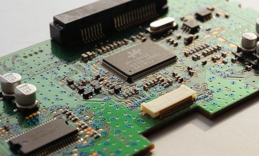
ADAS1000-4 ECG AFE: Pinout, Features and Datasheet


19 Bit 0.5mm AFE ADAS1000 3.3V 64-LQFP
The ADAS1000-4 is electro cardiac (ECG) front-end solution targeted at a variety of medical applications. The ADAS1000-4 is a full-featured, 3-channel ECG including respiration and pace detection. The ADAS1000-4 is designed to simplify the task of acquiring and ensuring quality ECG signals. Furthermore, Huge range of Semiconductors, Capacitors, Resistors and IcS in stock. Welcome RFQ.

What is ANALOG FRONT-END? What does ANALOG FRONT-END mean? ANALOG FRONT-END meaning & explanation
ADAS1000-4 Pinout

Pinout
ADAS1000-4 CAD Model

Symbol

Footprint
ADAS1000-4 Overview
The ADAS1000-4 is a full-featured, 3-channel ECG including respiration and pace detection. The ADAS1000-4 is designed to simplify the task of acquiring and ensuring quality ECG signals. It provides a low power, small data acquisition system for biopotential applications. Auxiliary features that aid in better quality ECG signal acquisition include: multichannel averaged driven lead, selectable reference drive, fast overload recovery, flexible respiration circuitry returning magnitude and phase information, internal pace detection algorithm operating on three leads, and the option of ac or dc lead-off detection. Several digital output options ensure flexibility when monitoring and analyzing signals. Value-added cardiac post processing is executed externally on a DSP, microprocessor, or FPGA. The ADAS1000-4 is available in two package options: either a 56-lead LFCSP or a 64-lead LQFP package; it is specified over −40°C to +85°C temperature range.
This article provides you with a basic overview of the ADAS1000-4 ECG Analog Front End, including its pin descriptions, features and specifications, etc., to help you quickly understand what ADAS1000-4 is.
ADAS1000-4 Features
● Biopotential signals in; digitized signals out
● 3 acquisition (ECG) channels and one driven lead
● Can be ganged for 8 electrode + RLD using master
● AC and DC lead-off detection
● Internal pace detection algorithm on 3 leads: Support for user’s own pace
● Thoracic impedance measurement (internal/external path)
● Selectable reference lead
● Scalable noise vs. power control, power-down modes
● Low power operation from: 11 mW (1 lead), 15 mW (3 leads)
● Lead or electrode data available
● Supports AAMI EC11:1991/(R)2001/(R)2007, AAMI EC38 R2007, EC13:2002/(R)2007, IEC60601-1 ed. 3.0 b:2005, IEC60601-2-25 ed. 2.0 :2011, IEC60601-2-27 ed. 2.0 b:2005, IEC60601-2-51 ed. 1.0 b: 2005
● Fast overload recovery
● Low or high speed data output rates
● Serial interface SPI-/QSPI™-/DSP-compatible
● 64-lead LQFP package (10 mm × 10 mm body size)
ADAS1000-4 Advantage
The ADAS1000-4 provides user programmable variables to optimize the performance of the algorithm within the ECG system, given all these limiting elements. The ADAS1000-4 has a high performance, low noise, on-chip 1.8 V reference for use in the ADC and DAC circuits. The ADAS1000-4 runs from an external crystal or clock input frequency of 8.192 MHz. The external clock input is provided for use in gang mode so conversions between the two devices are synchronized.
The ADAS1000-4 measures electro cardiac (ECG) signals, thoracic impedance, pacing artifacts, and lead-on/off status and output this information in the form of a data frame supplying either lead/vector or electrode data at programmable data rates. Its low power and small size make it suitable for portable, battery-powered applications. The high performance also makes it suitable for higher end diagnostic machines. Because ECG systems span different applications, the ADAS1000-4 features a power/noise scaling architecture where the noise can be reduced at the expense of increasing power consumption. Signal acquisition channels may be shut down to save power. Data rates can be reduced to save power. To ease manufacturing tests and development as well as offer holistic power-up testing, the ADAS1000-4 offers a suite of features, such as dc and ac test excitation via the calibration DAC and CRC redundancy testing in addition to readback of all relevant register address space. The input structure is a differential amplifier input thereby allowing users a variety of configuration options to best suit their application.
Specifications
- TypeParameter
- Factory Lead Time12 Weeks
- Lifecycle Status
Lifecycle Status refers to the current stage of an electronic component in its product life cycle, indicating whether it is active, obsolete, or transitioning between these states. An active status means the component is in production and available for purchase. An obsolete status indicates that the component is no longer being manufactured or supported, and manufacturers typically provide a limited time frame for support. Understanding the lifecycle status is crucial for design engineers to ensure continuity and reliability in their projects.
PRODUCTION (Last Updated: 3 weeks ago) - Surface Mount
having leads that are designed to be soldered on the side of a circuit board that the body of the component is mounted on.
YES - Package / Case
refers to the protective housing that encases an electronic component, providing mechanical support, electrical connections, and thermal management.
64-LQFP - Number of Pins64
- Packaging
Semiconductor package is a carrier / shell used to contain and cover one or more semiconductor components or integrated circuits. The material of the shell can be metal, plastic, glass or ceramic.
Tray - Pbfree Code
The "Pbfree Code" parameter in electronic components refers to the code or marking used to indicate that the component is lead-free. Lead (Pb) is a toxic substance that has been widely used in electronic components for many years, but due to environmental concerns, there has been a shift towards lead-free alternatives. The Pbfree Code helps manufacturers and users easily identify components that do not contain lead, ensuring compliance with regulations and promoting environmentally friendly practices. It is important to pay attention to the Pbfree Code when selecting electronic components to ensure they meet the necessary requirements for lead-free applications.
no - Part Status
Parts can have many statuses as they progress through the configuration, analysis, review, and approval stages.
Active - Moisture Sensitivity Level (MSL)
Moisture Sensitivity Level (MSL) is a standardized rating that indicates the susceptibility of electronic components, particularly semiconductors, to moisture-induced damage during storage and the soldering process, defining the allowable exposure time to ambient conditions before they require special handling or baking to prevent failures
3 (168 Hours) - Number of Terminations64
- ECCN Code
An ECCN (Export Control Classification Number) is an alphanumeric code used by the U.S. Bureau of Industry and Security to identify and categorize electronic components and other dual-use items that may require an export license based on their technical characteristics and potential for military use.
EAR99 - TypeGeneral Purpose
- Max Operating Temperature
The Maximum Operating Temperature is the maximum body temperature at which the thermistor is designed to operate for extended periods of time with acceptable stability of its electrical characteristics.
85°C - Min Operating Temperature
The "Min Operating Temperature" parameter in electronic components refers to the lowest temperature at which the component is designed to operate effectively and reliably. This parameter is crucial for ensuring the proper functioning and longevity of the component, as operating below this temperature may lead to performance issues or even damage. Manufacturers specify the minimum operating temperature to provide guidance to users on the environmental conditions in which the component can safely operate. It is important to adhere to this parameter to prevent malfunctions and ensure the overall reliability of the electronic system.
-40°C - Max Power Dissipation
The maximum power that the MOSFET can dissipate continuously under the specified thermal conditions.
29.7mW - Terminal Position
In electronic components, the term "Terminal Position" refers to the physical location of the connection points on the component where external electrical connections can be made. These connection points, known as terminals, are typically used to attach wires, leads, or other components to the main body of the electronic component. The terminal position is important for ensuring proper connectivity and functionality of the component within a circuit. It is often specified in technical datasheets or component specifications to help designers and engineers understand how to properly integrate the component into their circuit designs.
QUAD - Terminal Form
Occurring at or forming the end of a series, succession, or the like; closing; concluding.
GULL WING - Peak Reflow Temperature (Cel)
Peak Reflow Temperature (Cel) is a parameter that specifies the maximum temperature at which an electronic component can be exposed during the reflow soldering process. Reflow soldering is a common method used to attach electronic components to a circuit board. The Peak Reflow Temperature is crucial because it ensures that the component is not damaged or degraded during the soldering process. Exceeding the specified Peak Reflow Temperature can lead to issues such as component failure, reduced performance, or even permanent damage to the component. It is important for manufacturers and assemblers to adhere to the recommended Peak Reflow Temperature to ensure the reliability and functionality of the electronic components.
260 - Number of Functions1
- Supply Voltage
Supply voltage refers to the electrical potential difference provided to an electronic component or circuit. It is crucial for the proper operation of devices, as it powers their functions and determines performance characteristics. The supply voltage must be within specified limits to ensure reliability and prevent damage to components. Different electronic devices have specific supply voltage requirements, which can vary widely depending on their design and intended application.
3.3V - Terminal Pitch
The center distance from one pole to the next.
0.5mm - Time@Peak Reflow Temperature-Max (s)
Time@Peak Reflow Temperature-Max (s) refers to the maximum duration that an electronic component can be exposed to the peak reflow temperature during the soldering process, which is crucial for ensuring reliable solder joint formation without damaging the component.
30 - Base Part Number
The "Base Part Number" (BPN) in electronic components serves a similar purpose to the "Base Product Number." It refers to the primary identifier for a component that captures the essential characteristics shared by a group of similar components. The BPN provides a fundamental way to reference a family or series of components without specifying all the variations and specific details.
ADAS1000 - Pin Count
a count of all of the component leads (or pins)
64 - Operating Supply Voltage
The voltage level by which an electrical system is designated and to which certain operating characteristics of the system are related.
3.3V - Temperature Grade
Temperature grades represent a tire's resistance to heat and its ability to dissipate heat when tested under controlled laboratory test conditions.
INDUSTRIAL - Number of Channels4
- Interface
In electronic components, the term "Interface" refers to the point at which two different systems, devices, or components connect and interact with each other. It can involve physical connections such as ports, connectors, or cables, as well as communication protocols and standards that facilitate the exchange of data or signals between the connected entities. The interface serves as a bridge that enables seamless communication and interoperability between different parts of a system or between different systems altogether. Designing a reliable and efficient interface is crucial in ensuring proper functionality and performance of electronic components and systems.
SPI, Serial - Max Supply Voltage
In general, the absolute maximum common-mode voltage is VEE-0.3V and VCC+0.3V, but for products without a protection element at the VCC side, voltages up to the absolute maximum rated supply voltage (i.e. VEE+36V) can be supplied, regardless of supply voltage.
5.5V - Min Supply Voltage
The minimum supply voltage (V min ) is explored for sequential logic circuits by statistically simulating the impact of within-die process variations and gate-dielectric soft breakdown on data retention and hold time.
3.15V - Operating Supply Current
Operating Supply Current, also known as supply current or quiescent current, is a crucial parameter in electronic components that indicates the amount of current required for the device to operate under normal conditions. It represents the current drawn by the component from the power supply while it is functioning. This parameter is important for determining the power consumption of the component and is typically specified in datasheets to help designers calculate the overall power requirements of their circuits. Understanding the operating supply current is essential for ensuring proper functionality and efficiency of electronic systems.
5.4mA - Number of Bits19
- Common Mode Rejection Ratio
Common Mode Rejection Ratio (CMRR) is a measure of the ability of a differential amplifier to reject input signals that are common to both input terminals. It is defined as the ratio of the differential gain to the common mode gain. A high CMRR indicates that the amplifier can effectively eliminate noise and interference that affects both inputs simultaneously, enhancing the fidelity of the amplified signal. CMRR is typically expressed in decibels (dB), with higher values representing better performance in rejecting common mode signals.
110 dB - Max Input Voltage
Max Input Voltage refers to the maximum voltage level that an electronic component can safely handle without getting damaged. This parameter is crucial for ensuring the proper functioning and longevity of the component. Exceeding the specified maximum input voltage can lead to overheating, electrical breakdown, or permanent damage to the component. It is important to carefully adhere to the manufacturer's guidelines regarding the maximum input voltage to prevent any potential issues and maintain the reliability of the electronic device.
2.3V - Resolution
Resolution in electronic components refers to the smallest increment of measurement or change that can be detected or represented by the component. It is a crucial specification in devices such as sensors, displays, and converters, as it determines the level of detail or accuracy that can be achieved. For example, in a digital camera, resolution refers to the number of pixels that make up an image, with higher resolution indicating a greater level of detail. In analog-to-digital converters, resolution is the number of discrete values that can be represented in the digital output, determining the precision of the conversion process. Overall, resolution plays a significant role in determining the performance and capabilities of electronic components in various applications.
2.375 B - Voltage - Supply, Analog
Voltage - Supply, Analog is a parameter in electronic components that specifies the range of voltage levels required to power the analog circuitry within the component. This parameter indicates the minimum and maximum voltage levels that the component can accept for proper operation of its analog functions. It is crucial to ensure that the voltage supplied to the component falls within this specified range to prevent damage and ensure optimal performance. Understanding and adhering to the "Voltage - Supply, Analog" parameter is essential for the proper functioning of analog circuits in electronic components.
3.15V~5.5V - Voltage - Supply, Digital
Voltage - Supply, Digital is a parameter that specifies the voltage level required to power the digital circuitry within an electronic component, such as an integrated circuit or a microcontroller. This parameter is crucial for ensuring proper operation of the digital components, as supplying the correct voltage level is essential for reliable performance. The specified voltage range typically includes both minimum and maximum values within which the component can operate safely and efficiently. It is important to adhere to the recommended voltage supply range to prevent damage to the component and to maintain the integrity of the digital signals being processed.
1.71V~1.89V - Conversion Rate
the number of conversions divided by the total number of visitors.
2 Msps - Signal to Noise Ratio (SNR)
Signal to Noise Ratio (SNR) is a measure used in electronics to quantify the ratio of the strength of a desired signal to the strength of background noise. It is commonly expressed in decibels (dB) and is used to evaluate the quality of a signal transmission or processing system. A higher SNR indicates a stronger, clearer signal relative to the background noise, resulting in better performance and accuracy in electronic components such as amplifiers, receivers, and communication systems. SNR is crucial in ensuring reliable and efficient operation of electronic devices by minimizing the impact of unwanted noise on the signal quality.
100 dB - Width10.2mm
- Length10.2mm
- Height1.45mm
- RoHS Status
RoHS means “Restriction of Certain Hazardous Substances” in the “Hazardous Substances Directive” in electrical and electronic equipment.
ROHS3 Compliant - REACH SVHC
The parameter "REACH SVHC" in electronic components refers to the compliance with the Registration, Evaluation, Authorization, and Restriction of Chemicals (REACH) regulation regarding Substances of Very High Concern (SVHC). SVHCs are substances that may have serious effects on human health or the environment, and their use is regulated under REACH to ensure their safe handling and minimize their impact.Manufacturers of electronic components need to declare if their products contain any SVHCs above a certain threshold concentration and provide information on the safe use of these substances. This information allows customers to make informed decisions about the potential risks associated with using the components and take appropriate measures to mitigate any hazards.Ensuring compliance with REACH SVHC requirements is essential for electronics manufacturers to meet regulatory standards, protect human health and the environment, and maintain transparency in their supply chain. It also demonstrates a commitment to sustainability and responsible manufacturing practices in the electronics industry.
No SVHC - Lead Free
Lead Free is a term used to describe electronic components that do not contain lead as part of their composition. Lead is a toxic material that can have harmful effects on human health and the environment, so the electronics industry has been moving towards lead-free components to reduce these risks. Lead-free components are typically made using alternative materials such as silver, copper, and tin. Manufacturers must comply with regulations such as the Restriction of Hazardous Substances (RoHS) directive to ensure that their products are lead-free and environmentally friendly.
Contains Lead
ADAS1000-4 Functional Block Diagram

Simplified Block Diagram

Simplified Respiration Block Diagram

3-Channel Full Featured Model
Parts with Similar Specs
- ImagePart NumberManufacturerPackage / CaseNumber of PinsNumber of BitsInterfaceMin Supply VoltageSupply VoltageMax Supply VoltageNumber of TerminationsView Compare
![ADAS1000-4BSTZ]()
ADAS1000-4BSTZ
64-LQFP
64
19
SPI, Serial
3.15 V
3.3 V
5.5 V
64
![ADAS1000BSTZ]()
64-LQFP
64
16
Parallel, SPI
4.5 V
5 V
5.5 V
64
![AD7761BSTZ]()
64-LQFP
64
19
SPI, Serial
3.15 V
3.3 V
5.5 V
64
![ADS8557IPM]()
64-LQFP
64
14
Parallel, SPI
4.5 V
5 V
5.5 V
64
![ADS8556IPM]()
64-LQFP
64
16
-
2 V
5 V
5.5 V
64


ADAS1000-4 Applications
● ECG: monitor and diagnostic
● Bedside patient monitoring
● Portable telemetry
● Holter
● AED
● Cardiac defibrillators
● Ambulatory monitors
● Pace maker programmer
● Patient transport
● Stress testing
ADAS1000-4 Package

Package
ADAS1000-4 Manufacturer
Analog Devices (NASDAQ: ADI) is a world leader in the design, manufacture, and marketing of a broad portfolio of high performance analog, mixed-signal, and digital signal processing (DSP) integrated circuits (ICs) used in virtually all types of electronic equipment. Since our inception in 1965, we have focused on solving the engineering challenges associated with signal processing in electronic equipment. Used by over 100,000 customers worldwide, our signal processing products play a fundamental role in converting, conditioning, and processing real-world phenomena such as temperature, pressure, sound, light, speed, and motion into electrical signals to be used in a wide array of electronic devices.
Trend Analysis
Datasheet PDF
- Datasheets :
- PCN Assembly/Origin :
- PCN Design/Specification :
- ConflictMineralStatement :
What was the ADAS1000-4 designed for? Please elaborate briefly.
The ADAS1000-4 is designed to simplify the task of acquiring ECG signals for use in both monitor and diagnostic applications.
What are the components of the ADAS1000-4 ECG product?
The ADAS1000-4 ECG product consists of three ECG inputs and a reference drive, RLD (right leg drive).
What special methods are used to implement ADAS1000-4?
The ADAS1000-4 implementation uses a dccoupled approach, which requires that the front end be biased to operate within the limited dynamic range imposed by the relatively low supply voltage.
 P82B96 Bipolar IC: Pinout, 3D Model and Datasheet
02 November 20212842
 A Comprehensive Guide to LTC7001IMSE#TRPBF PMIC Gate Driver
06 March 2024752
 MIC29302WU Voltage Regulator: Pinout, Applications and Datasheet
24 October 20232318
 1N4001 vs. 1N4148: Which one is better?
23 February 20227335
 SP2526A USB Power Distribution Switch: Pinout, Equivalent and Datasheet
15 March 2022594
 CP0402W2700FNTR Coupler: Features, Applications and Datasheet
14 August 2024309
 LM393 - Low Offset Voltage Dual Comparator IC
02 December 202113939
 TIP120 vs TIP122 Darlington NPN Transistor
29 July 202210232
 Devices based on Semiconductor Laser Chaos for Optical Communications
22 February 20232366
 Kyoto University Successfully Demonstrates That SiC Can Also Work at 350°C
26 March 2022753
 Tough Times for Japanese Component Manufacturers
10 August 20222958
 Detailed Introduction of the Chip Design Process
21 December 202118041
 What is SPI (Serial Perripheral Interface)?
25 November 20215044
 Commonly Used Circuit Protection Components: How to Match the Right Device to Each Threat
30 June 20266382
 An Analysis of Low Pressure on Partial Discharge in Micro-Voids in Aviation
25 January 20242292
 Designing Application-Specific Integrated Circuits
07 March 20252277
Analog Devices Inc.
In Stock: 2
Minimum: 1 Multiples: 1
Qty
Unit Price
Ext Price
1
$34.243769
$34.24
10
$32.305442
$323.05
100
$30.476833
$3,047.68
500
$28.751729
$14,375.86
1000
$27.124272
$27,124.27
Not the price you want? Send RFQ Now and we'll contact you ASAP.
Inquire for More Quantity
![AD7730BRUZ]() AD7730BRUZ
AD7730BRUZAnalog Devices Inc.
![AD7730BRUZ-REEL7]() AD7730BRUZ-REEL7
AD7730BRUZ-REEL7Analog Devices Inc.
![ADAS1000BSTZ]() ADAS1000BSTZ
ADAS1000BSTZAnalog Devices Inc.
![AD7730BRZ]() AD7730BRZ
AD7730BRZAnalog Devices Inc.
![AD7730BRZ-REEL]() AD7730BRZ-REEL
AD7730BRZ-REELAnalog Devices Inc.
![AD7195BCPZ]() AD7195BCPZ
AD7195BCPZAnalog Devices Inc.
![AD73311ARSZ]() AD73311ARSZ
AD73311ARSZAnalog Devices Inc.
![ADAS1000-2BSTZ]() ADAS1000-2BSTZ
ADAS1000-2BSTZAnalog Devices Inc.
![AD73360ARZ]() AD73360ARZ
AD73360ARZAnalog Devices Inc.
![ADAS1000BCPZ]() ADAS1000BCPZ
ADAS1000BCPZAnalog Devices Inc.


