
 Product
 Brand
Brand Articles
 Tools
Tools
2N2222A NPN Transistor: Datasheet, Pinout and Equivalents


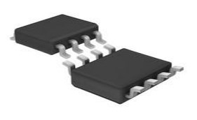
TRANS NPN 40V 0.8A TO-18
2N2222A is a npn silicon switching transistor. This article mainly covers datasheet, pinout, equivalent and other details about 2N2222A.

2 Simple 2n2222a electronic projects
2N2222A Pinout

2N2222A Pinout

2N222A Description
2N2222A is an NPN transistor hence the collector and emitter will be left open (Reverse biased) when the base pin is held at the ground and will be closed (Forward biased) when a signal is provided to the base pin. 2N2222A has a gain value of 110 to 800, this value determines the amplification capacity of the transistor.
2N2222A CAD Model
Symbol

2N2222A Symbol
Footprint

2N2222A Footprint
Specifications
- TypeParameter
- Factory Lead Time8 Weeks
- Mount
In electronic components, the term "Mount" typically refers to the method or process of physically attaching or fixing a component onto a circuit board or other electronic device. This can involve soldering, adhesive bonding, or other techniques to secure the component in place. The mounting process is crucial for ensuring proper electrical connections and mechanical stability within the electronic system. Different components may have specific mounting requirements based on their size, shape, and function, and manufacturers provide guidelines for proper mounting procedures to ensure optimal performance and reliability of the electronic device.
Through Hole - Package / Case
refers to the protective housing that encases an electronic component, providing mechanical support, electrical connections, and thermal management.
TO-18 - Number of Pins3
- Collector-Emitter Breakdown Voltage40V
- Collector-Emitter Saturation Voltage1V
- Frequency(Max)300MHz
- Number of Elements1
- Power Dissipation (Max)500mW
- hFEMin100
- Packaging
Semiconductor package is a carrier / shell used to contain and cover one or more semiconductor components or integrated circuits. The material of the shell can be metal, plastic, glass or ceramic.
Bulk - Published2003
- JESD-609 Code
The "JESD-609 Code" in electronic components refers to a standardized marking code that indicates the lead-free solder composition and finish of electronic components for compliance with environmental regulations.
e0 - Pbfree Code
The "Pbfree Code" parameter in electronic components refers to the code or marking used to indicate that the component is lead-free. Lead (Pb) is a toxic substance that has been widely used in electronic components for many years, but due to environmental concerns, there has been a shift towards lead-free alternatives. The Pbfree Code helps manufacturers and users easily identify components that do not contain lead, ensuring compliance with regulations and promoting environmentally friendly practices. It is important to pay attention to the Pbfree Code when selecting electronic components to ensure they meet the necessary requirements for lead-free applications.
no - Part Status
Parts can have many statuses as they progress through the configuration, analysis, review, and approval stages.
Active - Number of Terminations3
- ECCN Code
An ECCN (Export Control Classification Number) is an alphanumeric code used by the U.S. Bureau of Industry and Security to identify and categorize electronic components and other dual-use items that may require an export license based on their technical characteristics and potential for military use.
EAR99 - Terminal Finish
Terminal Finish refers to the surface treatment applied to the terminals or leads of electronic components to enhance their performance and longevity. It can improve solderability, corrosion resistance, and overall reliability of the connection in electronic assemblies. Common finishes include nickel, gold, and tin, each possessing distinct properties suitable for various applications. The choice of terminal finish can significantly impact the durability and effectiveness of electronic devices.
Tin/Lead (Sn/Pb) - Max Operating Temperature
The Maximum Operating Temperature is the maximum body temperature at which the thermistor is designed to operate for extended periods of time with acceptable stability of its electrical characteristics.
200°C - Min Operating Temperature
The "Min Operating Temperature" parameter in electronic components refers to the lowest temperature at which the component is designed to operate effectively and reliably. This parameter is crucial for ensuring the proper functioning and longevity of the component, as operating below this temperature may lead to performance issues or even damage. Manufacturers specify the minimum operating temperature to provide guidance to users on the environmental conditions in which the component can safely operate. It is important to adhere to this parameter to prevent malfunctions and ensure the overall reliability of the electronic system.
-65°C - Terminal Position
In electronic components, the term "Terminal Position" refers to the physical location of the connection points on the component where external electrical connections can be made. These connection points, known as terminals, are typically used to attach wires, leads, or other components to the main body of the electronic component. The terminal position is important for ensuring proper connectivity and functionality of the component within a circuit. It is often specified in technical datasheets or component specifications to help designers and engineers understand how to properly integrate the component into their circuit designs.
BOTTOM - Terminal Form
Occurring at or forming the end of a series, succession, or the like; closing; concluding.
WIRE - Frequency
In electronic components, the parameter "Frequency" refers to the rate at which a signal oscillates or cycles within a given period of time. It is typically measured in Hertz (Hz) and represents how many times a signal completes a full cycle in one second. Frequency is a crucial aspect in electronic components as it determines the behavior and performance of various devices such as oscillators, filters, and communication systems. Understanding the frequency characteristics of components is essential for designing and analyzing electronic circuits to ensure proper functionality and compatibility with other components in a system.
250MHz - Pin Count
a count of all of the component leads (or pins)
3 - Polarity
In electronic components, polarity refers to the orientation or direction in which the component must be connected in a circuit to function properly. Components such as diodes, capacitors, and LEDs have polarity markings to indicate which terminal should be connected to the positive or negative side of the circuit. Connecting a component with incorrect polarity can lead to malfunction or damage. It is important to pay attention to polarity markings and follow the manufacturer's instructions to ensure proper operation of electronic components.
NPN - Element Configuration
The distribution of electrons of an atom or molecule (or other physical structure) in atomic or molecular orbitals.
Single - Power Dissipation
the process by which an electronic or electrical device produces heat (energy loss or waste) as an undesirable derivative of its primary action.
500mW - Transistor Application
In the context of electronic components, the parameter "Transistor Application" refers to the specific purpose or function for which a transistor is designed and used. Transistors are semiconductor devices that can amplify or switch electronic signals and are commonly used in various electronic circuits. The application of a transistor can vary widely depending on its design and characteristics, such as whether it is intended for audio amplification, digital logic, power control, or radio frequency applications. Understanding the transistor application is important for selecting the right type of transistor for a particular circuit or system to ensure optimal performance and functionality.
SWITCHING - Gain Bandwidth Product
The gain–bandwidth product (designated as GBWP, GBW, GBP, or GB) for an amplifier is the product of the amplifier's bandwidth and the gain at which the bandwidth is measured.
300MHz - Collector Emitter Voltage (VCEO)
Collector-Emitter Voltage (VCEO) is a key parameter in electronic components, particularly in transistors. It refers to the maximum voltage that can be applied between the collector and emitter terminals of a transistor while the base terminal is open or not conducting. Exceeding this voltage limit can lead to breakdown and potential damage to the transistor. VCEO is crucial for ensuring the safe and reliable operation of the transistor within its specified limits. Designers must carefully consider VCEO when selecting transistors for a circuit to prevent overvoltage conditions that could compromise the performance and longevity of the component.
40V - Max Collector Current
Max Collector Current is a parameter used to specify the maximum amount of current that can safely flow through the collector terminal of a transistor or other electronic component without causing damage. It is typically expressed in units of amperes (A) and is an important consideration when designing circuits to ensure that the component operates within its safe operating limits. Exceeding the specified max collector current can lead to overheating, degradation of performance, or even permanent damage to the component. Designers must carefully consider this parameter when selecting components and designing circuits to ensure reliable and safe operation.
800mA - Transition Frequency
Transition Frequency in electronic components refers to the frequency at which a device can transition from one state to another, typically defining the upper limit of its operating frequency. It is a critical parameter in determining the speed and performance of active components like transistors and integrated circuits. This frequency is influenced by factors such as capacitance, resistance, and the inherent characteristics of the materials used in the component's construction. Understanding transition frequency is essential for optimizing circuit designs and ensuring reliable signal processing in various applications.
300MHz - Frequency - Transition
The parameter "Frequency - Transition" in electronic components refers to the maximum frequency at which a signal transition can occur within the component. It is a crucial specification for digital circuits as it determines the speed at which data can be processed and transmitted. A higher frequency transition allows for faster operation and better performance of the electronic component. It is typically measured in hertz (Hz) or megahertz (MHz) and is specified by the manufacturer to ensure proper functioning of the component within a given frequency range.
300MHz - Collector Base Voltage (VCBO)
Collector Base Voltage (VCBO) is the maximum allowable voltage that can be applied between the collector and base terminals of a bipolar junction transistor when the emitter is open. It is a critical parameter that determines the voltage rating of the transistor and helps prevent breakdown in the collector-base junction. Exceeding this voltage can lead to permanent damage or failure of the component.
75V - Emitter Base Voltage (VEBO)
Emitter Base Voltage (VEBO) is a parameter used in electronic components, particularly in transistors. It refers to the maximum voltage that can be applied between the emitter and base terminals of a transistor without causing damage to the device. Exceeding this voltage limit can lead to breakdown of the transistor and potential failure. VEBO is an important specification to consider when designing circuits to ensure the proper operation and reliability of the components. It is typically provided in the datasheet of the transistor and should be carefully observed to prevent any potential damage during operation.
6V - DC Current Gain-Min (hFE)
The parameter "DC Current Gain-Min (hFE)" in electronic components refers to the minimum value of the DC current gain of a bipolar junction transistor (BJT). It is a measure of how much the transistor amplifies the input current to produce the output current. The hFE value indicates the ratio of the output current to the input current when the transistor is operating in the active region. A higher hFE value signifies a higher current gain and better amplification capabilities of the transistor. It is an important parameter to consider when designing and analyzing transistor circuits for various electronic applications.
40 - Max Junction Temperature (Tj)
Max Junction Temperature (Tj) refers to the maximum allowable temperature at the junction of a semiconductor device, such as a transistor or integrated circuit. It is a critical parameter that influences the performance, reliability, and lifespan of the component. Exceeding this temperature can lead to thermal runaway, breakdown, or permanent damage to the device. Proper thermal management is essential to ensure the junction temperature remains within safe operating limits during device operation.
200°C - Turn Off Time-Max (toff)
The parameter "Turn Off Time-Max (toff)" in electronic components refers to the maximum time taken for a device to switch from an ON state to an OFF state. It is a crucial specification in devices such as transistors, diodes, and other semiconductor components that control the flow of current. The turn-off time is important for determining the switching speed and efficiency of a component, as a shorter turn-off time generally indicates faster operation and reduced power losses. Designers and engineers use this parameter to ensure proper functioning and performance of electronic circuits and systems.
285ns - Height5.33mm
- Radiation Hardening
Radiation hardening is the process of making electronic components and circuits resistant to damage or malfunction caused by high levels of ionizing radiation, especially for environments in outer space (especially beyond the low Earth orbit), around nuclear reactors and particle accelerators, or during nuclear accidents or nuclear warfare.
No - RoHS Status
RoHS means “Restriction of Certain Hazardous Substances” in the “Hazardous Substances Directive” in electrical and electronic equipment.
RoHS Compliant - Lead Free
Lead Free is a term used to describe electronic components that do not contain lead as part of their composition. Lead is a toxic material that can have harmful effects on human health and the environment, so the electronics industry has been moving towards lead-free components to reduce these risks. Lead-free components are typically made using alternative materials such as silver, copper, and tin. Manufacturers must comply with regulations such as the Restriction of Hazardous Substances (RoHS) directive to ensure that their products are lead-free and environmentally friendly.
Lead Free
2N2222A Features
High current (max.800mA)
Low voltage (max.40V)
Lead Free Finish/RoHS Complaint
2N2222A Equivalents
2N2222A Applications
Can be used to switch large current (up to 800mA) loads
Can be used in a variety of switching applications
Can be used in Darlington pairs
Motors speed control
Inverters and other rectifier circuits
Can be used in Darlington pairs
Where to use 2N2222A
2N2222A can allow collector current up to 800mA and also has a power dissipation of 652mW which can be used to drive large loads. And if you are looking for an NPN transistor that could switch loads of higher current, 2N2222A might the right choice for your project.
How to use 2N2222A
2N2222A NPN transistor can be used either as a switch or as an amplifier. The Base-Emitter voltage of this transistor is 6V so you just have to supply this voltage across the base and emitter of the transistor to induce a base current into the transistor. This transistor will make it forward biased and thus closes the connection between collector and emitter. However, one important thing to notice is the Base resistor. This resistor will limit the current flowing through the transistor to prevent it from damaging. The value for this resistor can be calculated using the formula.
2N2222A Application Circuit
To make things simple I have shown a simplified circuit to make a transistor as a switch. In the actual circuit, modifications might be required. I have used a base voltage of 5V and a value of 1K as a current limiting resistor.

2N2222A Application Circuit
2N2222A Dimension


2N2222A Manufacturer
Since 1974, Central Semiconductor has manufactured innovative discrete semiconductors used in electronic products worldwide. Devices currently include standard and custom small-signal transistors, bipolar power transistors, MOSFETs, diodes, rectifiers, protection devices, current limiting diodes, bridge rectifiers, thyristors, and silicon carbide devices. Central’s devices are available in industry-standard surface mount and through-hole packages, bare die, TLMs (Tiny Leadless Modules™), and MDMs (Multi Discrete Modules™). Central has earned a reputation as a manufacturer of the highest quality products consistently delivered on time, and a provider of exceptional value-added services.
Trend Analysis
Datasheet PDF
- Datasheets :
- ReachStatement :
Is there a 2N2222 SMD equivalent?
2N3904(PNP), 2N2907(PNP), 2N3906 (PNP) are complementary transistor pairs.
What is the 2N2222 current Beta gain?
Answer: DC Current Gain (hfe) - 100 to 300
How do I connect a 2N2222 to Arduino?
Your transistor is backwards. The reason you are getting 4.7 volts is because of the PN junction between the base and emitter in the transistor. When D8 is high, this junction is forward biased and drops about 0.7 volts.
What is diffrence between transistor 2N2222A and F2222A?
The 2N2222 is used for general purpose low-power amplifying or switching applications. It is designed for low to medium current, low power, medium voltage, and can operate at moderately high speeds. Frequently used as small signal transisitor
F2222A is a small load switch transistor with high gain and low saturation voltage .
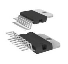 TDA7293 DMOS Audio Amplifier: Datasheet, TDA7293 vs. TDA7294
03 December 202116541
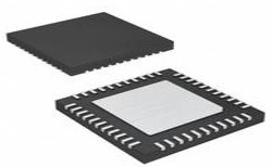
 Understanding the STM32H750VBT6 Microcontroller
24 July 20251131
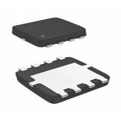 AON7410 30V N-Channel MOSFET, AON7410 Equivalents
18 February 20225114
 A Comprehensive Guide to LTC6952IUKG#TRPBF Clock Generator by Linear Technology/Analog Devices
06 March 2024312
 1N4742A Zener Diodes: Features, Pinout, and Datasheet
18 October 20218875
 ATMEGA32U4 Microcontroller: Pinout, Datasheet and Equivalents
09 July 202113748
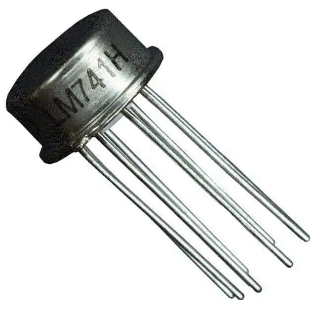 LM741H Operational Amplifier: Pinout, Datasheet, and Functional Block Diagram
27 July 20216457
 LT1054 Voltage Converter and Regulator: Pinout, Applications and Datasheet
03 November 20214345
 What is Visible Light Communication(VLC)?
13 October 202115575
 Challenges and Control Approaches for Current Sharing in DC Microgrids
07 June 20235151
 Analyzing the Latest Electronic Components Trends and Their Functions 2023 – 2024
21 July 20252864
 Low-Power Design of Operational Amplifiers
27 March 20256953
 Real-time Cloud Analytics in Semiconductor Manufacturing
01 November 20222695
 Unveiling the Potential of GaN Semiconductor-Enabled Three-Phase Propulsion Inverters for Enhanced EV Performance
09 August 20231627
 Essential Tips for Picking the Best Gas Sensor
15 July 20252854
 Introduction to Flash Memory
31 October 20259230
Central Semiconductor
In Stock: 147
United States
China
Canada
Japan
Russia
Germany
United Kingdom
Singapore
Italy
Hong Kong(China)
Taiwan(China)
France
Korea
Mexico
Netherlands
Malaysia
Austria
Spain
Switzerland
Poland
Thailand
Vietnam
India
United Arab Emirates
Afghanistan
Åland Islands
Albania
Algeria
American Samoa
Andorra
Angola
Anguilla
Antigua & Barbuda
Argentina
Armenia
Aruba
Australia
Azerbaijan
Bahamas
Bahrain
Bangladesh
Barbados
Belarus
Belgium
Belize
Benin
Bermuda
Bhutan
Bolivia
Bonaire, Sint Eustatius and Saba
Bosnia & Herzegovina
Botswana
Brazil
British Indian Ocean Territory
British Virgin Islands
Brunei
Bulgaria
Burkina Faso
Burundi
Cabo Verde
Cambodia
Cameroon
Cayman Islands
Central African Republic
Chad
Chile
Christmas Island
Cocos (Keeling) Islands
Colombia
Comoros
Congo
Congo (DRC)
Cook Islands
Costa Rica
Côte d’Ivoire
Croatia
Cuba
Curaçao
Cyprus
Czechia
Denmark
Djibouti
Dominica
Dominican Republic
Ecuador
Egypt
El Salvador
Equatorial Guinea
Eritrea
Estonia
Eswatini
Ethiopia
Falkland Islands
Faroe Islands
Fiji
Finland
French Guiana
French Polynesia
Gabon
Gambia
Georgia
Ghana
Gibraltar
Greece
Greenland
Grenada
Guadeloupe
Guam
Guatemala
Guernsey
Guinea
Guinea-Bissau
Guyana
Haiti
Honduras
Hungary
Iceland
Indonesia
Iran
Iraq
Ireland
Isle of Man
Israel
Jamaica
Jersey
Jordan
Kazakhstan
Kenya
Kiribati
Kosovo
Kuwait
Kyrgyzstan
Laos
Latvia
Lebanon
Lesotho
Liberia
Libya
Liechtenstein
Lithuania
Luxembourg
Macao(China)
Madagascar
Malawi
Maldives
Mali
Malta
Marshall Islands
Martinique
Mauritania
Mauritius
Mayotte
Micronesia
Moldova
Monaco
Mongolia
Montenegro
Montserrat
Morocco
Mozambique
Myanmar
Namibia
Nauru
Nepal
New Caledonia
New Zealand
Nicaragua
Niger
Nigeria
Niue
Norfolk Island
North Korea
North Macedonia
Northern Mariana Islands
Norway
Oman
Pakistan
Palau
Palestinian Authority
Panama
Papua New Guinea
Paraguay
Peru
Philippines
Pitcairn Islands
Portugal
Puerto Rico
Qatar
Réunion
Romania
Rwanda
Samoa
San Marino
São Tomé & Príncipe
Saudi Arabia
Senegal
Serbia
Seychelles
Sierra Leone
Sint Maarten
Slovakia
Slovenia
Solomon Islands
Somalia
South Africa
South Sudan
Sri Lanka
St Helena, Ascension, Tristan da Cunha
St. Barthélemy
St. Kitts & Nevis
St. Lucia
St. Martin
St. Pierre & Miquelon
St. Vincent & Grenadines
Sudan
Suriname
Svalbard & Jan Mayen
Sweden
Syria
Tajikistan
Tanzania
Timor-Leste
Togo
Tokelau
Tonga
Trinidad & Tobago
Tunisia
Turkey
Turkmenistan
Turks & Caicos Islands
Tuvalu
U.S. Outlying Islands
U.S. Virgin Islands
Uganda
Ukraine
Uruguay
Uzbekistan
Vanuatu
Vatican City
Venezuela
Wallis & Futuna
Yemen
Zambia
Zimbabwe
![MPSA66 TIN/LEAD]() MPSA66 TIN/LEAD
MPSA66 TIN/LEADCentral Semiconductor
![MPSA77 APP TIN/LEAD]() MPSA77 APP TIN/LEAD
MPSA77 APP TIN/LEADCentral Semiconductor
![MM3007 TIN/LEAD]() MM3007 TIN/LEAD
MM3007 TIN/LEADCentral Semiconductor
![MPS3704 PBFREE]() MPS3704 PBFREE
MPS3704 PBFREECentral Semiconductor
![MPS6531 PBFREE]() MPS6531 PBFREE
MPS6531 PBFREECentral Semiconductor
![2N3505 TIN/LEAD]() 2N3505 TIN/LEAD
2N3505 TIN/LEADCentral Semiconductor
![2N2907A]() 2N2907A
2N2907ACentral Semiconductor
![2N4910 PBFREE]() 2N4910 PBFREE
2N4910 PBFREECentral Semiconductor
![2N2222A PBFREE]() 2N2222A PBFREE
2N2222A PBFREECentral Semiconductor Corp
![PN3569 TIN/LEAD]() PN3569 TIN/LEAD
PN3569 TIN/LEADCentral Semiconductor


