
 Product
 Brand
Brand Articles
 Tools
Tools
A Comprehensive Guide to the 5962-8851301GA Linear Amplifier: Features, Applications, and Reference Designs


80pA 86 dB Instrumentational OP Amps 0.0002μA ±8V~20V OP42 8 Pins TO-99-8 Metal Can
In this article, we will explore the 5962-8851301GA linear amplifier, a versatile electronic component manufactured by Analog Devices Inc. We will delve into its features, applications, reference designs, and alternative parts. Whether you are an electronic engineer or a hobbyist, this guide will provide you with valuable insights into this product.
Product Introduction
1. Description:
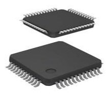
The 5962-8851301GA is a voltage-feedback amplifier designed for instrumentation and operational amplifier applications. It comes in a TO-99-8 metal can package with 8 pins and can operate in a wide temperature range of -55°C to 125°C. This amplifier offers high performance, reliability, and precision, making it suitable for various electronic systems.
2. Features:
- J-FET architecture: The amplifier utilizes J-FET technology, ensuring low input bias current and high input impedance.
- Wide supply voltage range: It can operate with a single or dual supply voltage ranging from ±8V to ±20V, providing flexibility in different system configurations.
- High gain bandwidth product: With a gain bandwidth product of 10MHz, this amplifier can handle high-frequency signals accurately.
- Low offset voltage: The input offset voltage is as low as 1mV, minimizing errors in precision applications.
- High slew rate: The amplifier offers a slew rate of 52V/μs, enabling it to respond quickly to fast-changing input signals.
- Low power consumption: It has a low current supply of 5.1mA, making it suitable for power-sensitive applications.
- Frequency compensation: The amplifier features frequency compensation, ensuring stability and preventing oscillations in feedback systems.
3. Applications:
Primary Applications:
- Test and measurement equipment: The 5962-8851301GA is ideal for use in oscilloscopes, signal generators, spectrum analyzers, and other precision measurement instruments.
- Data acquisition systems: It can be used in data acquisition systems to amplify and condition signals from various sensors and transducers.
- Audio equipment: The amplifier is suitable for audio amplification, including preamplifiers, headphone amplifiers, and audio mixers.
- Industrial control systems: It finds applications in industrial control systems, such as motor control, robotics, and process control.
- Medical devices: The amplifier can be utilized in medical equipment like patient monitoring systems, ECG amplifiers, and medical imaging devices.
Secondary Applications:
- Communication systems: It can be employed in communication systems, including radio frequency (RF) amplifiers and baseband amplification stages.
- Automotive electronics: The amplifier can be utilized in automotive electronics, such as audio systems, sensor interfaces, and control modules.
Applicable Specific Modules:
- Analog Devices offers various evaluation boards and development kits that incorporate the 5962-8851301GA amplifier. These modules provide a convenient platform for testing and prototyping in specific applications.
4. Reference Designs:
- Analog Devices provides several reference designs that utilize the 5962-8851301GA amplifier. These reference designs serve as valuable resources for engineers and designers looking to implement the amplifier in their projects. Some examples include audio amplifiers, precision voltage references, and sensor signal conditioning circuits.
5. Alternative Parts:
- While the 5962-8851301GA amplifier is a reliable and widely used component, there are alternative parts available in the market. Some alternatives to consider include the AD8671, AD8672, and OP27 amplifiers, which offer similar features and performance characteristics.
6. FAQs:
Q1: Is the 5962-8851301GA amplifier RoHS compliant?
A1: No, this amplifier is non-RoHS compliant and contains lead.
Q2: Can the 5962-8851301GA amplifier withstand radiation?
A2: No, this amplifier is not radiation-hardened.
Q3: What is the maximum power dissipation of the 5962-8851301GA amplifier?
A3: The maximum power dissipation is 500mW.
Q4: Is the 5962-8851301GA amplifier available in surface mount packages?
A4: No, it is only available in a TO-99-8 metal can package.
Q5: Can the 5962-8851301GA amplifier operate with a single supply voltage?
A5: Yes, it can operate with a single supply voltage ranging from +8V to +20V.
In conclusion, the 5962-8851301GA linear amplifier offers a range of features that make it suitable for various applications in instrumentation, operational amplifiers, and other electronic systems. Its high performance, reliability, and precision make it a popular choice among engineers and designers. With the availability of reference designs and alternative parts, users have the flexibility to incorporate this amplifier into their projects effectively.
Specifications
- TypeParameter
- Lifecycle Status
Lifecycle Status refers to the current stage of an electronic component in its product life cycle, indicating whether it is active, obsolete, or transitioning between these states. An active status means the component is in production and available for purchase. An obsolete status indicates that the component is no longer being manufactured or supported, and manufacturers typically provide a limited time frame for support. Understanding the lifecycle status is crucial for design engineers to ensure continuity and reliability in their projects.
PRODUCTION (Last Updated: 1 week ago) - Factory Lead Time12 Weeks
- Contact Plating
Contact plating (finish) provides corrosion protection for base metals and optimizes the mechanical and electrical properties of the contact interfaces.
Lead, Tin - Mount
In electronic components, the term "Mount" typically refers to the method or process of physically attaching or fixing a component onto a circuit board or other electronic device. This can involve soldering, adhesive bonding, or other techniques to secure the component in place. The mounting process is crucial for ensuring proper electrical connections and mechanical stability within the electronic system. Different components may have specific mounting requirements based on their size, shape, and function, and manufacturers provide guidelines for proper mounting procedures to ensure optimal performance and reliability of the electronic device.
Through Hole - Mounting Type
The "Mounting Type" in electronic components refers to the method used to attach or connect a component to a circuit board or other substrate, such as through-hole, surface-mount, or panel mount.
Through Hole - Package / Case
refers to the protective housing that encases an electronic component, providing mechanical support, electrical connections, and thermal management.
TO-99-8 Metal Can - Number of Pins8
- Number of Elements1
- Usage LevelMilitary grade
- Operating Temperature
The operating temperature is the range of ambient temperature within which a power supply, or any other electrical equipment, operate in. This ranges from a minimum operating temperature, to a peak or maximum operating temperature, outside which, the power supply may fail.
-55°C~125°C - Packaging
Semiconductor package is a carrier / shell used to contain and cover one or more semiconductor components or integrated circuits. The material of the shell can be metal, plastic, glass or ceramic.
Tube - Series
In electronic components, the "Series" refers to a group of products that share similar characteristics, designs, or functionalities, often produced by the same manufacturer. These components within a series typically have common specifications but may vary in terms of voltage, power, or packaging to meet different application needs. The series name helps identify and differentiate between various product lines within a manufacturer's catalog.
Military, MIL-STD-883 - JESD-609 Code
The "JESD-609 Code" in electronic components refers to a standardized marking code that indicates the lead-free solder composition and finish of electronic components for compliance with environmental regulations.
e0 - Pbfree Code
The "Pbfree Code" parameter in electronic components refers to the code or marking used to indicate that the component is lead-free. Lead (Pb) is a toxic substance that has been widely used in electronic components for many years, but due to environmental concerns, there has been a shift towards lead-free alternatives. The Pbfree Code helps manufacturers and users easily identify components that do not contain lead, ensuring compliance with regulations and promoting environmentally friendly practices. It is important to pay attention to the Pbfree Code when selecting electronic components to ensure they meet the necessary requirements for lead-free applications.
no - Part Status
Parts can have many statuses as they progress through the configuration, analysis, review, and approval stages.
Active - Moisture Sensitivity Level (MSL)
Moisture Sensitivity Level (MSL) is a standardized rating that indicates the susceptibility of electronic components, particularly semiconductors, to moisture-induced damage during storage and the soldering process, defining the allowable exposure time to ambient conditions before they require special handling or baking to prevent failures
1 (Unlimited) - Number of Terminations8
- ECCN Code
An ECCN (Export Control Classification Number) is an alphanumeric code used by the U.S. Bureau of Industry and Security to identify and categorize electronic components and other dual-use items that may require an export license based on their technical characteristics and potential for military use.
EAR99 - Terminal Finish
Terminal Finish refers to the surface treatment applied to the terminals or leads of electronic components to enhance their performance and longevity. It can improve solderability, corrosion resistance, and overall reliability of the connection in electronic assemblies. Common finishes include nickel, gold, and tin, each possessing distinct properties suitable for various applications. The choice of terminal finish can significantly impact the durability and effectiveness of electronic devices.
Tin/Lead (Sn63Pb37) - Max Power Dissipation
The maximum power that the MOSFET can dissipate continuously under the specified thermal conditions.
500mW - Terminal Position
In electronic components, the term "Terminal Position" refers to the physical location of the connection points on the component where external electrical connections can be made. These connection points, known as terminals, are typically used to attach wires, leads, or other components to the main body of the electronic component. The terminal position is important for ensuring proper connectivity and functionality of the component within a circuit. It is often specified in technical datasheets or component specifications to help designers and engineers understand how to properly integrate the component into their circuit designs.
BOTTOM - Terminal Form
Occurring at or forming the end of a series, succession, or the like; closing; concluding.
WIRE - Number of Functions1
- Supply Voltage
Supply voltage refers to the electrical potential difference provided to an electronic component or circuit. It is crucial for the proper operation of devices, as it powers their functions and determines performance characteristics. The supply voltage must be within specified limits to ensure reliability and prevent damage to components. Different electronic devices have specific supply voltage requirements, which can vary widely depending on their design and intended application.
15V - Base Part Number
The "Base Part Number" (BPN) in electronic components serves a similar purpose to the "Base Product Number." It refers to the primary identifier for a component that captures the essential characteristics shared by a group of similar components. The BPN provides a fundamental way to reference a family or series of components without specifying all the variations and specific details.
OP42 - Pin Count
a count of all of the component leads (or pins)
8 - Qualification Status
An indicator of formal certification of qualifications.
Qualified - Power Dissipation
the process by which an electronic or electrical device produces heat (energy loss or waste) as an undesirable derivative of its primary action.
500mW - Current - Supply
Current - Supply is a parameter in electronic components that refers to the maximum amount of electrical current that the component can provide to the circuit it is connected to. It is typically measured in units of amperes (A) and is crucial for determining the power handling capability of the component. Understanding the current supply rating is important for ensuring that the component can safely deliver the required current without overheating or failing. It is essential to consider this parameter when designing circuits to prevent damage to the component and ensure proper functionality of the overall system.
5.1mA - Slew Rate
the maximum rate of output voltage change per unit time.
52V/μs - Architecture
In electronic components, the parameter "Architecture" refers to the overall design and structure of the component. It encompasses the arrangement of internal components, the layout of circuitry, and the physical form of the component. The architecture of an electronic component plays a crucial role in determining its functionality, performance, and compatibility with other components in a system. Different architectures can result in variations in power consumption, speed, size, and other key characteristics of the component. Designers often consider the architecture of electronic components carefully to ensure optimal performance and integration within a larger system.
VOLTAGE-FEEDBACK - Amplifier Type
Amplifier Type refers to the classification or categorization of amplifiers based on their design, functionality, and characteristics. Amplifiers are electronic devices that increase the amplitude of a signal, such as voltage or current. The type of amplifier determines its specific application, performance capabilities, and operating characteristics. Common types of amplifiers include operational amplifiers (op-amps), power amplifiers, audio amplifiers, and radio frequency (RF) amplifiers. Understanding the amplifier type is crucial for selecting the right component for a particular circuit or system design.
J-FET - Common Mode Rejection Ratio
Common Mode Rejection Ratio (CMRR) is a measure of the ability of a differential amplifier to reject input signals that are common to both input terminals. It is defined as the ratio of the differential gain to the common mode gain. A high CMRR indicates that the amplifier can effectively eliminate noise and interference that affects both inputs simultaneously, enhancing the fidelity of the amplified signal. CMRR is typically expressed in decibels (dB), with higher values representing better performance in rejecting common mode signals.
86 dB - Current - Input Bias
The parameter "Current - Input Bias" in electronic components refers to the amount of current required at the input terminal of a device to maintain proper operation. It is a crucial specification as it determines the minimum input current needed for the component to function correctly. Input bias current can affect the performance and accuracy of the device, especially in precision applications where small signal levels are involved. It is typically specified in datasheets for operational amplifiers, transistors, and other semiconductor devices to provide users with important information for circuit design and analysis.
80pA - Voltage - Supply, Single/Dual (±)
The parameter "Voltage - Supply, Single/Dual (±)" in electronic components refers to the power supply voltage required for the proper operation of the component. This parameter indicates whether the component requires a single power supply voltage (e.g., 5V) or a dual power supply voltage (e.g., ±15V). For components that require a single power supply voltage, only one voltage level is needed for operation. On the other hand, components that require a dual power supply voltage need both positive and negative voltage levels to function correctly.Understanding the voltage supply requirements of electronic components is crucial for designing and integrating them into circuits to ensure proper functionality and prevent damage due to incorrect voltage levels.
±8V~20V - Input Offset Voltage (Vos)
Input Offset Voltage (Vos) is a key parameter in electronic components, particularly in operational amplifiers. It refers to the voltage difference that must be applied between the two input terminals of the amplifier to nullify the output voltage when the input terminals are shorted together. In simpler terms, it represents the voltage required to bring the output of the amplifier to zero when there is no input signal present. Vos is an important parameter as it can introduce errors in the output signal of the amplifier, especially in precision applications where accuracy is crucial. Minimizing Vos is essential to ensure the amplifier operates with high precision and accuracy.
1mV - Gain Bandwidth Product
The gain–bandwidth product (designated as GBWP, GBW, GBP, or GB) for an amplifier is the product of the amplifier's bandwidth and the gain at which the bandwidth is measured.
10MHz - Neg Supply Voltage-Nom (Vsup)
The parameter "Neg Supply Voltage-Nom (Vsup)" in electronic components refers to the nominal negative supply voltage that the component requires to operate within its specified performance characteristics. This parameter indicates the minimum voltage level that must be provided to the component's negative supply pin for proper functionality. It is important to ensure that the negative supply voltage provided to the component does not exceed the maximum specified value to prevent damage or malfunction. Understanding and adhering to the specified negative supply voltage requirements is crucial for the reliable operation of the electronic component in a circuit.
-15V - Unity Gain BW-Nom
Unity Gain Bandwidth, often abbreviated as Unity Gain BW or UGBW, refers to the frequency at which an amplifier can provide a gain of one (0 dB). It is a critical parameter in assessing the performance of operational amplifiers and other amplifying devices, indicating the range of frequencies over which the amplifier can operate without distortion. Unity Gain BW is particularly important in applications where signal fidelity is crucial, as it helps determine the maximum frequency of operation for a given gain level. As the gain is reduced, the bandwidth typically increases, ensuring that the amplifier can still operate effectively across various signal frequencies.
10000 kHz - Voltage Gain
Voltage gain is a measure of how much an electronic component or circuit amplifies an input voltage signal to produce an output voltage signal. It is typically expressed as a ratio or in decibels (dB). A higher voltage gain indicates a greater amplification of the input signal. Voltage gain is an important parameter in amplifiers, where it determines the level of amplification provided by the circuit. It is calculated by dividing the output voltage by the input voltage and is a key factor in determining the overall performance and functionality of electronic devices.
119.08dB - Average Bias Current-Max (IIB)
The parameter "Average Bias Current-Max (IIB)" in electronic components refers to the maximum average bias current that the component can handle without exceeding its specified operating limits. Bias current is the current that flows through a component when it is in its quiescent state or when it is not actively processing a signal. Exceeding the maximum average bias current can lead to overheating, reduced performance, or even damage to the component. Therefore, it is important to ensure that the bias current does not exceed the specified maximum value to maintain the reliability and longevity of the electronic component.
0.0002μA - Power Supply Rejection Ratio (PSRR)
Power Supply Rejection Ratio (PSRR) is a measure of how well an electronic component, such as an operational amplifier or voltage regulator, can reject changes in its supply voltage. It indicates the ability of the component to maintain a stable output voltage despite fluctuations in the input supply voltage. A higher PSRR value signifies better performance in rejecting noise and variations from the power supply, leading to improved signal integrity and more reliable operation in electronic circuits. PSRR is typically expressed in decibels (dB).
100.92dB - Low-Offset
Low-offset is a parameter used to describe the level of offset voltage in electronic components, particularly in operational amplifiers. Offset voltage refers to the small voltage difference that exists between the input terminals of the amplifier when the input voltage is zero. A low-offset value indicates that this voltage difference is minimal, which is desirable for accurate signal processing and amplification. Components with low-offset specifications are preferred in applications where precision and accuracy are critical, such as in instrumentation and measurement systems. Minimizing offset voltage helps reduce errors and ensures the faithful reproduction of input signals by the amplifier.
NO - Frequency Compensation
Frequency compensation is implemented by modifying the gain and phase characteristics of the amplifier's open loop output or of its feedback network, or both, in such a way as to avoid the conditions leading to oscillation. This is usually done by the internal or external use of resistance-capacitance networks.
YES - Supply Voltage Limit-Max
The parameter "Supply Voltage Limit-Max" in electronic components refers to the maximum voltage that the component can safely handle without getting damaged. This specification is crucial for ensuring the reliable operation and longevity of the component within a given electrical system. Exceeding the maximum supply voltage limit can lead to overheating, electrical breakdown, or permanent damage to the component. It is important to carefully adhere to this limit when designing and operating electronic circuits to prevent potential failures and ensure the overall system's performance and safety.
20V - Voltage - Input Offset
Voltage - Input Offset is a parameter that refers to the difference in voltage between the input terminals of an electronic component, such as an operational amplifier, when the input voltage is zero. It is an important characteristic that can affect the accuracy and performance of the component in various applications. A low input offset voltage is desirable as it indicates that the component will have minimal error in its output when the input signal is near zero. Manufacturers typically provide this specification in the component's datasheet to help users understand the component's behavior and make informed decisions when designing circuits.
300μV - Low-Bias
Low-bias in electronic components refers to a design or configuration that minimizes the amount of bias current flowing through the component. Bias current is a small, steady current that is used to establish the operating point of a component, such as a transistor or amplifier. By reducing the bias current to a low level, the component can operate with lower power consumption and potentially lower distortion. Low-bias components are often used in applications where power efficiency and signal fidelity are important, such as in audio amplifiers or battery-powered devices. Overall, the low-bias parameter indicates the ability of the component to operate efficiently and accurately with minimal bias current.
YES - Bias Current-Max (IIB) @25C
The parameter "Bias Current-Max (IIB) @25C" in electronic components refers to the maximum input bias current that the component can handle at a specified temperature of 25 degrees Celsius. Bias current is the current flowing into the input terminal of a device when no signal is applied. This parameter is important because excessive bias current can affect the performance and stability of the component, leading to potential issues such as distortion or offset errors in the output signal. By specifying the maximum bias current allowed at a certain temperature, manufacturers provide users with important information to ensure proper operation and reliability of the component in their circuit designs.
0.0002μA - Dual Supply Voltage
Dual Supply Voltage refers to an electronic component's requirement for two separate power supply voltages, typically one positive and one negative. This configuration is commonly used in operational amplifiers, analog circuits, and certain digital devices to allow for greater signal handling capabilities and improved performance. The use of dual supply voltages enables the device to process bipolar signals, thereby enhancing its functionality in various applications.
15V - Neg Supply Voltage-Max (Vsup)
Neg Supply Voltage-Max (Vsup) refers to the maximum negative supply voltage that an electronic component can tolerate without being damaged. It indicates the lowest voltage level that can be applied to the negative supply pin of the device. Exceeding this parameter can lead to functional failure or permanent damage to the component. This specification is crucial for ensuring proper operation and preventing circuit malfunction in designs that utilize negative voltage supplies.
-20V - Radiation Hardening
Radiation hardening is the process of making electronic components and circuits resistant to damage or malfunction caused by high levels of ionizing radiation, especially for environments in outer space (especially beyond the low Earth orbit), around nuclear reactors and particle accelerators, or during nuclear accidents or nuclear warfare.
No - RoHS Status
RoHS means “Restriction of Certain Hazardous Substances” in the “Hazardous Substances Directive” in electrical and electronic equipment.
Non-RoHS Compliant - Lead Free
Lead Free is a term used to describe electronic components that do not contain lead as part of their composition. Lead is a toxic material that can have harmful effects on human health and the environment, so the electronics industry has been moving towards lead-free components to reduce these risks. Lead-free components are typically made using alternative materials such as silver, copper, and tin. Manufacturers must comply with regulations such as the Restriction of Hazardous Substances (RoHS) directive to ensure that their products are lead-free and environmentally friendly.
Contains Lead
Parts with Similar Specs
- ImagePart NumberManufacturerPackage / CaseNumber of PinsSlew RateGain Bandwidth ProductInput Offset Voltage (Vos)Power Supply Rejection Ratio (PSRR)Common Mode Rejection RatioSupply VoltageView Compare
![5962-8851301GA]()
5962-8851301GA
TO-99-8 Metal Can
8
52V/μs
10MHz
1 mV
100.92 dB
86 dB
15 V
![LM741H/NOPB]()
TO-99-8 Metal Can
8
0.5V/μs
1.5MHz
1 mV
77 dB
70 dB
15 V
![OPA128JM]()
TO-99-8 Metal Can
8
3V/μs
-
1 mV
80 dB
80 dB
15 V
![OP42EJ]()
TO-99-8 Metal Can
8
58V/μs
10MHz
750 μV
100.92 dB
92 dB
15 V


Datasheet PDF
- Datasheets :
- PCN Assembly/Origin :
- ConflictMineralStatement :
 SX1276 Transceiver: Datasheet, SX1276 vs. SX1272
09 November 202116890
 STM32F091CC Microcontroller: Features, Pinout, and Datasheet
13 January 20223231
![2N3904 Silicon NPN Transistor[FAQ]:Datasheet, Pinout, Equivalent and Package](https://res.utmel.com/Images/Article/e1bcb6c2-6f0d-489f-a0e2-86d3984cd2d9.jpg) 2N3904 Silicon NPN Transistor[FAQ]:Datasheet, Pinout, Equivalent and Package
2N3904 Silicon NPN Transistor[FAQ]:Datasheet, Pinout, Equivalent and Package06 April 202213535
 PIC24FJ128GB204 Microcontroller Datasheet Overview
29 February 2024128
 A Comprehensive Guide to LTC7103IUHE#TRPBF DC-DC Switching Regulator
06 March 2024227
 LTM8062IV#PBF Battery Charger: A Comprehensive Technical Overview
06 March 2024142
 TIP110 NPN Power Darlington Transistor: Pinout, Datasheet pdf and Equivalent
18 December 20213206
 An In-depth Look at LTC7003IMSE#TRPBF Gate Driver: Features, Applications, and Reference Designs
06 March 2024355
 Exploring the Advancements in Storage Technologies and Grid Architecture of Electric Vehicle Charging Systems
18 October 20232516
 What is Amplifier?
08 November 20257979
 Electronic Components Distributor Utmel to Showcase at 2024 IPC APEX EXPO
10 April 20245894
 HBM4 and the Shift to Customized AI Memory: The Advanced Packaging Bottleneck
22 June 20261290
 Why Your Power Supply Ripple Is So Big?
18 March 20225594
 Why RFID Technology Matters for Retail Innovation Today
10 July 20252747
 2 Semiconductor Stocks to Buy Hand Over Fist in 2024 and 1 to Avoid Like the Plague
18 December 20234356
 Various Reasons for the Failure, Explosion and Burning of Tantalum Capacitors
02 June 202211324
Analog Devices Inc.
In Stock: 2722
United States
China
Canada
Japan
Russia
Germany
United Kingdom
Singapore
Italy
Hong Kong(China)
Taiwan(China)
France
Korea
Mexico
Netherlands
Malaysia
Austria
Spain
Switzerland
Poland
Thailand
Vietnam
India
United Arab Emirates
Afghanistan
Åland Islands
Albania
Algeria
American Samoa
Andorra
Angola
Anguilla
Antigua & Barbuda
Argentina
Armenia
Aruba
Australia
Azerbaijan
Bahamas
Bahrain
Bangladesh
Barbados
Belarus
Belgium
Belize
Benin
Bermuda
Bhutan
Bolivia
Bonaire, Sint Eustatius and Saba
Bosnia & Herzegovina
Botswana
Brazil
British Indian Ocean Territory
British Virgin Islands
Brunei
Bulgaria
Burkina Faso
Burundi
Cabo Verde
Cambodia
Cameroon
Cayman Islands
Central African Republic
Chad
Chile
Christmas Island
Cocos (Keeling) Islands
Colombia
Comoros
Congo
Congo (DRC)
Cook Islands
Costa Rica
Côte d’Ivoire
Croatia
Cuba
Curaçao
Cyprus
Czechia
Denmark
Djibouti
Dominica
Dominican Republic
Ecuador
Egypt
El Salvador
Equatorial Guinea
Eritrea
Estonia
Eswatini
Ethiopia
Falkland Islands
Faroe Islands
Fiji
Finland
French Guiana
French Polynesia
Gabon
Gambia
Georgia
Ghana
Gibraltar
Greece
Greenland
Grenada
Guadeloupe
Guam
Guatemala
Guernsey
Guinea
Guinea-Bissau
Guyana
Haiti
Honduras
Hungary
Iceland
Indonesia
Iran
Iraq
Ireland
Isle of Man
Israel
Jamaica
Jersey
Jordan
Kazakhstan
Kenya
Kiribati
Kosovo
Kuwait
Kyrgyzstan
Laos
Latvia
Lebanon
Lesotho
Liberia
Libya
Liechtenstein
Lithuania
Luxembourg
Macao(China)
Madagascar
Malawi
Maldives
Mali
Malta
Marshall Islands
Martinique
Mauritania
Mauritius
Mayotte
Micronesia
Moldova
Monaco
Mongolia
Montenegro
Montserrat
Morocco
Mozambique
Myanmar
Namibia
Nauru
Nepal
New Caledonia
New Zealand
Nicaragua
Niger
Nigeria
Niue
Norfolk Island
North Korea
North Macedonia
Northern Mariana Islands
Norway
Oman
Pakistan
Palau
Palestinian Authority
Panama
Papua New Guinea
Paraguay
Peru
Philippines
Pitcairn Islands
Portugal
Puerto Rico
Qatar
Réunion
Romania
Rwanda
Samoa
San Marino
São Tomé & Príncipe
Saudi Arabia
Senegal
Serbia
Seychelles
Sierra Leone
Sint Maarten
Slovakia
Slovenia
Solomon Islands
Somalia
South Africa
South Sudan
Sri Lanka
St Helena, Ascension, Tristan da Cunha
St. Barthélemy
St. Kitts & Nevis
St. Lucia
St. Martin
St. Pierre & Miquelon
St. Vincent & Grenadines
Sudan
Suriname
Svalbard & Jan Mayen
Sweden
Syria
Tajikistan
Tanzania
Timor-Leste
Togo
Tokelau
Tonga
Trinidad & Tobago
Tunisia
Turkey
Turkmenistan
Turks & Caicos Islands
Tuvalu
U.S. Outlying Islands
U.S. Virgin Islands
Uganda
Ukraine
Uruguay
Uzbekistan
Vanuatu
Vatican City
Venezuela
Wallis & Futuna
Yemen
Zambia
Zimbabwe
![AD826AR-REEL7]() AD826AR-REEL7
AD826AR-REEL7Analog Devices Inc.
![AD8062ARM]() AD8062ARM
AD8062ARMAnalog Devices Inc.
![AD8532ARU-REEL]() AD8532ARU-REEL
AD8532ARU-REELAnalog Devices Inc.
![OP113ES]() OP113ES
OP113ESAnalog Devices Inc.
![SSM2142P]() SSM2142P
SSM2142PAnalog Devices, Inc.
![LTC1050CS8]() LTC1050CS8
LTC1050CS8Linear Technology/Analog Devices
![AMP02EPZ]() AMP02EPZ
AMP02EPZAnalog Devices Inc.
![AD822ARZ-REEL7]() AD822ARZ-REEL7
AD822ARZ-REEL7Analog Devices Inc.
![OP2177ARZ-REEL7]() OP2177ARZ-REEL7
OP2177ARZ-REEL7Analog Devices Inc.
![AD8066ARZ-R7]() AD8066ARZ-R7
AD8066ARZ-R7Analog Devices Inc.


