
 Product
 Brand
Brand Articles
 Tools
Tools
AD584 Precision Voltage Reference: Pinout, Features and Datasheet [FAQ]

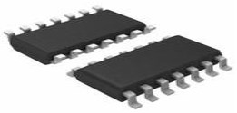
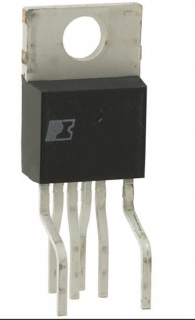
0°C~70°C TA Programmable 2.54mm PMIC AD584 1 Channel 15V 8-DIP (0.300, 7.62mm)
Unit Price: $37.439633
Ext Price: $37.44


0°C~70°C TA Programmable 2.54mm PMIC AD584 1 Channel 15V 8-DIP (0.300, 7.62mm)
The AD584 is an 8-terminal precision voltage reference offering pin programmable selection of four popular output voltages: 10.000 V, 7.500 V, 5.000 V and 2.500 V. This article will introduce AD584 systematically from its features, pinout to its specifications, CAD Models, also including AD584 datasheet and so much more. Furthermore, Huge range of Semiconductors, Capacitors, Resistors and IcS in stock. Welcome RFQ.

Scullcom Hobby Electronics #8 - Precision Voltage Reference Modules
AD584 Pinout
The following figure is the diagram of AD584 Pinout.

Pinout
AD584 CAD Models
The followings are AD584 Symbol, Footprint, and 3D Model.

PCB Symbol

PCB Footprint

3D Model
AD584 Description
The AD584 is an 8-terminal precision voltage reference offering pin programmable selection of four popular output voltages: 10.000 V, 7.500 V, 5.000 V and 2.500 V. Other output voltages, above, below, or between the four standard outputs, are available by the addition of external resistors. The input voltage can vary between 4.5 V and 30 V.
Laser wafer trimming (LWT) is used to adjust the pin programmable output levels and temperature coefficients, resulting in the most flexible high precision voltage reference available in monolithic form.
In addition to the programmable output voltages, the AD584 offers a unique strobe terminal that permits the device to be turned on or off. When the AD584 is used as a power supply reference, the supply can be switched off with a single, low power signal. In the off state, the current drained by the AD584 is reduced to approximately 100 µA. In the on state, the total supply current is typically 750 µA, including the output buffer amplifier.
The AD584 is recommended for use as a reference for 8-, 10-, or 12-bit digital-to-analog converters (DACs) that require an external precision reference. In addition, the device is ideal for analog-to-digital converters (ADCs) of up to 14-bit accuracy, either successive approximation or integrating designs, and in general, it can offer better performance than that provided by standard self-contained references.
The AD584J and AD584K are specified for operation from 0°C to +70°C, and the AD584S and AD584T are specified for the −55°C to +125°C range. All grades are packaged in a hermetically sealed, eight-terminal TO-99 metal can, and the AD584J and AD584K are also available in an 8-lead PDIP.
AD584 Product Highlights
1. The flexibility of the AD584 eliminates the need to design-in and inventory several different voltage references. Furthermore, one AD584 can serve as several references simultaneously when buffered properly.
2. Laser trimming of both initial accuracy and temperature coefficient results in very low errors overtemperature without the use of external components.
3. The AD584 can be operated in a 2-terminal Zener mode at a 5 V output and above. By connecting the input and the output, the AD584 can be used in this Zener configuration as a negative reference.
4. The output of the AD584 is configured to sink or source currents. This means that small reverse currents can be tolerated in circuits using the AD584 without damage to the reference and without disturbing the output voltage(10 V, 7.5 V, and 5 V outputs).
5. The AD584 is available in versions compliant with MIL-STD-883. Refer to the Analog Devices current AD584/883B data sheet for detailed specifications. This can be found under the Additional Data Sheetssection of the AD584 product page.
AD584 Features
● Four programmable output voltages
● 10.000 V, 7.500 V, 5.000 V, and 2.500 V
● Laser-trimmed to high accuracies
● No external components required
● Trimmed temperature coefficient: 15 ppm/°C maximum, 0°C to 70°C (AD584K)
● Zero output strobe terminal provided
● 2-terminal negative reference: capability (5 V and above)
● Output sources or sinks current
● Low quiescent current: 1.0 mA maximum
● 10 mA current output capability
● MIL-STD-883 compliant versions available
Specifications
- TypeParameter
- Lifecycle Status
Lifecycle Status refers to the current stage of an electronic component in its product life cycle, indicating whether it is active, obsolete, or transitioning between these states. An active status means the component is in production and available for purchase. An obsolete status indicates that the component is no longer being manufactured or supported, and manufacturers typically provide a limited time frame for support. Understanding the lifecycle status is crucial for design engineers to ensure continuity and reliability in their projects.
PRODUCTION (Last Updated: 2 weeks ago) - Factory Lead Time8 Weeks
- Mounting Type
The "Mounting Type" in electronic components refers to the method used to attach or connect a component to a circuit board or other substrate, such as through-hole, surface-mount, or panel mount.
Through Hole - Package / Case
refers to the protective housing that encases an electronic component, providing mechanical support, electrical connections, and thermal management.
8-DIP (0.300, 7.62mm) - Surface Mount
having leads that are designed to be soldered on the side of a circuit board that the body of the component is mounted on.
NO - Number of Pins8
- Operating Temperature
The operating temperature is the range of ambient temperature within which a power supply, or any other electrical equipment, operate in. This ranges from a minimum operating temperature, to a peak or maximum operating temperature, outside which, the power supply may fail.
0°C~70°C TA - Packaging
Semiconductor package is a carrier / shell used to contain and cover one or more semiconductor components or integrated circuits. The material of the shell can be metal, plastic, glass or ceramic.
Tube - Tolerance
In electronic components, "tolerance" refers to the acceptable deviation or variation from the specified or ideal value of a particular parameter, such as resistance, capacitance, or voltage. It indicates the range within which the actual value of the component can fluctuate while still being considered acceptable for use in a circuit. Tolerance is typically expressed as a percentage or a specific value and is important for ensuring the accuracy and reliability of electronic devices. Components with tighter tolerances are more precise but may also be more expensive. It is crucial to consider tolerance when selecting components to ensure proper functionality and performance of the circuit.
±0.1% - JESD-609 Code
The "JESD-609 Code" in electronic components refers to a standardized marking code that indicates the lead-free solder composition and finish of electronic components for compliance with environmental regulations.
e3 - Pbfree Code
The "Pbfree Code" parameter in electronic components refers to the code or marking used to indicate that the component is lead-free. Lead (Pb) is a toxic substance that has been widely used in electronic components for many years, but due to environmental concerns, there has been a shift towards lead-free alternatives. The Pbfree Code helps manufacturers and users easily identify components that do not contain lead, ensuring compliance with regulations and promoting environmentally friendly practices. It is important to pay attention to the Pbfree Code when selecting electronic components to ensure they meet the necessary requirements for lead-free applications.
no - Part Status
Parts can have many statuses as they progress through the configuration, analysis, review, and approval stages.
Active - Moisture Sensitivity Level (MSL)
Moisture Sensitivity Level (MSL) is a standardized rating that indicates the susceptibility of electronic components, particularly semiconductors, to moisture-induced damage during storage and the soldering process, defining the allowable exposure time to ambient conditions before they require special handling or baking to prevent failures
1 (Unlimited) - Number of Terminations8
- ECCN Code
An ECCN (Export Control Classification Number) is an alphanumeric code used by the U.S. Bureau of Industry and Security to identify and categorize electronic components and other dual-use items that may require an export license based on their technical characteristics and potential for military use.
EAR99 - Temperature Coefficient
The resistance-change factor per degree Celsius of temperature change is called the temperature coefficient of resistance. This factor is represented by the Greek lower-case letter “alpha” (α). A positive coefficient for a material means that its resistance increases with an increase in temperature.
15ppm/°C - Terminal Finish
Terminal Finish refers to the surface treatment applied to the terminals or leads of electronic components to enhance their performance and longevity. It can improve solderability, corrosion resistance, and overall reliability of the connection in electronic assemblies. Common finishes include nickel, gold, and tin, each possessing distinct properties suitable for various applications. The choice of terminal finish can significantly impact the durability and effectiveness of electronic devices.
Matte Tin (Sn) - Terminal Position
In electronic components, the term "Terminal Position" refers to the physical location of the connection points on the component where external electrical connections can be made. These connection points, known as terminals, are typically used to attach wires, leads, or other components to the main body of the electronic component. The terminal position is important for ensuring proper connectivity and functionality of the component within a circuit. It is often specified in technical datasheets or component specifications to help designers and engineers understand how to properly integrate the component into their circuit designs.
DUAL - Number of Functions1
- Supply Voltage
Supply voltage refers to the electrical potential difference provided to an electronic component or circuit. It is crucial for the proper operation of devices, as it powers their functions and determines performance characteristics. The supply voltage must be within specified limits to ensure reliability and prevent damage to components. Different electronic devices have specific supply voltage requirements, which can vary widely depending on their design and intended application.
15V - Terminal Pitch
The center distance from one pole to the next.
2.54mm - Base Part Number
The "Base Part Number" (BPN) in electronic components serves a similar purpose to the "Base Product Number." It refers to the primary identifier for a component that captures the essential characteristics shared by a group of similar components. The BPN provides a fundamental way to reference a family or series of components without specifying all the variations and specific details.
AD584 - Pin Count
a count of all of the component leads (or pins)
8 - Number of Outputs3
- Output Voltage
Output voltage is a crucial parameter in electronic components that refers to the voltage level produced by the component as a result of its operation. It represents the electrical potential difference between the output terminal of the component and a reference point, typically ground. The output voltage is a key factor in determining the performance and functionality of the component, as it dictates the level of voltage that will be delivered to the connected circuit or load. It is often specified in datasheets and technical specifications to ensure compatibility and proper functioning within a given system.
10V - Output Type
The "Output Type" parameter in electronic components refers to the type of signal or data that is produced by the component as an output. This parameter specifies the nature of the output signal, such as analog or digital, and can also include details about the voltage levels, current levels, frequency, and other characteristics of the output signal. Understanding the output type of a component is crucial for ensuring compatibility with other components in a circuit or system, as well as for determining how the output signal can be utilized or processed further. In summary, the output type parameter provides essential information about the nature of the signal that is generated by the electronic component as its output.
Programmable - Max Output Current
The maximum current that can be supplied to the load.
10mA - Supply Voltage-Max (Vsup)
The parameter "Supply Voltage-Max (Vsup)" in electronic components refers to the maximum voltage that can be safely applied to the component without causing damage. It is an important specification to consider when designing or using electronic circuits to ensure the component operates within its safe operating limits. Exceeding the maximum supply voltage can lead to overheating, component failure, or even permanent damage. It is crucial to adhere to the specified maximum supply voltage to ensure the reliable and safe operation of the electronic component.
30V - Number of Channels1
- Trim/Adjustable Output
Trim or adjustable output refers to the ability of an electronic component, such as a voltage regulator or power supply, to produce an output voltage that can be finely tuned or adjusted to meet specific requirements. This feature allows for precise control over the output voltage level, accommodating variations in load conditions or desired operational parameters. Users can typically achieve this adjustment through external resistors, potentiometers, or internal calibration mechanisms, ensuring optimal performance in diverse applications.
YES - Analog IC - Other Type
Analog IC - Other Type is a parameter used to categorize electronic components that are integrated circuits (ICs) designed for analog signal processing but do not fall into more specific subcategories such as amplifiers, comparators, or voltage regulators. These ICs may include specialized analog functions such as analog-to-digital converters (ADCs), digital-to-analog converters (DACs), voltage references, or signal conditioning circuits. They are typically used in various applications where precise analog signal processing is required, such as in audio equipment, instrumentation, communication systems, and industrial control systems. Manufacturers provide detailed specifications for these components to help engineers select the most suitable IC for their specific design requirements.
THREE TERMINAL VOLTAGE REFERENCE - Operating Supply Current
Operating Supply Current, also known as supply current or quiescent current, is a crucial parameter in electronic components that indicates the amount of current required for the device to operate under normal conditions. It represents the current drawn by the component from the power supply while it is functioning. This parameter is important for determining the power consumption of the component and is typically specified in datasheets to help designers calculate the overall power requirements of their circuits. Understanding the operating supply current is essential for ensuring proper functionality and efficiency of electronic systems.
1mA - Nominal Supply Current
Nominal current is the same as the rated current. It is the current drawn by the motor while delivering rated mechanical output at its shaft.
750μA - Max Supply Current
Max Supply Current refers to the maximum amount of electrical current that a component can draw from its power supply under normal operating conditions. It is a critical parameter that ensures the component operates reliably without exceeding its thermal limits or damaging internal circuitry. Exceeding this current can lead to overheating, performance degradation, or failure of the component. Understanding this parameter is essential for designing circuits that provide adequate power while avoiding overload situations.
1mA - Quiescent Current
The quiescent current is defined as the current level in the amplifier when it is producing an output of zero.
1mA - Voltage - Output (Min/Fixed)
Voltage - Output (Min/Fixed) refers to the minimum fixed output voltage level that an electronic component, such as a voltage regulator or power supply, is designed to provide under specified load conditions. This parameter ensures that the device consistently delivers a reliable voltage that meets the requirements of the connected circuits or components. It is critical for applications where stable and predictable voltage is necessary for proper operation.
2.5V 5V 7.5V 10V - Min Input Voltage
The parameter "Min Input Voltage" in electronic components refers to the minimum voltage level that must be applied to the component for it to operate within its specified parameters. This value is crucial as providing a voltage below this minimum threshold may result in the component malfunctioning or not functioning at all. It is important to adhere to the specified minimum input voltage to ensure the proper operation and longevity of the electronic component. Failure to meet this requirement may lead to potential damage to the component or the overall system in which it is used.
4.5V - Max Input Voltage
Max Input Voltage refers to the maximum voltage level that an electronic component can safely handle without getting damaged. This parameter is crucial for ensuring the proper functioning and longevity of the component. Exceeding the specified maximum input voltage can lead to overheating, electrical breakdown, or permanent damage to the component. It is important to carefully adhere to the manufacturer's guidelines regarding the maximum input voltage to prevent any potential issues and maintain the reliability of the electronic device.
40V - Reference Voltage
A voltage reference is an electronic device that ideally produces a fixed (constant) voltage irrespective of the loading on the device, power supply variations, temperature changes, and the passage of time. Voltage references are used in power supplies, analog-to-digital converters, digital-to-analog converters, and other measurement and control systems. Voltage references vary widely in performance; a regulator for a computer power supply may only hold its value to within a few percent of the nominal value, whereas laboratory voltage standards have precisions and stability measured in parts per million.
10V - Reference Type
a code object that is not stored directly where it is created, but that acts as a kind of pointer to a value stored elsewhere.
Series - Noise - 0.1Hz to 10Hz
In electronic components, the parameter "Noise - 0.1Hz to 10Hz" refers to the level of unwanted electrical signals or fluctuations present within that specific frequency range. This noise can interfere with the desired signals passing through the component, affecting the overall performance and accuracy of the electronic system. The measurement is typically expressed in units such as microvolts or decibels and indicates the amount of random variations or disturbances within the specified frequency band. Lower values of noise in this frequency range are desirable for high-quality electronic components and circuits, as they help ensure better signal integrity and reliability.
50μVp-p - Height3.3mm
- Length9.91mm
- Width6.35mm
- REACH SVHC
The parameter "REACH SVHC" in electronic components refers to the compliance with the Registration, Evaluation, Authorization, and Restriction of Chemicals (REACH) regulation regarding Substances of Very High Concern (SVHC). SVHCs are substances that may have serious effects on human health or the environment, and their use is regulated under REACH to ensure their safe handling and minimize their impact.Manufacturers of electronic components need to declare if their products contain any SVHCs above a certain threshold concentration and provide information on the safe use of these substances. This information allows customers to make informed decisions about the potential risks associated with using the components and take appropriate measures to mitigate any hazards.Ensuring compliance with REACH SVHC requirements is essential for electronics manufacturers to meet regulatory standards, protect human health and the environment, and maintain transparency in their supply chain. It also demonstrates a commitment to sustainability and responsible manufacturing practices in the electronics industry.
No SVHC - Radiation Hardening
Radiation hardening is the process of making electronic components and circuits resistant to damage or malfunction caused by high levels of ionizing radiation, especially for environments in outer space (especially beyond the low Earth orbit), around nuclear reactors and particle accelerators, or during nuclear accidents or nuclear warfare.
No - RoHS Status
RoHS means “Restriction of Certain Hazardous Substances” in the “Hazardous Substances Directive” in electrical and electronic equipment.
ROHS3 Compliant - Lead Free
Lead Free is a term used to describe electronic components that do not contain lead as part of their composition. Lead is a toxic material that can have harmful effects on human health and the environment, so the electronics industry has been moving towards lead-free components to reduce these risks. Lead-free components are typically made using alternative materials such as silver, copper, and tin. Manufacturers must comply with regulations such as the Restriction of Hazardous Substances (RoHS) directive to ensure that their products are lead-free and environmentally friendly.
Contains Lead
AD584 Functional Block Diagram
The following is the Schematic Diagram of AD584.

Schematic Diagram
Parts with Similar Specs
- ImagePart NumberManufacturerPackage / CaseNumber of PinsMax Output CurrentMin Input VoltageMax Input VoltageOutput VoltageToleranceTemperature CoefficientView Compare
![AD584KNZ]()
AD584KNZ
8-DIP (0.300, 7.62mm)
8
10 mA
4.5 V
40 V
10 V
±0.1%
15ppm/°C
![AD586KNZ]()
8-DIP (0.300, 7.62mm)
8
10 mA
4.5 V
40 V
10 V
±0.3%
30ppm/°C
![REF03GPZ]()
8-DIP (0.300, 7.62mm)
8
10 mA
10.8 V
36 V
5 V
±0.1%
15ppm/°C
![AD584JNZ]()
8-DIP (0.300, 7.62mm)
8
10 mA
4.5 V
40 V
2.5 V
±0.6%
50ppm/°C

AD584 Package
The following diagrams show the AD584 Package.

View A

View B

View C
AD584 Manufacturer
Analog Devices (NASDAQ: ADI) is a world leader in the design, manufacture, and marketing of a broad portfolio of high performance analog, mixed-signal, and digital signal processing (DSP) integrated circuits (ICs) used in virtually all types of electronic equipment. Since our inception in 1965, we have focused on solving the engineering challenges associated with signal processing in electronic equipment. Used by over 100,000 customers worldwide, our signal processing products play a fundamental role in converting, conditioning, and processing real-world phenomena such as temperature, pressure, sound, light, speed, and motion into electrical signals to be used in a wide array of electronic devices.
Datasheet PDF
- Datasheets :
- ConflictMineralStatement :
How many pins of AD584KNZ?
8 Pins.
What’s the operating temperature of AD584KNZ?
0°C~70°C TA.
What is a precision voltage reference?
A voltage reference is a precision device specifically designed to maintain a constant output voltage, even as parameters such as ambient temperature or supply voltage change. The precision of a voltage reference enables its use in several differ- ent types of applications beyond a data converter.
How do you find the reference voltage?
The reference voltage, 2.56 V, is represented by the maximum conversion value, 1024, so the scaling factor is 1024/2.56 = 400 bits per volt. The input is therefore divided by this factor to obtain a display in volts.
What provides a stable reference voltage?
Zener diodes are sometimes referred to as reference diodes as they are able to provide a stable reference voltage for many electronics circuits.
What is reference voltage automotive?
A reference voltage is sent to the sensor from the on-board computer. The sensor's resistance decreases as the engine increases. The temperature of the vehicle can be determined by the computer. When the engine is at operating temperature.
What is the use of reference voltage in ADC?
ADCs convert analog inputs that can vary from zero volts on up to a maximum voltage level that is called the reference voltage. The reference voltage determines the ceiling of what the ADC can convert, and is essentially the yardstick against which every proportion and result is measured.
What is primary requirement of voltage reference?
A voltage reference is an electronic component or circuit that produces a constant DC (direct-current) output voltage regardless of variations in external conditions such as temperature, barometric pressure, humidity, current demand, or the passage of time.
How does a 3 wire automotive sensor work?
A three-wire sensor has 3 wires present. Two power wires and one load wire. The power wires will connect to a power supply and the remaining wire to some type of load. The load is a device that is being controlled by the sensor.
 UC3844 PWM Controller: Uses, Pinout and Datasheet
11 August 202113715
 LM1117MP-3.3 Voltage Regulator: Pinout, Datasheet and Schematic
06 September 20219400
![RP2040 VS ESP32 VS STM32[Video]: What are the differences between them?](https://res.utmel.com/Images/Article/ad58040c-0c1d-4c58-8f0d-b08b81599e64.png) RP2040 VS ESP32 VS STM32[Video]: What are the differences between them?
RP2040 VS ESP32 VS STM32[Video]: What are the differences between them?18 April 20225378
 ATmega168 8-Bit MCU Deep Dive: Datasheet, Pinout, and Memory Optimization Solutions
12 February 2026138
 AP2112K-3.3TRG1: 600mA LDO Voltage Regulator Review & Applications
17 September 20253622
 TL431AIDBZR Shunt Regulator: Shunt Regulator, Datasheet, Circuit
09 February 20222715
 TOP249YN: Overview, Applications, and Datasheet
27 November 20232335
 Exploring the MCF51QU128 Microcontroller: Features, Specifications, and Applications
29 February 2024162
 An Overview of Digital Signal Processor
31 October 20259525
 Microchip FPGA Solutions: Aerospace and Industrial Applications
09 June 2025661
 Optimizing Energy Management with Non-Isolated DC-DC Converters
04 February 20243045
 Revolutionizing DC Link Bus Design: Unleashing High Frequency, High-Temperature Converter Potential
11 July 20232823
 Thermistor: Characteristics, Classification, Symbol and Applications
10 December 202523336
 Kyoto University Successfully Demonstrates That SiC Can Also Work at 350°C
26 March 2022669
 The Energy Internet - A New Era of Energy Management and Distribution
11 July 20235088
 Global Power Technology Authorized Distributor | UTMEL Electronics
21 November 20233856
Analog Devices Inc.
In Stock: 17
Minimum: 1 Multiples: 1
Qty
Unit Price
Ext Price
1
$37.439633
$37.44
10
$35.320408
$353.20
100
$33.321140
$3,332.11
500
$31.435038
$15,717.52
1000
$29.655696
$29,655.70
Not the price you want? Send RFQ Now and we'll contact you ASAP.
Inquire for More Quantity
![AD584LH]() AD584LH
AD584LHAnalog Devices, Inc.
![REF192GSZ-REEL7]() REF192GSZ-REEL7
REF192GSZ-REEL7Analog Devices Inc.
![ADR5040ARTZ-REEL7]() ADR5040ARTZ-REEL7
ADR5040ARTZ-REEL7Analog Devices Inc.
![ADR3425ARJZ-R7]() ADR3425ARJZ-R7
ADR3425ARJZ-R7Analog Devices Inc.
![ADR441BRZ-REEL7]() ADR441BRZ-REEL7
ADR441BRZ-REEL7Analog Devices Inc.
![AD586BRZ]() AD586BRZ
AD586BRZAnalog Devices Inc.
![AD584JNZ]() AD584JNZ
AD584JNZAnalog Devices Inc.
![AD1582ARTZ-REEL7]() AD1582ARTZ-REEL7
AD1582ARTZ-REEL7Analog Devices Inc.
![AD1583ARTZ-REEL7]() AD1583ARTZ-REEL7
AD1583ARTZ-REEL7Analog Devices Inc.
![AD586ARZ]() AD586ARZ
AD586ARZAnalog Devices Inc.


