
 Product
 Brand
Brand Articles
 Tools
Tools
AD7528 - A High-Performance 8-Bit Digital to Analog Converter for Precise Data Acquisition


30mW μW DAC Current - Unbuffered Through Hole R-2R R 1 B B
The AD7528 is an active and versatile 8-bit digital to analog converter (DAC) manufactured by Analog Devices Inc. It offers high performance, accuracy, and reliability, making it an ideal choice for various data acquisition applications. This article provides an in-depth overview of the AD7528, highlighting its features, applications, reference designs, alternative parts, and frequently asked questions.
Product Introduction
The AD7528 is a dual-channel DAC that converts digital signals into analog voltage outputs. It utilizes the R-2R architecture, which provides excellent linearity and low distortion. With a resolution of 8 bits, it can generate 256 discrete voltage levels. The AD7528 operates with a supply voltage range of 5V to 15V and offers a settling time of 400ns, allowing for fast and accurate analog signal generation.
2. Features:
- High-resolution: The AD7528 offers 8-bit resolution, providing 256 voltage levels for precise analog output.
- Low power dissipation: With a maximum power dissipation of 30mW, the AD7528 is energy-efficient.
- Wide operating temperature range: It can operate in temperatures ranging from -55°C to 125°C, making it suitable for harsh environments.
- External reference: The AD7528 allows for the use of an external reference voltage, providing flexibility in different applications.
- Parallel data interface: It supports a parallel data interface, enabling easy integration into existing systems.
- Fast settling time: The AD7528 has a settling time of 400ns, ensuring quick and accurate voltage outputs.
3. Applications:
The AD7528 finds its primary applications in the following areas:
- Industrial automation: It can be used in control systems to generate precise analog signals for controlling various industrial processes.
- Test and measurement: The AD7528 is suitable for generating calibrated analog signals in test and measurement equipment.
- Audio equipment: It can be used in audio devices to convert digital audio signals into analog for accurate sound reproduction.
- Communication systems: The AD7528 is used in communication systems for generating analog signals for modulation and demodulation processes.
Secondary applications of the AD7528 include medical equipment, automotive electronics, and scientific research instruments. It can be used alongside microcontrollers, FPGAs, and other digital systems for precise analog signal generation.
4. Reference Designs:
Analog Devices Inc. provides several reference designs that utilize the AD7528 for specific applications. Some notable reference designs include:
- AD7528 Evaluation Board: This board allows engineers to evaluate the performance of the AD7528 in a controlled environment and provides a platform for testing different configurations.
- Industrial Process Control System: This reference design demonstrates the use of the AD7528 in an industrial process control system, showcasing its accuracy and reliability in real-world applications.
5. Alternative Parts:
In case the AD7528 is not available or does not meet specific requirements, there are alternative parts that can be considered. Some alternatives to the AD7528 include the AD7524 and the AD7520, which offer similar functionality with different resolution options.
6. FAQs:
Q1: Is the AD7528 RoHS compliant?
A1: No, the AD7528 is not RoHS compliant and contains lead.
Q2: Can the AD7528 be used with a single power supply?
A2: Yes, the AD7528 can be operated with a single power supply, as long as it falls within the specified voltage range.
Q3: What is the maximum sampling rate of the AD7528?
A3: The AD7528 has a maximum sampling rate of 5.6 Msps (mega samples per second).
Q4: Can the AD7528 be used for bipolar output voltage generation?
A4: No, the AD7528 is designed for unipolar output voltage generation only.
In conclusion, the AD7528 is a high-performance 8-bit DAC that offers precise analog signal generation for various data acquisition applications. Its features, wide operating temperature range, and compatibility with external references make it a versatile choice for engineers working on diverse projects.
Specifications
- TypeParameter
- Lifecycle Status
Lifecycle Status refers to the current stage of an electronic component in its product life cycle, indicating whether it is active, obsolete, or transitioning between these states. An active status means the component is in production and available for purchase. An obsolete status indicates that the component is no longer being manufactured or supported, and manufacturers typically provide a limited time frame for support. Understanding the lifecycle status is crucial for design engineers to ensure continuity and reliability in their projects.
PRODUCTION (Last Updated: 2 weeks ago) - Factory Lead Time10 Weeks
- Contact Plating
Contact plating (finish) provides corrosion protection for base metals and optimizes the mechanical and electrical properties of the contact interfaces.
Lead, Tin - Mounting Type
The "Mounting Type" in electronic components refers to the method used to attach or connect a component to a circuit board or other substrate, such as through-hole, surface-mount, or panel mount.
Through Hole - Package / Case
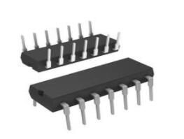
refers to the protective housing that encases an electronic component, providing mechanical support, electrical connections, and thermal management.
20-CDIP (0.300, 7.62mm) - Surface Mount
having leads that are designed to be soldered on the side of a circuit board that the body of the component is mounted on.
NO - Number of Pins20
- Usage LevelMilitary grade
- Operating Temperature
The operating temperature is the range of ambient temperature within which a power supply, or any other electrical equipment, operate in. This ranges from a minimum operating temperature, to a peak or maximum operating temperature, outside which, the power supply may fail.
-55°C~125°C - JESD-609 Code
The "JESD-609 Code" in electronic components refers to a standardized marking code that indicates the lead-free solder composition and finish of electronic components for compliance with environmental regulations.
e0 - Pbfree Code
The "Pbfree Code" parameter in electronic components refers to the code or marking used to indicate that the component is lead-free. Lead (Pb) is a toxic substance that has been widely used in electronic components for many years, but due to environmental concerns, there has been a shift towards lead-free alternatives. The Pbfree Code helps manufacturers and users easily identify components that do not contain lead, ensuring compliance with regulations and promoting environmentally friendly practices. It is important to pay attention to the Pbfree Code when selecting electronic components to ensure they meet the necessary requirements for lead-free applications.
no - Part Status
Parts can have many statuses as they progress through the configuration, analysis, review, and approval stages.
Active - Moisture Sensitivity Level (MSL)
Moisture Sensitivity Level (MSL) is a standardized rating that indicates the susceptibility of electronic components, particularly semiconductors, to moisture-induced damage during storage and the soldering process, defining the allowable exposure time to ambient conditions before they require special handling or baking to prevent failures
1 (Unlimited) - Number of Terminations20
- Terminal Finish
Terminal Finish refers to the surface treatment applied to the terminals or leads of electronic components to enhance their performance and longevity. It can improve solderability, corrosion resistance, and overall reliability of the connection in electronic assemblies. Common finishes include nickel, gold, and tin, each possessing distinct properties suitable for various applications. The choice of terminal finish can significantly impact the durability and effectiveness of electronic devices.
Tin/Lead (Sn/Pb) - Max Power Dissipation
The maximum power that the MOSFET can dissipate continuously under the specified thermal conditions.
30mW - Terminal Position
In electronic components, the term "Terminal Position" refers to the physical location of the connection points on the component where external electrical connections can be made. These connection points, known as terminals, are typically used to attach wires, leads, or other components to the main body of the electronic component. The terminal position is important for ensuring proper connectivity and functionality of the component within a circuit. It is often specified in technical datasheets or component specifications to help designers and engineers understand how to properly integrate the component into their circuit designs.
DUAL - Number of Functions2
- Supply Voltage
Supply voltage refers to the electrical potential difference provided to an electronic component or circuit. It is crucial for the proper operation of devices, as it powers their functions and determines performance characteristics. The supply voltage must be within specified limits to ensure reliability and prevent damage to components. Different electronic devices have specific supply voltage requirements, which can vary widely depending on their design and intended application.
5V - Base Part Number
The "Base Part Number" (BPN) in electronic components serves a similar purpose to the "Base Product Number." It refers to the primary identifier for a component that captures the essential characteristics shared by a group of similar components. The BPN provides a fundamental way to reference a family or series of components without specifying all the variations and specific details.
AD7528 - Pin Count
a count of all of the component leads (or pins)
20 - Qualification Status
An indicator of formal certification of qualifications.
Qualified - Output Type
The "Output Type" parameter in electronic components refers to the type of signal or data that is produced by the component as an output. This parameter specifies the nature of the output signal, such as analog or digital, and can also include details about the voltage levels, current levels, frequency, and other characteristics of the output signal. Understanding the output type of a component is crucial for ensuring compatibility with other components in a circuit or system, as well as for determining how the output signal can be utilized or processed further. In summary, the output type parameter provides essential information about the nature of the signal that is generated by the electronic component as its output.
Current - Unbuffered - Max Supply Voltage
In general, the absolute maximum common-mode voltage is VEE-0.3V and VCC+0.3V, but for products without a protection element at the VCC side, voltages up to the absolute maximum rated supply voltage (i.e. VEE+36V) can be supplied, regardless of supply voltage.
15V - Min Supply Voltage
The minimum supply voltage (V min ) is explored for sequential logic circuits by statistically simulating the impact of within-die process variations and gate-dielectric soft breakdown on data retention and hold time.
5V - Number of Bits8
- Architecture
In electronic components, the parameter "Architecture" refers to the overall design and structure of the component. It encompasses the arrangement of internal components, the layout of circuitry, and the physical form of the component. The architecture of an electronic component plays a crucial role in determining its functionality, performance, and compatibility with other components in a system. Different architectures can result in variations in power consumption, speed, size, and other key characteristics of the component. Designers often consider the architecture of electronic components carefully to ensure optimal performance and integration within a larger system.
R-2R - Converter Type
The parameter "Converter Type" in electronic components refers to the classification of devices that convert one form of energy or signal to another. This includes devices such as analog-to-digital converters (ADCs), digital-to-analog converters (DACs), and various types of signal converters used in communication, power management, and measurement systems. Each converter type is designed to facilitate the manipulation or transformation of signals to meet specific application requirements. The choice of converter type typically depends on factors such as the signal characteristics, required accuracy, and conversion speed.
D/A CONVERTER - Reference Type
a code object that is not stored directly where it is created, but that acts as a kind of pointer to a value stored elsewhere.
External - Data Interface
A Data Interface in EDQ is a template of a set of attributes representing a given entity, used to create processes that read from, or write to, interfaces rather than directly from or to sources or targets of data.
Parallel - Differential Output
a differential output voltage in electronics is the difference between the values of two AC voltages, 180° out of phase, present at the output terminals of an amplifier when you apply a differential input voltage to the input terminals of an amplifier.
No - Resolution
Resolution in electronic components refers to the smallest increment of measurement or change that can be detected or represented by the component. It is a crucial specification in devices such as sensors, displays, and converters, as it determines the level of detail or accuracy that can be achieved. For example, in a digital camera, resolution refers to the number of pixels that make up an image, with higher resolution indicating a greater level of detail. In analog-to-digital converters, resolution is the number of discrete values that can be represented in the digital output, determining the precision of the conversion process. Overall, resolution plays a significant role in determining the performance and capabilities of electronic components in various applications.
1 B - Sampling Rate
often described in the context of signal processing as the number of samples per time.
5.6 Msps - Voltage - Supply, Analog
Voltage - Supply, Analog is a parameter in electronic components that specifies the range of voltage levels required to power the analog circuitry within the component. This parameter indicates the minimum and maximum voltage levels that the component can accept for proper operation of its analog functions. It is crucial to ensure that the voltage supplied to the component falls within this specified range to prevent damage and ensure optimal performance. Understanding and adhering to the "Voltage - Supply, Analog" parameter is essential for the proper functioning of analog circuits in electronic components.
5V~15V - Voltage - Supply, Digital
Voltage - Supply, Digital is a parameter that specifies the voltage level required to power the digital circuitry within an electronic component, such as an integrated circuit or a microcontroller. This parameter is crucial for ensuring proper operation of the digital components, as supplying the correct voltage level is essential for reliable performance. The specified voltage range typically includes both minimum and maximum values within which the component can operate safely and efficiently. It is important to adhere to the recommended voltage supply range to prevent damage to the component and to maintain the integrity of the digital signals being processed.
5V~15V - Settling Time
In control theory the settling time of a dynamical system such as an amplifier or other output device is the time elapsed from the application of an ideal instantaneous step input to the time at which the amplifier output has entered and remained within a specified error band.
400ns - Integral Nonlinearity (INL)
Integral Nonlinearity (INL) is a measure of the deviation of a transfer function from a straight line when considering the entire output range of a device, such as a digital-to-analog converter or an analog-to-digital converter. It is quantified as the maximum deviation of the actual output from the ideal output across the entire input range, expressed as a percentage of the full-scale output. INL indicates how closely the output follows a linear model, influencing the accuracy of the signal representation in electronic components. A lower INL value signifies better linearity and higher precision in signal processing applications.
0.5 LSB - Input Bit Code
"Input Bit Code" is a parameter used in electronic components, particularly in digital devices such as microcontrollers and integrated circuits. It refers to the binary code or sequence of bits that are used to represent input data or commands to the component. The input bit code is typically specified by the manufacturer and is used to configure the behavior or functionality of the component.In simpler terms, the input bit code is like a set of instructions that the electronic component understands and acts upon accordingly. By providing the correct input bit code, users can control the operation of the component and make it perform specific tasks or functions. Understanding and correctly using the input bit code is essential for proper operation and integration of electronic components in various electronic systems and applications.
BINARY, OFFSET BINARY - Number of Converters2
- Conversion Rate
the number of conversions divided by the total number of visitors.
5.6 Msps - INL/DNL (LSB)
INL (Integral Non-Linearity) and DNL (Differential Non-Linearity) are parameters used to quantify the accuracy and performance of analog-to-digital converters (ADCs) and digital-to-analog converters (DACs). INL refers to the maximum deviation of the actual transfer function of a converter from a perfect straight line, representing the overall accuracy of the converter. DNL measures the difference between the actual step size of the output and the ideal step size, indicating the uniformity of the quantization levels. Both parameters are expressed in least significant bits (LSB), providing a standardized measure of the errors relative to the converter's resolution.
±0.5 (Max), ±1 (Max) - RoHS Status
RoHS means “Restriction of Certain Hazardous Substances” in the “Hazardous Substances Directive” in electrical and electronic equipment.
Non-RoHS Compliant - Lead Free
Lead Free is a term used to describe electronic components that do not contain lead as part of their composition. Lead is a toxic material that can have harmful effects on human health and the environment, so the electronics industry has been moving towards lead-free components to reduce these risks. Lead-free components are typically made using alternative materials such as silver, copper, and tin. Manufacturers must comply with regulations such as the Restriction of Hazardous Substances (RoHS) directive to ensure that their products are lead-free and environmentally friendly.
Contains Lead
Parts with Similar Specs
- ImagePart NumberManufacturerPackage / CaseNumber of PinsNumber of BitsSettling TimeIntegral Nonlinearity (INL)Min Supply VoltageSupply VoltageMax Supply VoltageView Compare
![5962-8770102RA]()
5962-8770102RA
20-CDIP (0.300, 7.62mm)
20
8
400ns
0.5 LSB
5 V
5 V
15 V
![AD7528CQ]()
20-CDIP (0.300, 7.62mm)
20
8
400ns
0.5 LSB
5 V
5 V
15 V
![AD7528BQ]()
20-CDIP (0.300, 7.62mm)
20
8
400ns
0.5 LSB
5 V
5 V
15 V
![AD7528TQ]()
20-CDIP (0.300, 7.62mm)
20
8
400ns
0.5 LSB
5 V
5 V
15 V

Datasheet PDF
- Datasheets :
- PCN Assembly/Origin :
- ConflictMineralStatement :
 2N5401 PNP Transistor: Pinout, Datasheet, and Equivalents
06 July 202128188
 STM32F446RET6 Microcontroller: 180MHz,64-LQFP, Pinout and Features
10 February 20226475
 LM319 Comparator: Datasheet, Pinout and Circuit
17 November 20214053
![LMR® -400 Coaxial Cables (RF) 50Ohms[Video]:Datasheet, Features, and Applications](https://res.utmel.com/Images/Article/fee4ddfa-7969-484f-ac95-2f6daa997670.png) LMR® -400 Coaxial Cables (RF) 50Ohms[Video]:Datasheet, Features, and Applications
LMR® -400 Coaxial Cables (RF) 50Ohms[Video]:Datasheet, Features, and Applications12 June 20245146
 LP2985 Low-Dropout Regulator: Pinout, Application and Package
19 July 20212608
 Designing with AD9850: Datasheet, Pinout, and Sine Wave Synthesis Guide
05 February 2026199
![OPA2134 VS TL072[Video]: What are the differences between them?](https://res.utmel.com/Images/Article/033d2d98-5d7e-40f2-9fc3-3620ad4995f8.png) OPA2134 VS TL072[Video]: What are the differences between them?
OPA2134 VS TL072[Video]: What are the differences between them?14 April 20229593
 43025-0800 Micro-Fit 3.0 Receptacle Housing Dual Row: Drawing, Datasheet, and Equivalents
11 February 20222530
 Utmel Discount Coupon is being delivered
19 October 20201616
 Car Sensors: Classification and Application
27 October 202513241
 What is Digital Signal Processing (DSP)?
17 March 20224863
 What is a Cascode Amplifier?
27 March 202515396
 ARM, FPGA, DSP and CPLD: Connection and Difference
15 March 20228369
 Verifying Package Pinout Compatibility: The Engineer's Guide to Component Replacement
06 June 202673
 Unveiling the Potential of GaN Semiconductor-Enabled Three-Phase Propulsion Inverters for Enhanced EV Performance
09 August 20231634
 Meta-Vision for CMOS Image Sensors: Beyond the Human Eye
15 March 20222764
Analog Devices Inc.
In Stock
United States
China
Canada
Japan
Russia
Germany
United Kingdom
Singapore
Italy
Hong Kong(China)
Taiwan(China)
France
Korea
Mexico
Netherlands
Malaysia
Austria
Spain
Switzerland
Poland
Thailand
Vietnam
India
United Arab Emirates
Afghanistan
Åland Islands
Albania
Algeria
American Samoa
Andorra
Angola
Anguilla
Antigua & Barbuda
Argentina
Armenia
Aruba
Australia
Azerbaijan
Bahamas
Bahrain
Bangladesh
Barbados
Belarus
Belgium
Belize
Benin
Bermuda
Bhutan
Bolivia
Bonaire, Sint Eustatius and Saba
Bosnia & Herzegovina
Botswana
Brazil
British Indian Ocean Territory
British Virgin Islands
Brunei
Bulgaria
Burkina Faso
Burundi
Cabo Verde
Cambodia
Cameroon
Cayman Islands
Central African Republic
Chad
Chile
Christmas Island
Cocos (Keeling) Islands
Colombia
Comoros
Congo
Congo (DRC)
Cook Islands
Costa Rica
Côte d’Ivoire
Croatia
Cuba
Curaçao
Cyprus
Czechia
Denmark
Djibouti
Dominica
Dominican Republic
Ecuador
Egypt
El Salvador
Equatorial Guinea
Eritrea
Estonia
Eswatini
Ethiopia
Falkland Islands
Faroe Islands
Fiji
Finland
French Guiana
French Polynesia
Gabon
Gambia
Georgia
Ghana
Gibraltar
Greece
Greenland
Grenada
Guadeloupe
Guam
Guatemala
Guernsey
Guinea
Guinea-Bissau
Guyana
Haiti
Honduras
Hungary
Iceland
Indonesia
Iran
Iraq
Ireland
Isle of Man
Israel
Jamaica
Jersey
Jordan
Kazakhstan
Kenya
Kiribati
Kosovo
Kuwait
Kyrgyzstan
Laos
Latvia
Lebanon
Lesotho
Liberia
Libya
Liechtenstein
Lithuania
Luxembourg
Macao(China)
Madagascar
Malawi
Maldives
Mali
Malta
Marshall Islands
Martinique
Mauritania
Mauritius
Mayotte
Micronesia
Moldova
Monaco
Mongolia
Montenegro
Montserrat
Morocco
Mozambique
Myanmar
Namibia
Nauru
Nepal
New Caledonia
New Zealand
Nicaragua
Niger
Nigeria
Niue
Norfolk Island
North Korea
North Macedonia
Northern Mariana Islands
Norway
Oman
Pakistan
Palau
Palestinian Authority
Panama
Papua New Guinea
Paraguay
Peru
Philippines
Pitcairn Islands
Portugal
Puerto Rico
Qatar
Réunion
Romania
Rwanda
Samoa
San Marino
São Tomé & Príncipe
Saudi Arabia
Senegal
Serbia
Seychelles
Sierra Leone
Sint Maarten
Slovakia
Slovenia
Solomon Islands
Somalia
South Africa
South Sudan
Sri Lanka
St Helena, Ascension, Tristan da Cunha
St. Barthélemy
St. Kitts & Nevis
St. Lucia
St. Martin
St. Pierre & Miquelon
St. Vincent & Grenadines
Sudan
Suriname
Svalbard & Jan Mayen
Sweden
Syria
Tajikistan
Tanzania
Timor-Leste
Togo
Tokelau
Tonga
Trinidad & Tobago
Tunisia
Turkey
Turkmenistan
Turks & Caicos Islands
Tuvalu
U.S. Outlying Islands
U.S. Virgin Islands
Uganda
Ukraine
Uruguay
Uzbekistan
Vanuatu
Vatican City
Venezuela
Wallis & Futuna
Yemen
Zambia
Zimbabwe
![AD5362BSTZ]() AD5362BSTZ
AD5362BSTZAnalog Devices Inc.
![AD7524LPZ]() AD7524LPZ
AD7524LPZAnalog Devices Inc.
![AD5420AREZ-REEL7]() AD5420AREZ-REEL7
AD5420AREZ-REEL7Analog Devices Inc.
![AD5328BRUZ-REEL7]() AD5328BRUZ-REEL7
AD5328BRUZ-REEL7Analog Devices Inc.
![ADV7125JSTZ330]() ADV7125JSTZ330
ADV7125JSTZ330Analog Devices Inc.
![AD5324ARMZ-REEL7]() AD5324ARMZ-REEL7
AD5324ARMZ-REEL7Analog Devices Inc.
![AD420ANZ-32]() AD420ANZ-32
AD420ANZ-32Analog Devices Inc.
![AD5304ARMZ]() AD5304ARMZ
AD5304ARMZAnalog Devices Inc.
![AD5683RBRMZ-3-RL7]() AD5683RBRMZ-3-RL7
AD5683RBRMZ-3-RL7Analog Devices Inc.
![AD5601BKSZ-REEL7]() AD5601BKSZ-REEL7
AD5601BKSZ-REEL7Analog Devices Inc.


