
 Product
 Brand
Brand Articles
 Tools
Tools
CD4503 Tri-state Hex Buffer: CD4503 Datasheet PDF, Pinout, CD4503 vs. MC14503


DUAL Buffers 16 Pins DIP
CD4503 is a hex non-inverting buffer with 3-state outputs having high sink- and source-current capability. This article will cover its datasheet, pinout, feature and more details about CD4503. Welcome your RFQ!
CD4503 Pinout

CD4503 Pinout
Pin No | Pin Name | Description |
1 | DIS A | Disable A |
2 | D1 | Input Pin Buffer 1 |
3 | Q1 | Output Pin Buffer 1 |
4 | D2 | Input Pin Buffer 2 |
5 | Q2 | Output Pin Buffer 2 |
6 | D3 | Input Pin Buffer 3 |
7 | Q3 | Output Pin Buffer 3 |
8 | VSS | Source Supply |
9 | Q4 | Output Pin Buffer 4 |
10 | D4 | Input Pin Buffer 4 |
11 | Q5 | Output Pin Buffer 5 |
12 | D5 | Input Pin Buffer 5 |
13 | Q6 | Output Pin Buffer 6 |
14 | D6 | Input Pin Buffer 6 |
15 | DIS B | Disable B |
16 | VDD | Drain supply |
CD4503 CAD Model
Symbol

CD4503 Symbol
Footprint

CD4503 Footprint
3D Model

CD4503 3D Model
CD4503 Descripton
CD4503 is a hex non-inverting buffer with three-state outputs that can handle a lot of sinks and source current. In 16-lead hermetic dual-in-line ceramic packaging, the CD4503 Hex buffer is available. This IC family offers a variety of functions, including ESD protection and thermal overload protection. In DLD design and logic switching applications, the Hex Buffer CD4503 is critical.
CD4503 Feature
■ Wide supply voltage range: 3.0 VDC to 18 VDC
■ 3-STATE outputs
■ Symmetrical turn on/turn off delays
■ Symmetrical output rise and fall times
■ Pin-for-pin replacement for MM80C97 and MC14503
CD4503 Application
3-State hex buffer for interfacing IC'S with data buses
CMOS to TTL Hex Buffer
Hex Buffers are also used to isolate other gates or circuit stages from each other preventing the impedance of one circuit from affecting the impedance of another
CD4503 Schematic
The following figure shows a schematic diagram of CD4503:

CD4503 Schematic Diagram
Specifications
- TypeParameter
- Mount
In electronic components, the term "Mount" typically refers to the method or process of physically attaching or fixing a component onto a circuit board or other electronic device. This can involve soldering, adhesive bonding, or other techniques to secure the component in place. The mounting process is crucial for ensuring proper electrical connections and mechanical stability within the electronic system. Different components may have specific mounting requirements based on their size, shape, and function, and manufacturers provide guidelines for proper mounting procedures to ensure optimal performance and reliability of the electronic device.
Through Hole - Package / Case
refers to the protective housing that encases an electronic component, providing mechanical support, electrical connections, and thermal management.
DIP - Number of Pins16
- Number of Elements2
- Number of Terminations16
- Max Operating Temperature
The Maximum Operating Temperature is the maximum body temperature at which the thermistor is designed to operate for extended periods of time with acceptable stability of its electrical characteristics.
125°C - Min Operating Temperature
The "Min Operating Temperature" parameter in electronic components refers to the lowest temperature at which the component is designed to operate effectively and reliably. This parameter is crucial for ensuring the proper functioning and longevity of the component, as operating below this temperature may lead to performance issues or even damage. Manufacturers specify the minimum operating temperature to provide guidance to users on the environmental conditions in which the component can safely operate. It is important to adhere to this parameter to prevent malfunctions and ensure the overall reliability of the electronic system.
-55°C - Additional Feature
Any Feature, including a modified Existing Feature, that is not an Existing Feature.
ONE FUNCTION WITH TWO BITS - Terminal Position
In electronic components, the term "Terminal Position" refers to the physical location of the connection points on the component where external electrical connections can be made. These connection points, known as terminals, are typically used to attach wires, leads, or other components to the main body of the electronic component. The terminal position is important for ensuring proper connectivity and functionality of the component within a circuit. It is often specified in technical datasheets or component specifications to help designers and engineers understand how to properly integrate the component into their circuit designs.
DUAL - Peak Reflow Temperature (Cel)
Peak Reflow Temperature (Cel) is a parameter that specifies the maximum temperature at which an electronic component can be exposed during the reflow soldering process. Reflow soldering is a common method used to attach electronic components to a circuit board. The Peak Reflow Temperature is crucial because it ensures that the component is not damaged or degraded during the soldering process. Exceeding the specified Peak Reflow Temperature can lead to issues such as component failure, reduced performance, or even permanent damage to the component. It is important for manufacturers and assemblers to adhere to the recommended Peak Reflow Temperature to ensure the reliability and functionality of the electronic components.
NOT SPECIFIED - Number of Functions2
- Supply Voltage
Supply voltage refers to the electrical potential difference provided to an electronic component or circuit. It is crucial for the proper operation of devices, as it powers their functions and determines performance characteristics. The supply voltage must be within specified limits to ensure reliability and prevent damage to components. Different electronic devices have specific supply voltage requirements, which can vary widely depending on their design and intended application.
5V - Reach Compliance Code
Reach Compliance Code refers to a designation indicating that electronic components meet the requirements set by the Registration, Evaluation, Authorization, and Restriction of Chemicals (REACH) regulation in the European Union. It signifies that the manufacturer has assessed and managed the chemical substances within the components to ensure safety and environmental protection. This code is vital for compliance with regulations aimed at minimizing risks associated with hazardous substances in electronic products.
unknown - Time@Peak Reflow Temperature-Max (s)
Time@Peak Reflow Temperature-Max (s) refers to the maximum duration that an electronic component can be exposed to the peak reflow temperature during the soldering process, which is crucial for ensuring reliable solder joint formation without damaging the component.
NOT SPECIFIED - Pin Count
a count of all of the component leads (or pins)
16 - Qualification Status
An indicator of formal certification of qualifications.
Not Qualified - Polarity
In electronic components, polarity refers to the orientation or direction in which the component must be connected in a circuit to function properly. Components such as diodes, capacitors, and LEDs have polarity markings to indicate which terminal should be connected to the positive or negative side of the circuit. Connecting a component with incorrect polarity can lead to malfunction or damage. It is important to pay attention to polarity markings and follow the manufacturer's instructions to ensure proper operation of electronic components.
Non-Inverting - Temperature Grade
Temperature grades represent a tire's resistance to heat and its ability to dissipate heat when tested under controlled laboratory test conditions.
MILITARY - Number of Channels6
- Max Supply Voltage
In general, the absolute maximum common-mode voltage is VEE-0.3V and VCC+0.3V, but for products without a protection element at the VCC side, voltages up to the absolute maximum rated supply voltage (i.e. VEE+36V) can be supplied, regardless of supply voltage.
15V - Min Supply Voltage
The minimum supply voltage (V min ) is explored for sequential logic circuits by statistically simulating the impact of within-die process variations and gate-dielectric soft breakdown on data retention and hold time.
3V - Load Capacitance
the amount of capacitance measured or computed across the crystal terminals on the PCB. Frequency Tolerance. Frequency tolerance refers to the allowable deviation from nominal, in parts per million (PPM), at a specific temperature, usually +25°C.
50pF - Number of Ports
A port is identified for each transport protocol and address combination by a 16-bit unsigned number,.
2 - Number of Bits4
- Propagation Delay
the flight time of packets over the transmission link and is limited by the speed of light.
30 ns - Quiescent Current
The quiescent current is defined as the current level in the amplifier when it is producing an output of zero.
4μA - Turn On Delay Time
Turn-on delay, td(on), is the time taken to charge the input capacitance of the device before drain current conduction can start.
175 ns - Family
In electronic components, the parameter "Family" typically refers to a categorization or classification system used to group similar components together based on their characteristics, functions, or applications. This classification helps users easily identify and select components that meet their specific requirements. The "Family" parameter can include various subcategories such as resistors, capacitors, diodes, transistors, integrated circuits, and more. Understanding the "Family" of an electronic component can provide valuable information about its compatibility, performance specifications, and potential uses within a circuit or system. It is important to consider the "Family" parameter when designing or troubleshooting electronic circuits to ensure proper functionality and compatibility with other components.
4000/14000/40000 - Logic Function
In electronic components, the term "Logic Function" refers to the specific operation or behavior of a component based on its input signals. It describes how the component processes the input signals to produce the desired output. Logic functions are fundamental to digital circuits and are used to perform logical operations such as AND, OR, NOT, and XOR.Each electronic component, such as logic gates or flip-flops, is designed to perform a specific logic function based on its internal circuitry. By understanding the logic function of a component, engineers can design and analyze complex digital systems to ensure proper functionality and performance. Different logic functions can be combined to create more complex operations, allowing for the creation of sophisticated digital devices and systems.
Buffer, Inverting - Output Characteristics
Output characteristics in electronic components refer to the relationship between the output voltage and output current across a range of input conditions. This parameter is essential for understanding how a device, such as a transistor or operational amplifier, behaves under various loads and operating points. It provides insights into the efficiency, performance, and limitations of the component, helping designers to make informed choices for circuits and applications.
3-STATE - Logic IC Type
Logic IC Type refers to the type of integrated circuit (IC) that is specifically designed to perform logical operations. These ICs are commonly used in digital electronic devices to process and manipulate binary data according to predefined logic functions. The Logic IC Type parameter typically specifies the specific logic family or technology used in the IC, such as TTL (Transistor-Transistor Logic), CMOS (Complementary Metal-Oxide-Semiconductor), or ECL (Emitter-Coupled Logic). Understanding the Logic IC Type is important for selecting the appropriate IC for a given application, as different logic families have varying characteristics in terms of speed, power consumption, and noise immunity.
BUS DRIVER - Prop. Delay@Nom-Sup
The parameter "Prop. Delay@Nom-Sup" in electronic components refers to the propagation delay at nominal supply voltage. Propagation delay is the time it takes for a signal to travel from the input of a component to the output, typically measured in nanoseconds or picoseconds. The nominal supply voltage is the standard operating voltage specified for the component.This parameter is important because it affects the overall speed and performance of the electronic circuit. A shorter propagation delay means faster signal processing and better overall performance. Designers need to consider the propagation delay at the nominal supply voltage when selecting components for their circuits to ensure proper functionality and meet performance requirements.
100 ns - High Level Output Current
High-level Output Current IOH The current flowing into the output at a specified high- level voltage. Low-level Output Current IOL The current flowing into the output at a specified low- level output voltage.
-8.2mA - Low Level Output Current
The current into the output terminal with input conditions applied that, according to the product specification, will establish a low level at the output.
19.95mA - Control Type
Control Type in electronic components refers to the method used to regulate or manipulate an electronic system's behavior or output. It can indicate whether the component operates in an analog or digital manner, and may include types such as on/off, proportional, or pulse-width modulation. Understanding the control type is crucial for determining how components interact with each other and the overall system's functionality.
ENABLE LOW - Length19.305mm
- Height Seated (Max)
Height Seated (Max) is a parameter in electronic components that refers to the maximum allowable height of the component when it is properly seated or installed on a circuit board or within an enclosure. This specification is crucial for ensuring proper fit and alignment within the overall system design. Exceeding the maximum seated height can lead to mechanical interference, electrical shorts, or other issues that may impact the performance and reliability of the electronic device. Manufacturers provide this information to help designers and engineers select components that will fit within the designated space and function correctly in the intended application.
5.08mm - RoHS Status
RoHS means “Restriction of Certain Hazardous Substances” in the “Hazardous Substances Directive” in electrical and electronic equipment.
RoHS Compliant - Lead Free
Lead Free is a term used to describe electronic components that do not contain lead as part of their composition. Lead is a toxic material that can have harmful effects on human health and the environment, so the electronics industry has been moving towards lead-free components to reduce these risks. Lead-free components are typically made using alternative materials such as silver, copper, and tin. Manufacturers must comply with regulations such as the Restriction of Hazardous Substances (RoHS) directive to ensure that their products are lead-free and environmentally friendly.
Lead Free
Parts with Similar Specs
CD4503 Physical Dimensions

CD4503 Physical Dimensions
CD4503 Manufacturer
ON Semiconductor has completed its acquisition of Fairchild. Together, we deliver a more extensive product portfolio of power discretes, ICs and power modules, plus a complete offering of low, mid and high voltage products across the entire voltage spectrum which means more choices for your designs. Together, we provide a stronger presence in the key markets of automotive, industrial and wireless, combined with increased technical and sales support.
Datasheet PDF
- Datasheets :
- ReachStatement :
Trend Analysis
What is A Hex Buffer?
A buffer is a simple logic gate that sends its input to its output unmodified. It behaves in the opposite way that a NOT gate does. The primary function of a buffer is to regenerate the input signal, which is commonly accomplished by utilizing a strong high and a strong low. A buffer has only one input and output, and its output is always the same as its input. Buffers are also utilized to drive huge capacitive loads, which increases the propagation delay of circuits.
What is a hex buffer used for?
These hex buffers and drivers feature high-voltage open-collector outputs to interface with high-level circuits or for driving high-current loads. They are also characterized for use as buffers for driving TTL inputs.
What is the difference between buffer and inverter?
An inverter is a logic gate whose output (X) is the inverse of its input (A). A buffer is a type of logic gate that is used to increase drive capability in order to increase the number of fanouts or the signal speed. A buffer does not perform any logical operation. It also helps shape the waveform of a signal.
 AO4466 30V N-Channel MOSFET, 10A 8SOIC, AO4466 Datasheet pdf
11 February 20224782
![How to Use BC547B Transistor as a Switch or an Amplifier?[ Video]](https://res.utmel.com/Images/Article/334c4527-7050-48e2-a137-ec8df881fc76.jpg) How to Use BC547B Transistor as a Switch or an Amplifier?[ Video]
How to Use BC547B Transistor as a Switch or an Amplifier?[ Video]07 April 20223648
 TXS0104ERGYR: 4-Bit Bidirectional Voltage-Level Translator, Datasheet
22 March 20221905
 SFH620A Optocoupler: Datasheet, Pinout, Circuit
09 March 20222226
 The General Introduction to 1N747
28 April 20221144
 P82B96 Bipolar IC: Pinout, 3D Model and Datasheet
02 November 20212838
 AP7331 Linear Regulator: Features, Pinout and Datasheet
11 March 2022966
 TDA7850 Amplifier: Package, Pinout, and Datasheet
27 October 202114321
 How Many do You Know About the 12 Components Included in the Circuit Board?
12 February 20228796
 FPGA vs SoC: A Comprehensive Comparison Guide
13 May 20255244
 What is PWM "Dead Band"?
21 April 20227783
 The Difference and Application of SPI, UART, I2C Communication
15 October 202511818
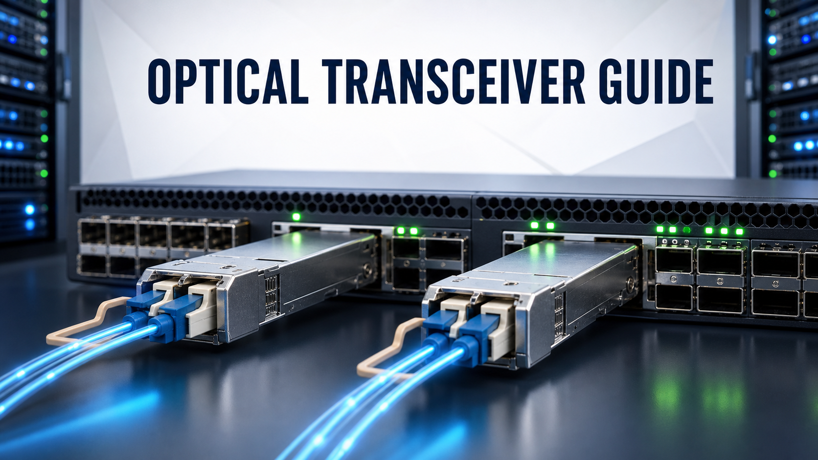 Optical Transceiver Guide: How It Works, Types, Form Factors, and Selection
24 June 2026145
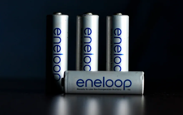 SR44 vs LR44 Which Battery Should You Use
21 August 20252593
 Does the Terminal Resistance of the CAN Bus Have to be 120Ω?
19 April 202236709
 An Overview of LPDDR
25 March 202636818
Fairchild (ON Semiconductor)
In Stock: 159
United States
China
Canada
Japan
Russia
Germany
United Kingdom
Singapore
Italy
Hong Kong(China)
Taiwan(China)
France
Korea
Mexico
Netherlands
Malaysia
Austria
Spain
Switzerland
Poland
Thailand
Vietnam
India
United Arab Emirates
Afghanistan
Åland Islands
Albania
Algeria
American Samoa
Andorra
Angola
Anguilla
Antigua & Barbuda
Argentina
Armenia
Aruba
Australia
Azerbaijan
Bahamas
Bahrain
Bangladesh
Barbados
Belarus
Belgium
Belize
Benin
Bermuda
Bhutan
Bolivia
Bonaire, Sint Eustatius and Saba
Bosnia & Herzegovina
Botswana
Brazil
British Indian Ocean Territory
British Virgin Islands
Brunei
Bulgaria
Burkina Faso
Burundi
Cabo Verde
Cambodia
Cameroon
Cayman Islands
Central African Republic
Chad
Chile
Christmas Island
Cocos (Keeling) Islands
Colombia
Comoros
Congo
Congo (DRC)
Cook Islands
Costa Rica
Côte d’Ivoire
Croatia
Cuba
Curaçao
Cyprus
Czechia
Denmark
Djibouti
Dominica
Dominican Republic
Ecuador
Egypt
El Salvador
Equatorial Guinea
Eritrea
Estonia
Eswatini
Ethiopia
Falkland Islands
Faroe Islands
Fiji
Finland
French Guiana
French Polynesia
Gabon
Gambia
Georgia
Ghana
Gibraltar
Greece
Greenland
Grenada
Guadeloupe
Guam
Guatemala
Guernsey
Guinea
Guinea-Bissau
Guyana
Haiti
Honduras
Hungary
Iceland
Indonesia
Iran
Iraq
Ireland
Isle of Man
Israel
Jamaica
Jersey
Jordan
Kazakhstan
Kenya
Kiribati
Kosovo
Kuwait
Kyrgyzstan
Laos
Latvia
Lebanon
Lesotho
Liberia
Libya
Liechtenstein
Lithuania
Luxembourg
Macao(China)
Madagascar
Malawi
Maldives
Mali
Malta
Marshall Islands
Martinique
Mauritania
Mauritius
Mayotte
Micronesia
Moldova
Monaco
Mongolia
Montenegro
Montserrat
Morocco
Mozambique
Myanmar
Namibia
Nauru
Nepal
New Caledonia
New Zealand
Nicaragua
Niger
Nigeria
Niue
Norfolk Island
North Korea
North Macedonia
Northern Mariana Islands
Norway
Oman
Pakistan
Palau
Palestinian Authority
Panama
Papua New Guinea
Paraguay
Peru
Philippines
Pitcairn Islands
Portugal
Puerto Rico
Qatar
Réunion
Romania
Rwanda
Samoa
San Marino
São Tomé & Príncipe
Saudi Arabia
Senegal
Serbia
Seychelles
Sierra Leone
Sint Maarten
Slovakia
Slovenia
Solomon Islands
Somalia
South Africa
South Sudan
Sri Lanka
St Helena, Ascension, Tristan da Cunha
St. Barthélemy
St. Kitts & Nevis
St. Lucia
St. Martin
St. Pierre & Miquelon
St. Vincent & Grenadines
Sudan
Suriname
Svalbard & Jan Mayen
Sweden
Syria
Tajikistan
Tanzania
Timor-Leste
Togo
Tokelau
Tonga
Trinidad & Tobago
Tunisia
Turkey
Turkmenistan
Turks & Caicos Islands
Tuvalu
U.S. Outlying Islands
U.S. Virgin Islands
Uganda
Ukraine
Uruguay
Uzbekistan
Vanuatu
Vatican City
Venezuela
Wallis & Futuna
Yemen
Zambia
Zimbabwe
![NC7SZ126L6X]() NC7SZ126L6X
NC7SZ126L6XFairchild
![74LCX543MSA]() 74LCX543MSA
74LCX543MSAFairchild
![74LCX245SJX]() 74LCX245SJX
74LCX245SJXFairchild
![74LVQ244SCX]() 74LVQ244SCX
74LVQ244SCXFairchild
![74LCX16245GX]() 74LCX16245GX
74LCX16245GXFairchild
![74LVQ125SC]() 74LVQ125SC
74LVQ125SCFairchild
![74LVT16240MTDX]() 74LVT16240MTDX
74LVT16240MTDXFairchild
![74LVTH543WMX]() 74LVTH543WMX
74LVTH543WMXFairchild
![74LCX543MTCX]() 74LCX543MTCX
74LCX543MTCXFairchild
![74LCX240MTC]() 74LCX240MTC
74LCX240MTCFairchild
