
 Product
 Brand
Brand Articles
 Tools
Tools
S8050 NPN Silicon Transistors: Datasheet, Pinout and Equivalent


TRANSISTOR TO-92
S8050 is an NPN, a general-purpose transistor. This article mainly covers datasheet, pinout, equivalents, applications, and other details about S8050.

How to make Audio amplifier using s8050 Transistor
S8050 Pinout

S8050 Pinout
| Pin Number | Pin Name | Description |
| 1 | Emitter | Current Drains out through emitter |
| 2 | Base | Controls the biasing of transistor |
| 3 | Collector | Current flows in through collector |
S8050 Description
S8050 is a general-purpose transistor, which is a perfect transistor to perform small and general tasks in electronic circuits. S8050 is an NPN transistor hence the collector and emitter will be left open (Reverse biased) when the base pin is held at the ground and will be closed (Forward biased) when a signal is provided to the base pin. It has a maximum gain value of 400; this value determines the amplification capacity of the transistor normally S8050.
You can use it as a switch in electronic circuits to switch on loads under 700mA. 700mA is enough to handle a variety of loads for example relays, LEDs, bulbs, etc.
S8050 Features
Low Voltage, High Current NPN Transistor
Small Signal Transistor
Maximum Power: 2 Watts
Maximum DC Current Gain (hFE) is 400
Continuous Collector current (IC) is 700mA
Base- Emitter Voltage (VBE) is 5V
Collector-Emitter Voltage (VCE) is 20V
Collector-Base Voltage (VCB) is 30V
High Used in push-pull configuration doe Class B amplifiers
Available in To-92 Package
Specifications
- TypeParameter
- Mounting Type
The "Mounting Type" in electronic components refers to the method used to attach or connect a component to a circuit board or other substrate, such as through-hole, surface-mount, or panel mount.
Through Hole - Package / Case
refers to the protective housing that encases an electronic component, providing mechanical support, electrical connections, and thermal management.
TO-226-3, TO-92-3 (TO-226AA) Formed Leads - Surface Mount
having leads that are designed to be soldered on the side of a circuit board that the body of the component is mounted on.
NO - Transistor Element Material
The "Transistor Element Material" parameter in electronic components refers to the material used to construct the transistor within the component. Transistors are semiconductor devices that amplify or switch electronic signals and are a fundamental building block in electronic circuits. The material used for the transistor element can significantly impact the performance and characteristics of the component. Common materials used for transistor elements include silicon, germanium, and gallium arsenide, each with its own unique properties and suitability for different applications. The choice of transistor element material is crucial in designing electronic components to meet specific performance requirements such as speed, power efficiency, and temperature tolerance.
SILICON - Current-Collector (Ic) (Max)500mA
- Number of Elements1
- Operating Temperature
The operating temperature is the range of ambient temperature within which a power supply, or any other electrical equipment, operate in. This ranges from a minimum operating temperature, to a peak or maximum operating temperature, outside which, the power supply may fail.
-55°C~150°C TJ - Published2007
- JESD-609 Code
The "JESD-609 Code" in electronic components refers to a standardized marking code that indicates the lead-free solder composition and finish of electronic components for compliance with environmental regulations.
e3 - Pbfree Code
The "Pbfree Code" parameter in electronic components refers to the code or marking used to indicate that the component is lead-free. Lead (Pb) is a toxic substance that has been widely used in electronic components for many years, but due to environmental concerns, there has been a shift towards lead-free alternatives. The Pbfree Code helps manufacturers and users easily identify components that do not contain lead, ensuring compliance with regulations and promoting environmentally friendly practices. It is important to pay attention to the Pbfree Code when selecting electronic components to ensure they meet the necessary requirements for lead-free applications.
yes - Part Status
Parts can have many statuses as they progress through the configuration, analysis, review, and approval stages.
Last Time Buy - Moisture Sensitivity Level (MSL)
Moisture Sensitivity Level (MSL) is a standardized rating that indicates the susceptibility of electronic components, particularly semiconductors, to moisture-induced damage during storage and the soldering process, defining the allowable exposure time to ambient conditions before they require special handling or baking to prevent failures
1 (Unlimited) - Number of Terminations3
- ECCN Code
An ECCN (Export Control Classification Number) is an alphanumeric code used by the U.S. Bureau of Industry and Security to identify and categorize electronic components and other dual-use items that may require an export license based on their technical characteristics and potential for military use.
EAR99 - Terminal Finish
Terminal Finish refers to the surface treatment applied to the terminals or leads of electronic components to enhance their performance and longevity. It can improve solderability, corrosion resistance, and overall reliability of the connection in electronic assemblies. Common finishes include nickel, gold, and tin, each possessing distinct properties suitable for various applications. The choice of terminal finish can significantly impact the durability and effectiveness of electronic devices.
Matte Tin (Sn) - Terminal Position
In electronic components, the term "Terminal Position" refers to the physical location of the connection points on the component where external electrical connections can be made. These connection points, known as terminals, are typically used to attach wires, leads, or other components to the main body of the electronic component. The terminal position is important for ensuring proper connectivity and functionality of the component within a circuit. It is often specified in technical datasheets or component specifications to help designers and engineers understand how to properly integrate the component into their circuit designs.
BOTTOM - Peak Reflow Temperature (Cel)
Peak Reflow Temperature (Cel) is a parameter that specifies the maximum temperature at which an electronic component can be exposed during the reflow soldering process. Reflow soldering is a common method used to attach electronic components to a circuit board. The Peak Reflow Temperature is crucial because it ensures that the component is not damaged or degraded during the soldering process. Exceeding the specified Peak Reflow Temperature can lead to issues such as component failure, reduced performance, or even permanent damage to the component. It is important for manufacturers and assemblers to adhere to the recommended Peak Reflow Temperature to ensure the reliability and functionality of the electronic components.
NOT SPECIFIED - Time@Peak Reflow Temperature-Max (s)
Time@Peak Reflow Temperature-Max (s) refers to the maximum duration that an electronic component can be exposed to the peak reflow temperature during the soldering process, which is crucial for ensuring reliable solder joint formation without damaging the component.
NOT SPECIFIED - Pin Count
a count of all of the component leads (or pins)
3 - JESD-30 Code
JESD-30 Code refers to a standardized descriptive designation system established by JEDEC for semiconductor-device packages. This system provides a systematic method for generating designators that convey essential information about the package's physical characteristics, such as size and shape, which aids in component identification and selection. By using JESD-30 codes, manufacturers and engineers can ensure consistency and clarity in the specification of semiconductor packages across various applications and industries.
O-PBCY-T3 - Qualification Status
An indicator of formal certification of qualifications.
Not Qualified - Configuration
The parameter "Configuration" in electronic components refers to the specific arrangement or setup of the components within a circuit or system. It encompasses how individual elements are interconnected and their physical layout. Configuration can affect the functionality, performance, and efficiency of the electronic system, and may influence factors such as signal flow, impedance, and power distribution. Understanding the configuration is essential for design, troubleshooting, and optimizing electronic devices.
SINGLE - Power - Max
Power - Max is a parameter that specifies the maximum amount of power that an electronic component can handle without being damaged. It is typically measured in watts and indicates the upper limit of power that can be safely supplied to the component. Exceeding the maximum power rating can lead to overheating, malfunction, or permanent damage to the component. It is important to consider the power-max rating when designing circuits or systems to ensure proper operation and longevity of the electronic components.
625MW - Polarity/Channel Type
In electronic components, the parameter "Polarity/Channel Type" refers to the characteristic that determines the direction of current flow or the type of signal that can be accommodated by the component. For components like diodes and transistors, polarity indicates the direction in which current can flow through the component, such as forward bias or reverse bias for diodes. For components like MOSFETs or JFETs, the channel type refers to whether the component is an N-channel or P-channel device, which determines the type of charge carriers that carry current through the component. Understanding the polarity or channel type of a component is crucial for proper circuit design and ensuring that the component is connected correctly to achieve the desired functionality.
NPN - Transistor Type
Transistor type refers to the classification of transistors based on their operation and construction. The two primary types are bipolar junction transistors (BJTs) and field-effect transistors (FETs). BJTs use current to control the flow of current, while FETs utilize voltage to control current flow. Each type has its own subtypes, such as NPN and PNP for BJTs, and MOSFETs and JFETs for FETs, impacting their applications and characteristics in electronic circuits.
NPN - DC Current Gain (hFE) (Min) @ Ic, Vce
The parameter "DC Current Gain (hFE) (Min) @ Ic, Vce" in electronic components refers to the minimum value of the DC current gain, denoted as hFE, under specific operating conditions of collector current (Ic) and collector-emitter voltage (Vce). The DC current gain hFE represents the ratio of the collector current to the base current in a bipolar junction transistor (BJT), indicating the amplification capability of the transistor. The minimum hFE value at a given Ic and Vce helps determine the transistor's performance and efficiency in amplifying signals within a circuit. Designers use this parameter to ensure proper transistor selection and performance in various electronic applications.
160 @ 50mA 1V - Current - Collector Cutoff (Max)
The parameter "Current - Collector Cutoff (Max)" refers to the maximum current at which a transistor or other electronic component will cease to conduct current between the collector and emitter terminals. This parameter is important in determining the maximum current that can flow through the component when it is in the cutoff state. Exceeding this maximum cutoff current can lead to malfunction or damage of the component. It is typically specified in the component's datasheet and is crucial for proper circuit design and operation.
100nA - Vce Saturation (Max) @ Ib, Ic
The parameter "Vce Saturation (Max) @ Ib, Ic" in electronic components refers to the maximum voltage drop across the collector-emitter junction when the transistor is in saturation mode. This parameter is specified at a certain base current (Ib) and collector current (Ic) levels. It indicates the minimum voltage required to keep the transistor fully conducting in saturation mode, ensuring that the transistor operates efficiently and does not enter the cutoff region. Designers use this parameter to ensure proper transistor operation and to prevent overheating or damage to the component.
600mV @ 50mA, 500mA - Voltage - Collector Emitter Breakdown (Max)
Voltage - Collector Emitter Breakdown (Max) is a parameter that specifies the maximum voltage that can be applied between the collector and emitter terminals of a transistor or other semiconductor device before it breaks down and allows excessive current to flow. This parameter is crucial for ensuring the safe and reliable operation of the component within its specified limits. Exceeding the maximum breakdown voltage can lead to permanent damage or failure of the device. Designers and engineers must carefully consider this parameter when selecting components for their circuits to prevent potential issues and ensure proper functionality.
25V - Transition Frequency
Transition Frequency in electronic components refers to the frequency at which a device can transition from one state to another, typically defining the upper limit of its operating frequency. It is a critical parameter in determining the speed and performance of active components like transistors and integrated circuits. This frequency is influenced by factors such as capacitance, resistance, and the inherent characteristics of the materials used in the component's construction. Understanding transition frequency is essential for optimizing circuit designs and ensuring reliable signal processing in various applications.
150MHz - Frequency - Transition
The parameter "Frequency - Transition" in electronic components refers to the maximum frequency at which a signal transition can occur within the component. It is a crucial specification for digital circuits as it determines the speed at which data can be processed and transmitted. A higher frequency transition allows for faster operation and better performance of the electronic component. It is typically measured in hertz (Hz) or megahertz (MHz) and is specified by the manufacturer to ensure proper functioning of the component within a given frequency range.
150MHz - RoHS Status
RoHS means “Restriction of Certain Hazardous Substances” in the “Hazardous Substances Directive” in electrical and electronic equipment.
ROHS3 Compliant
S8050 Applications
Audio amplification circuits
Class B amplifiers
Push-pull transistors
Circuits where high gain is required
Low signal applications
S8050 Circuit

S8050 Circuit
Where to use S8050
S8050 transistor is a general-purpose transistor that is also a perfect transistor to perform small and general tasks in electronic circuits. You can use it as a switch in electronic circuits to switch on loads under 700mA. 700mA is enough to handle a variety of loads for example relays, LEDs, bulbs, etc.
S8050 Equivalents
2N5830, S9013
S8050 vs. 2N2222
2N2222 is a low-power NPN transistor. The current expansion is full 250MHZ; the magnification is 100-300; the withstand voltage is 40v; the current is 0.6a, and the power is 0.625w.
As for S8050 NPN, the maximum collecting current is 0.7A, power consumption is 625 mW; the maximum collecting coating-pole voltage is 25v, and the characteristic frequency is 150 MH
S8050 Package


S8050 Manufacturer
MCC produces high-quality discrete semiconductors to the consumer and industrial markets—including diodes, rectifiers, MOSFETs, voltage regulators, and protection devices.
Datasheet PDF
- PCN Obsolescence/ EOL :
- Datasheets :
What type of transistor is S8050?
S8050 transistor is a general-purpose transistor and it is a perfect transistor to perform small and general tasks in electronic circuits. You can use it as a switch in electronic circuits to switch on loads under 700mA.
Is S8050 transistor NPN or PNP?
S8050 is an NPN transistor hence the collector and emitter will be left open (Reverse biased) when the base pin is held at the ground and will be closed (Forward biased) when a signal is provided to the base pin.
How does S8050 work?
S8050 is an NPN transistor hence the collector and emitter will be left open (Reverse biased) when the base pin is held at the ground and will be closed (Forward biased) when a signal is provided to the base pin. When this transistor is fully biassed then it can allow a maximum of 700mA to flow across the collector and emitter.
What is the maximum gain value of S8050?
700mA
What can S8050 transistor be used to switch on loads under 700mA?
switch in electronic circuits
What is the operating temperature of s8050 transistor?
-55°C~150°C TJ
![2SD313 NPN Power Transistor: 2SD313 Datasheet pdf, Pinout and Replacements [Video]](https://res.utmel.com/Images/Article/2debbf0b-1ff1-4fee-bd2a-e735bf39907d.jpg) 2SD313 NPN Power Transistor: 2SD313 Datasheet pdf, Pinout and Replacements [Video]
2SD313 NPN Power Transistor: 2SD313 Datasheet pdf, Pinout and Replacements [Video]21 April 20255879
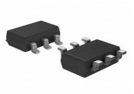 AOZ1280CI 1.2 A Simple Buck Regulator, SOT-23-6 1.5 MHz EZ Buck
12 February 20224308
 RFP30N06LE Power MOSFET: Equivalent, Circuit, and Datasheet
12 August 20215710
 UA741CP Operational Amplifier: Pinout, Specification, and Datasheet
18 June 202118285
 1N914 Diode: Alternatives, Features and Datasheet
09 August 20218716
 A Comprehensive Guide to LTC6995CS6-2#TRPBF Programmable Timer and Oscillator
06 March 2024324
 TMS320F28069PZT: Unraveling the 32-bit ControlCARD Microcontroller by Texas Instruments
29 February 2024155
 A Comprehensive Guide to LTC6900CS5#TRMPBF Programmable Timer and Oscillator
06 March 2024703
 What is a Transmitter?
12 October 20215702
 What are Electromagnetic Waves?
07 December 20215425
 Wireless Charging Explained: Working and Standards
26 May 202110461
 What is a Transformer: Definition, Principle and Applications
03 November 20218150
 Semiconductor Devices: Impact on IoT and Modern Communication (Part- 2)
24 July 20242892
 What is the DC Bias Characteristic of a Capacitor?
25 July 202211705
 What is a High-pass Filter?
10 March 202114447
 Methods for measuring the temperature of semiconductor devices
14 November 20222264
Micro Commercial Co
In Stock
United States
China
Canada
Japan
Russia
Germany
United Kingdom
Singapore
Italy
Hong Kong(China)
Taiwan(China)
France
Korea
Mexico
Netherlands
Malaysia
Austria
Spain
Switzerland
Poland
Thailand
Vietnam
India
United Arab Emirates
Afghanistan
Åland Islands
Albania
Algeria
American Samoa
Andorra
Angola
Anguilla
Antigua & Barbuda
Argentina
Armenia
Aruba
Australia
Azerbaijan
Bahamas
Bahrain
Bangladesh
Barbados
Belarus
Belgium
Belize
Benin
Bermuda
Bhutan
Bolivia
Bonaire, Sint Eustatius and Saba
Bosnia & Herzegovina
Botswana
Brazil
British Indian Ocean Territory
British Virgin Islands
Brunei
Bulgaria
Burkina Faso
Burundi
Cabo Verde
Cambodia
Cameroon
Cayman Islands
Central African Republic
Chad
Chile
Christmas Island
Cocos (Keeling) Islands
Colombia
Comoros
Congo
Congo (DRC)
Cook Islands
Costa Rica
Côte d’Ivoire
Croatia
Cuba
Curaçao
Cyprus
Czechia
Denmark
Djibouti
Dominica
Dominican Republic
Ecuador
Egypt
El Salvador
Equatorial Guinea
Eritrea
Estonia
Eswatini
Ethiopia
Falkland Islands
Faroe Islands
Fiji
Finland
French Guiana
French Polynesia
Gabon
Gambia
Georgia
Ghana
Gibraltar
Greece
Greenland
Grenada
Guadeloupe
Guam
Guatemala
Guernsey
Guinea
Guinea-Bissau
Guyana
Haiti
Honduras
Hungary
Iceland
Indonesia
Iran
Iraq
Ireland
Isle of Man
Israel
Jamaica
Jersey
Jordan
Kazakhstan
Kenya
Kiribati
Kosovo
Kuwait
Kyrgyzstan
Laos
Latvia
Lebanon
Lesotho
Liberia
Libya
Liechtenstein
Lithuania
Luxembourg
Macao(China)
Madagascar
Malawi
Maldives
Mali
Malta
Marshall Islands
Martinique
Mauritania
Mauritius
Mayotte
Micronesia
Moldova
Monaco
Mongolia
Montenegro
Montserrat
Morocco
Mozambique
Myanmar
Namibia
Nauru
Nepal
New Caledonia
New Zealand
Nicaragua
Niger
Nigeria
Niue
Norfolk Island
North Korea
North Macedonia
Northern Mariana Islands
Norway
Oman
Pakistan
Palau
Palestinian Authority
Panama
Papua New Guinea
Paraguay
Peru
Philippines
Pitcairn Islands
Portugal
Puerto Rico
Qatar
Réunion
Romania
Rwanda
Samoa
San Marino
São Tomé & Príncipe
Saudi Arabia
Senegal
Serbia
Seychelles
Sierra Leone
Sint Maarten
Slovakia
Slovenia
Solomon Islands
Somalia
South Africa
South Sudan
Sri Lanka
St Helena, Ascension, Tristan da Cunha
St. Barthélemy
St. Kitts & Nevis
St. Lucia
St. Martin
St. Pierre & Miquelon
St. Vincent & Grenadines
Sudan
Suriname
Svalbard & Jan Mayen
Sweden
Syria
Tajikistan
Tanzania
Timor-Leste
Togo
Tokelau
Tonga
Trinidad & Tobago
Tunisia
Turkey
Turkmenistan
Turks & Caicos Islands
Tuvalu
U.S. Outlying Islands
U.S. Virgin Islands
Uganda
Ukraine
Uruguay
Uzbekistan
Vanuatu
Vatican City
Venezuela
Wallis & Futuna
Yemen
Zambia
Zimbabwe
![MMBT3904-TP]() MMBT3904-TP
MMBT3904-TPMicro Commercial Co
![MMBT3906-TP]() MMBT3906-TP
MMBT3906-TPMicro Commercial Co
![MMBT5401-TP]() MMBT5401-TP
MMBT5401-TPMicro Commercial Co
![MMSS8550-H-TP]() MMSS8550-H-TP
MMSS8550-H-TPMicro Commercial Co
![MJD127-TP]() MJD127-TP
MJD127-TPMicro Commercial Co
![MMSS8550-L-TP]() MMSS8550-L-TP
MMSS8550-L-TPMicro Commercial Co
![2N3904-AP]() 2N3904-AP
2N3904-APMicro Commercial Co
![MMBTA42-TP]() MMBTA42-TP
MMBTA42-TPMicro Commercial Co
![MMSS8050-L-TP]() MMSS8050-L-TP
MMSS8050-L-TPMicro Commercial Co
![MJD122-TP]() MJD122-TP
MJD122-TPMicro Commercial Co


