
2N2369 Switching Transistor: Pinout, Datasheet and Replacement
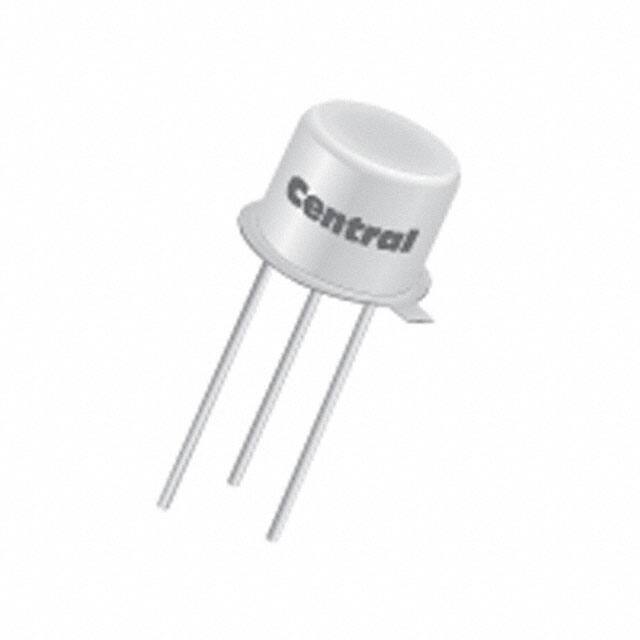


TRANS NPN 15V TO18
2N2369 is a high-speed switching transistor. This article enforces pinout, datasheet, equivalent, features, replacement, and more details about 2N2369. Furthermore, there is a huge range of semiconductors, capacitors, resistors, and Ics in stock. Welcome your RFQ!

Fainal transmmiter fm 500 mwatt MPSH10 2N2369A
2N2369 Pinout

2N2369 Pinout
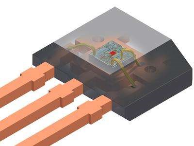
2N2369 CAD Model
Symbol

2N2369 Symbol
Footprint

2N2369 Footprint
What is 2N2369?
2N2369 is a TO-18 metal that can package with through-hole silicon planar epitaxial NPN high-speed switching transistors. This transistor has a low saturation voltage, quick switching, and a short turn-off. Low-power, high-speed saturation switching is a common application.

Specifications
- TypeParameter
- Lifecycle Status
Lifecycle Status refers to the current stage of an electronic component in its product life cycle, indicating whether it is active, obsolete, or transitioning between these states. An active status means the component is in production and available for purchase. An obsolete status indicates that the component is no longer being manufactured or supported, and manufacturers typically provide a limited time frame for support. Understanding the lifecycle status is crucial for design engineers to ensure continuity and reliability in their projects.
IN PRODUCTION (Last Updated: 1 month ago) - Factory Lead Time12 Weeks
- Contact Plating
Contact plating (finish) provides corrosion protection for base metals and optimizes the mechanical and electrical properties of the contact interfaces.
Lead, Tin - Mount
In electronic components, the term "Mount" typically refers to the method or process of physically attaching or fixing a component onto a circuit board or other electronic device. This can involve soldering, adhesive bonding, or other techniques to secure the component in place. The mounting process is crucial for ensuring proper electrical connections and mechanical stability within the electronic system. Different components may have specific mounting requirements based on their size, shape, and function, and manufacturers provide guidelines for proper mounting procedures to ensure optimal performance and reliability of the electronic device.
Through Hole - Mounting Type
The "Mounting Type" in electronic components refers to the method used to attach or connect a component to a circuit board or other substrate, such as through-hole, surface-mount, or panel mount.
Through Hole - Package / Case
refers to the protective housing that encases an electronic component, providing mechanical support, electrical connections, and thermal management.
TO-206AA, TO-18-3 Metal Can - Number of Pins3
- Transistor Element Material
The "Transistor Element Material" parameter in electronic components refers to the material used to construct the transistor within the component. Transistors are semiconductor devices that amplify or switch electronic signals and are a fundamental building block in electronic circuits. The material used for the transistor element can significantly impact the performance and characteristics of the component. Common materials used for transistor elements include silicon, germanium, and gallium arsenide, each with its own unique properties and suitability for different applications. The choice of transistor element material is crucial in designing electronic components to meet specific performance requirements such as speed, power efficiency, and temperature tolerance.
SILICON - Collector-Emitter Breakdown Voltage15V
- Number of Elements1
- Operating Temperature
The operating temperature is the range of ambient temperature within which a power supply, or any other electrical equipment, operate in. This ranges from a minimum operating temperature, to a peak or maximum operating temperature, outside which, the power supply may fail.
-65°C~200°C TJ - Packaging
Semiconductor package is a carrier / shell used to contain and cover one or more semiconductor components or integrated circuits. The material of the shell can be metal, plastic, glass or ceramic.
Bulk - Published2002
- JESD-609 Code
The "JESD-609 Code" in electronic components refers to a standardized marking code that indicates the lead-free solder composition and finish of electronic components for compliance with environmental regulations.
e0 - Pbfree Code
The "Pbfree Code" parameter in electronic components refers to the code or marking used to indicate that the component is lead-free. Lead (Pb) is a toxic substance that has been widely used in electronic components for many years, but due to environmental concerns, there has been a shift towards lead-free alternatives. The Pbfree Code helps manufacturers and users easily identify components that do not contain lead, ensuring compliance with regulations and promoting environmentally friendly practices. It is important to pay attention to the Pbfree Code when selecting electronic components to ensure they meet the necessary requirements for lead-free applications.
no - Part Status
Parts can have many statuses as they progress through the configuration, analysis, review, and approval stages.
Active - Moisture Sensitivity Level (MSL)
Moisture Sensitivity Level (MSL) is a standardized rating that indicates the susceptibility of electronic components, particularly semiconductors, to moisture-induced damage during storage and the soldering process, defining the allowable exposure time to ambient conditions before they require special handling or baking to prevent failures
1 (Unlimited) - Number of Terminations3
- ECCN Code
An ECCN (Export Control Classification Number) is an alphanumeric code used by the U.S. Bureau of Industry and Security to identify and categorize electronic components and other dual-use items that may require an export license based on their technical characteristics and potential for military use.
EAR99 - Terminal Finish
Terminal Finish refers to the surface treatment applied to the terminals or leads of electronic components to enhance their performance and longevity. It can improve solderability, corrosion resistance, and overall reliability of the connection in electronic assemblies. Common finishes include nickel, gold, and tin, each possessing distinct properties suitable for various applications. The choice of terminal finish can significantly impact the durability and effectiveness of electronic devices.
TIN LEAD - Max Power Dissipation
The maximum power that the MOSFET can dissipate continuously under the specified thermal conditions.
360mW - Terminal Position
In electronic components, the term "Terminal Position" refers to the physical location of the connection points on the component where external electrical connections can be made. These connection points, known as terminals, are typically used to attach wires, leads, or other components to the main body of the electronic component. The terminal position is important for ensuring proper connectivity and functionality of the component within a circuit. It is often specified in technical datasheets or component specifications to help designers and engineers understand how to properly integrate the component into their circuit designs.
BOTTOM - Terminal Form
Occurring at or forming the end of a series, succession, or the like; closing; concluding.
WIRE - Pin Count
a count of all of the component leads (or pins)
3 - Configuration
The parameter "Configuration" in electronic components refers to the specific arrangement or setup of the components within a circuit or system. It encompasses how individual elements are interconnected and their physical layout. Configuration can affect the functionality, performance, and efficiency of the electronic system, and may influence factors such as signal flow, impedance, and power distribution. Understanding the configuration is essential for design, troubleshooting, and optimizing electronic devices.
SINGLE - Power Dissipation
the process by which an electronic or electrical device produces heat (energy loss or waste) as an undesirable derivative of its primary action.
360mW - Case Connection
Case Connection refers to the method by which an electronic component's case or housing is connected to the electrical circuit. This connection is important for grounding purposes, mechanical stability, and heat dissipation. The case connection can vary depending on the type of component and its intended application. It is crucial to ensure a secure and reliable case connection to maintain the overall performance and safety of the electronic device.
COLLECTOR - Transistor Application
In the context of electronic components, the parameter "Transistor Application" refers to the specific purpose or function for which a transistor is designed and used. Transistors are semiconductor devices that can amplify or switch electronic signals and are commonly used in various electronic circuits. The application of a transistor can vary widely depending on its design and characteristics, such as whether it is intended for audio amplification, digital logic, power control, or radio frequency applications. Understanding the transistor application is important for selecting the right type of transistor for a particular circuit or system to ensure optimal performance and functionality.
SWITCHING - Polarity/Channel Type
In electronic components, the parameter "Polarity/Channel Type" refers to the characteristic that determines the direction of current flow or the type of signal that can be accommodated by the component. For components like diodes and transistors, polarity indicates the direction in which current can flow through the component, such as forward bias or reverse bias for diodes. For components like MOSFETs or JFETs, the channel type refers to whether the component is an N-channel or P-channel device, which determines the type of charge carriers that carry current through the component. Understanding the polarity or channel type of a component is crucial for proper circuit design and ensuring that the component is connected correctly to achieve the desired functionality.
NPN - Transistor Type
Transistor type refers to the classification of transistors based on their operation and construction. The two primary types are bipolar junction transistors (BJTs) and field-effect transistors (FETs). BJTs use current to control the flow of current, while FETs utilize voltage to control current flow. Each type has its own subtypes, such as NPN and PNP for BJTs, and MOSFETs and JFETs for FETs, impacting their applications and characteristics in electronic circuits.
NPN - Collector Emitter Voltage (VCEO)
Collector-Emitter Voltage (VCEO) is a key parameter in electronic components, particularly in transistors. It refers to the maximum voltage that can be applied between the collector and emitter terminals of a transistor while the base terminal is open or not conducting. Exceeding this voltage limit can lead to breakdown and potential damage to the transistor. VCEO is crucial for ensuring the safe and reliable operation of the transistor within its specified limits. Designers must carefully consider VCEO when selecting transistors for a circuit to prevent overvoltage conditions that could compromise the performance and longevity of the component.
15V - Max Collector Current
Max Collector Current is a parameter used to specify the maximum amount of current that can safely flow through the collector terminal of a transistor or other electronic component without causing damage. It is typically expressed in units of amperes (A) and is an important consideration when designing circuits to ensure that the component operates within its safe operating limits. Exceeding the specified max collector current can lead to overheating, degradation of performance, or even permanent damage to the component. Designers must carefully consider this parameter when selecting components and designing circuits to ensure reliable and safe operation.
400nA - DC Current Gain (hFE) (Min) @ Ic, Vce
The parameter "DC Current Gain (hFE) (Min) @ Ic, Vce" in electronic components refers to the minimum value of the DC current gain, denoted as hFE, under specific operating conditions of collector current (Ic) and collector-emitter voltage (Vce). The DC current gain hFE represents the ratio of the collector current to the base current in a bipolar junction transistor (BJT), indicating the amplification capability of the transistor. The minimum hFE value at a given Ic and Vce helps determine the transistor's performance and efficiency in amplifying signals within a circuit. Designers use this parameter to ensure proper transistor selection and performance in various electronic applications.
20 @ 100mA 1V - Vce Saturation (Max) @ Ib, Ic
The parameter "Vce Saturation (Max) @ Ib, Ic" in electronic components refers to the maximum voltage drop across the collector-emitter junction when the transistor is in saturation mode. This parameter is specified at a certain base current (Ib) and collector current (Ic) levels. It indicates the minimum voltage required to keep the transistor fully conducting in saturation mode, ensuring that the transistor operates efficiently and does not enter the cutoff region. Designers use this parameter to ensure proper transistor operation and to prevent overheating or damage to the component.
450mV @ 10mA, 100mA - Transition Frequency
Transition Frequency in electronic components refers to the frequency at which a device can transition from one state to another, typically defining the upper limit of its operating frequency. It is a critical parameter in determining the speed and performance of active components like transistors and integrated circuits. This frequency is influenced by factors such as capacitance, resistance, and the inherent characteristics of the materials used in the component's construction. Understanding transition frequency is essential for optimizing circuit designs and ensuring reliable signal processing in various applications.
500MHz - Collector Base Voltage (VCBO)
Collector Base Voltage (VCBO) is the maximum allowable voltage that can be applied between the collector and base terminals of a bipolar junction transistor when the emitter is open. It is a critical parameter that determines the voltage rating of the transistor and helps prevent breakdown in the collector-base junction. Exceeding this voltage can lead to permanent damage or failure of the component.
40V - Emitter Base Voltage (VEBO)
Emitter Base Voltage (VEBO) is a parameter used in electronic components, particularly in transistors. It refers to the maximum voltage that can be applied between the emitter and base terminals of a transistor without causing damage to the device. Exceeding this voltage limit can lead to breakdown of the transistor and potential failure. VEBO is an important specification to consider when designing circuits to ensure the proper operation and reliability of the components. It is typically provided in the datasheet of the transistor and should be carefully observed to prevent any potential damage during operation.
4.5V - VCEsat-Max
VCEsat-Max refers to the maximum collector-emitter saturation voltage of a bipolar junction transistor (BJT) or an insulated gate bipolar transistor (IGBT). It is a crucial parameter that indicates the minimum voltage drop across the collector-emitter junction when the transistor is in saturation mode. This parameter is important for determining the efficiency and performance of the transistor in switching applications. A lower VCEsat-Max value indicates better performance and reduced power losses in the transistor during operation. Designers often consider this parameter when selecting transistors for applications where minimizing power dissipation is critical.
0.45 V - Collector-Base Capacitance-Max
The parameter "Collector-Base Capacitance-Max" refers to the maximum capacitance that can exist between the collector and base terminals of a semiconductor device, such as a transistor. This capacitance is a result of the physical structure and material properties of the device and can have an impact on its performance in high-frequency applications. In practical terms, this parameter represents the maximum amount of charge that can be stored in the collector-base junction when a voltage is applied between the collector and base terminals. It is an important consideration in circuit design, especially in applications where high-speed switching or high-frequency operation is required, as excessive capacitance can lead to signal distortion or reduced performance.Manufacturers provide this specification to help engineers and designers understand the behavior of the device in different operating conditions and to ensure that the component meets the requirements of the intended application. It is typically measured in picofarads (pF) and is an essential parameter to consider when selecting components for high-frequency circuits.
4pF - Radiation Hardening
Radiation hardening is the process of making electronic components and circuits resistant to damage or malfunction caused by high levels of ionizing radiation, especially for environments in outer space (especially beyond the low Earth orbit), around nuclear reactors and particle accelerators, or during nuclear accidents or nuclear warfare.
No - RoHS Status
RoHS means “Restriction of Certain Hazardous Substances” in the “Hazardous Substances Directive” in electrical and electronic equipment.
Non-RoHS Compliant - Lead Free
Lead Free is a term used to describe electronic components that do not contain lead as part of their composition. Lead is a toxic material that can have harmful effects on human health and the environment, so the electronics industry has been moving towards lead-free components to reduce these risks. Lead-free components are typically made using alternative materials such as silver, copper, and tin. Manufacturers must comply with regulations such as the Restriction of Hazardous Substances (RoHS) directive to ensure that their products are lead-free and environmentally friendly.
Contains Lead
2N2369 Features
Bipolar (BJT) transistor
Transistor Type: NPN
Current - Collector (Ic) (Max): 200mA
Voltage - Collector Emitter Breakdown (Max): 15V
Vce Saturation (Max) @ Ib, Ic: 500mV @ 10mA, 100mA
Current - Collector Cutoff (Max): 400nA (ICBO)
DC Current Gain (hFE) (Min) @ Ic, Vce: 40 @ 10mA, 350mV
Power - Max: 360mW
Frequency - Transition: 500MHz
Operating Temperature: -65°C to 200°C (TJ)
Mounting Type: Through Hole
Package / Case: TO-18-3 Metal Can
2N2369 Application
The 2N2369 is used to amplify or switch electronic signals and electrical power. It is composed of semiconductor material and has at least three terminals for connecting to a circuit outside of it.
2N2369 Replacement
2N2221, 2N2222, BC378, BC378-6 or BC378-7
2N2369 Alternatives
| Part | Compare | Manufacturers | Category | Description |
| JAN2N2369A | Current Part | Microsemi | BJTs | Trans GP BJT NPN 15V 360mW 3Pin TO-18 |
| JANTX2N2369A | JAN2N2369A VS JANTX2N2369A | Microsemi | BJTs | Trans GP BJT NPN 15V 360mW 3Pin TO-18 |
| JANS2N2369A | JAN2N2369A VS JANS2N2369A | Microsemi | BJTs | TO-18 NPN 15V |
| 2N2369ALEADFREE | JAN2N2369A VS 2N2369ALEADFREE | Central Semiconductor | TO-18 NPN 15V 0.2A |
2N2369 Package Dimensions

2N2369 Package Dimensions
2N2369 Manufacturer
Microsemi Corporation (Nasdaq: MSCC) is a company dedicated to supplying prominent semiconductor and system solutions portfolios that serving in the field of aerospace & defense, communications, data center, and industrial markets. The products that we provide are not only containing high-performance and radiation-resistant analog mixed-signal integrated circuits, FPGAs, SoCs, and ASICs; power management products; but also timing and synchronization devices and precise time solutions to set world time standards and speech processing equipment. In addition, we also provide RF solutions; discrete components; enterprise storage and communication solutions, security technologies, and scalable tamper-proof products; Ethernet solutions; Power-over-Ethernet ICs and mid-spans; and custom design capabilities and services.
Trend Analysis
Datasheet PDF
- Datasheets :
What is 2N2369?
2N2369 is a semiconductor device used to amplify or switch electronic signals and electrical power. It is composed of semiconductor material usually with at least three terminals for connection to an external circuit. A voltage or current applied to one pair of the transistor's terminals controls the current through another pair of terminals. Because the controlled (output) power can be higher than the controlling (input) power, a transistor can amplify a signal. Today, some transistors are packaged individually, but many more are found embedded in integrated circuits.
What is 2N2369 used for?
2N2369 is a semiconductor device used to amplify or switch electronic signals and electrical power.
How does 2N2369 work?
The 2N2369 is a through-the-hole, silicon planar epitaxial NPN high-speed switching transistors in a TO-18 metal can package. This transistor features fast switching, short turn-off, and low saturation voltage. Typical applications are low power, high speed saturated switching.
Can 2N2369 replace 9018?
No. 2369 has a high withstand voltage of 50V and a current of 0.2A, whereas No. 9018 has a withstand voltage of 30V and a current of 0.05A.
 Exploring the Microchip PIC16C6X 8-Bit CMOS Microcontrollers
29 February 2024231
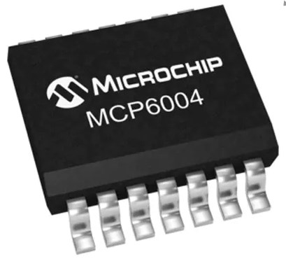 Microchip MCP6004-ISL Rail to Rail,3V,5V,14-Pin SOIC: Datasheet, Pinout, 3D Model
17 January 20222055
 TBA820M Amplifier: Datasheet, Circuit, Alternative
28 October 20215748
 A Comprehensive Guide to S-24CS64A0I-J8T1G EEPROM Memory Module
07 March 2024410
![LTC4054 Single-cell Lithium-ion Battery: Circuits, Pinout, and Datasheet [Video]](https://res.utmel.com/Images/Article/a849e0f4-9fdc-4e4e-9f76-e520361f732a.png) LTC4054 Single-cell Lithium-ion Battery: Circuits, Pinout, and Datasheet [Video]
LTC4054 Single-cell Lithium-ion Battery: Circuits, Pinout, and Datasheet [Video]04 January 202214570
 LP5018RSMR LED Driver: Datasheet, Alternatives, CAD Models
23 March 20222116
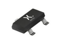 PMBTA42 Transistor: NPN High-Voltage, SOT23, Datasheet, Pinout
14 February 20221538
 ATmega328P Series: 8-bit AVR Microcontroller Design Guide
15 January 2026502
 Working Principle and Types of Electric Fuse
16 January 202615387
 Tunnel Diode: Definition, Features and Tunneling Process
25 August 202010247
 Introduction to Flyback Transformer
29 January 202111131
 Spiral wrap choices that keep hoses damage free
15 July 2025614
 What is GND in a Circuit?
18 December 202542945
 Tough Times for Japanese Component Manufacturers
10 August 20222831
 Basic Introduction to Hall Effect Sensors
13 November 20258504
 Hall Effect: Definition, Principle, Measurement Methods
08 November 20229037
Microsemi Corporation
In Stock
United States
China
Canada
Japan
Russia
Germany
United Kingdom
Singapore
Italy
Hong Kong(China)
Taiwan(China)
France
Korea
Mexico
Netherlands
Malaysia
Austria
Spain
Switzerland
Poland
Thailand
Vietnam
India
United Arab Emirates
Afghanistan
Åland Islands
Albania
Algeria
American Samoa
Andorra
Angola
Anguilla
Antigua & Barbuda
Argentina
Armenia
Aruba
Australia
Azerbaijan
Bahamas
Bahrain
Bangladesh
Barbados
Belarus
Belgium
Belize
Benin
Bermuda
Bhutan
Bolivia
Bonaire, Sint Eustatius and Saba
Bosnia & Herzegovina
Botswana
Brazil
British Indian Ocean Territory
British Virgin Islands
Brunei
Bulgaria
Burkina Faso
Burundi
Cabo Verde
Cambodia
Cameroon
Cayman Islands
Central African Republic
Chad
Chile
Christmas Island
Cocos (Keeling) Islands
Colombia
Comoros
Congo
Congo (DRC)
Cook Islands
Costa Rica
Côte d’Ivoire
Croatia
Cuba
Curaçao
Cyprus
Czechia
Denmark
Djibouti
Dominica
Dominican Republic
Ecuador
Egypt
El Salvador
Equatorial Guinea
Eritrea
Estonia
Eswatini
Ethiopia
Falkland Islands
Faroe Islands
Fiji
Finland
French Guiana
French Polynesia
Gabon
Gambia
Georgia
Ghana
Gibraltar
Greece
Greenland
Grenada
Guadeloupe
Guam
Guatemala
Guernsey
Guinea
Guinea-Bissau
Guyana
Haiti
Honduras
Hungary
Iceland
Indonesia
Iran
Iraq
Ireland
Isle of Man
Israel
Jamaica
Jersey
Jordan
Kazakhstan
Kenya
Kiribati
Kosovo
Kuwait
Kyrgyzstan
Laos
Latvia
Lebanon
Lesotho
Liberia
Libya
Liechtenstein
Lithuania
Luxembourg
Macao(China)
Madagascar
Malawi
Maldives
Mali
Malta
Marshall Islands
Martinique
Mauritania
Mauritius
Mayotte
Micronesia
Moldova
Monaco
Mongolia
Montenegro
Montserrat
Morocco
Mozambique
Myanmar
Namibia
Nauru
Nepal
New Caledonia
New Zealand
Nicaragua
Niger
Nigeria
Niue
Norfolk Island
North Korea
North Macedonia
Northern Mariana Islands
Norway
Oman
Pakistan
Palau
Palestinian Authority
Panama
Papua New Guinea
Paraguay
Peru
Philippines
Pitcairn Islands
Portugal
Puerto Rico
Qatar
Réunion
Romania
Rwanda
Samoa
San Marino
São Tomé & Príncipe
Saudi Arabia
Senegal
Serbia
Seychelles
Sierra Leone
Sint Maarten
Slovakia
Slovenia
Solomon Islands
Somalia
South Africa
South Sudan
Sri Lanka
St Helena, Ascension, Tristan da Cunha
St. Barthélemy
St. Kitts & Nevis
St. Lucia
St. Martin
St. Pierre & Miquelon
St. Vincent & Grenadines
Sudan
Suriname
Svalbard & Jan Mayen
Sweden
Syria
Tajikistan
Tanzania
Timor-Leste
Togo
Tokelau
Tonga
Trinidad & Tobago
Tunisia
Turkey
Turkmenistan
Turks & Caicos Islands
Tuvalu
U.S. Outlying Islands
U.S. Virgin Islands
Uganda
Ukraine
Uruguay
Uzbekistan
Vanuatu
Vatican City
Venezuela
Wallis & Futuna
Yemen
Zambia
Zimbabwe
![JAN2N3724UB]() JAN2N3724UB
JAN2N3724UBMicrosemi
![2N718]() 2N718
2N718Microsemi
![2N3501e3]() 2N3501e3
2N3501e3Microsemi
![2N7372]() 2N7372
2N7372Microsemi
![2N3700UB/TR]() 2N3700UB/TR
2N3700UB/TRMicrosemi
![JANTXV2N918UB/TR]() JANTXV2N918UB/TR
JANTXV2N918UB/TRMicrosemi
![Jantxv2N6211]() Jantxv2N6211
Jantxv2N6211Microsemi
![Jantxv2N3700UB/TR]() Jantxv2N3700UB/TR
Jantxv2N3700UB/TRMicrosemi
![JANS2N2369AUB-TR]() JANS2N2369AUB-TR
JANS2N2369AUB-TRMicrosemi
![JANS2N2221AUBC/TR]() JANS2N2221AUBC/TR
JANS2N2221AUBC/TRMicrosemi
