
 Product
 Brand
Brand Articles
 Tools
Tools
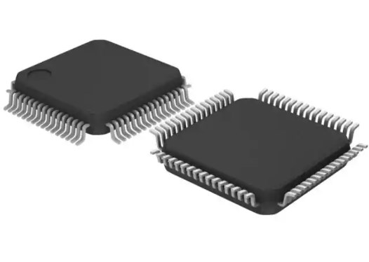
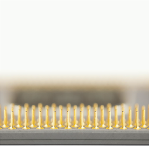
XC7K160T-2FFG676I AMD/Xilinx FPGA: Detailed Specifications and Features


3.37mm mm FPGAs Kintex®-7 Series 676-BBGA, FCBGA 1mm mm 676
The XC7K160T-2FFG676I is a powerful chip in the Kintex-7 family. Made with 28nm technology, it works fast and processes data well. It has 12,675 logic blocks, 600 DSP slices, and 400 user I/Os. This makes it great for tough jobs in telecom, aerospace, and medical tools. Its design is strong and handles hard tasks easily. The datasheet shows features that make it flexible and efficient. If you need fast data work or steady performance, this FPGA is a great choice.
Specifications
- TypeParameter
- Factory Lead Time10 Weeks
- Mounting Type
The "Mounting Type" in electronic components refers to the method used to attach or connect a component to a circuit board or other substrate, such as through-hole, surface-mount, or panel mount.
Surface Mount - Package / Case
refers to the protective housing that encases an electronic component, providing mechanical support, electrical connections, and thermal management.
676-BBGA, FCBGA - Surface Mount
having leads that are designed to be soldered on the side of a circuit board that the body of the component is mounted on.
YES - Number of I/Os400
- Operating Temperature
The operating temperature is the range of ambient temperature within which a power supply, or any other electrical equipment, operate in. This ranges from a minimum operating temperature, to a peak or maximum operating temperature, outside which, the power supply may fail.
-40°C~100°C TJ - Packaging
Semiconductor package is a carrier / shell used to contain and cover one or more semiconductor components or integrated circuits. The material of the shell can be metal, plastic, glass or ceramic.
Tray - Series
In electronic components, the "Series" refers to a group of products that share similar characteristics, designs, or functionalities, often produced by the same manufacturer. These components within a series typically have common specifications but may vary in terms of voltage, power, or packaging to meet different application needs. The series name helps identify and differentiate between various product lines within a manufacturer's catalog.
Kintex®-7 - Published2009
- JESD-609 Code
The "JESD-609 Code" in electronic components refers to a standardized marking code that indicates the lead-free solder composition and finish of electronic components for compliance with environmental regulations.
e1 - Pbfree Code
The "Pbfree Code" parameter in electronic components refers to the code or marking used to indicate that the component is lead-free. Lead (Pb) is a toxic substance that has been widely used in electronic components for many years, but due to environmental concerns, there has been a shift towards lead-free alternatives. The Pbfree Code helps manufacturers and users easily identify components that do not contain lead, ensuring compliance with regulations and promoting environmentally friendly practices. It is important to pay attention to the Pbfree Code when selecting electronic components to ensure they meet the necessary requirements for lead-free applications.
yes - Part Status
Parts can have many statuses as they progress through the configuration, analysis, review, and approval stages.
Active - Moisture Sensitivity Level (MSL)
Moisture Sensitivity Level (MSL) is a standardized rating that indicates the susceptibility of electronic components, particularly semiconductors, to moisture-induced damage during storage and the soldering process, defining the allowable exposure time to ambient conditions before they require special handling or baking to prevent failures
4 (72 Hours) - Number of Terminations676
- ECCN Code
An ECCN (Export Control Classification Number) is an alphanumeric code used by the U.S. Bureau of Industry and Security to identify and categorize electronic components and other dual-use items that may require an export license based on their technical characteristics and potential for military use.
3A991.D - Terminal Finish
Terminal Finish refers to the surface treatment applied to the terminals or leads of electronic components to enhance their performance and longevity. It can improve solderability, corrosion resistance, and overall reliability of the connection in electronic assemblies. Common finishes include nickel, gold, and tin, each possessing distinct properties suitable for various applications. The choice of terminal finish can significantly impact the durability and effectiveness of electronic devices.
Tin/Silver/Copper (Sn96.5Ag3.0Cu0.5) - HTS Code
HTS (Harmonized Tariff Schedule) codes are product classification codes between 8-1 digits. The first six digits are an HS code, and the countries of import assign the subsequent digits to provide additional classification. U.S. HTS codes are 1 digits and are administered by the U.S. International Trade Commission.
8542.39.00.01 - Voltage - Supply
Voltage - Supply refers to the range of voltage levels that an electronic component or circuit is designed to operate with. It indicates the minimum and maximum supply voltage that can be applied for the device to function properly. Providing supply voltages outside this range can lead to malfunction, damage, or reduced performance. This parameter is critical for ensuring compatibility between different components in a circuit.
0.97V~1.03V - Terminal Position
In electronic components, the term "Terminal Position" refers to the physical location of the connection points on the component where external electrical connections can be made. These connection points, known as terminals, are typically used to attach wires, leads, or other components to the main body of the electronic component. The terminal position is important for ensuring proper connectivity and functionality of the component within a circuit. It is often specified in technical datasheets or component specifications to help designers and engineers understand how to properly integrate the component into their circuit designs.
BOTTOM - Terminal Form
Occurring at or forming the end of a series, succession, or the like; closing; concluding.
BALL - Supply Voltage
Supply voltage refers to the electrical potential difference provided to an electronic component or circuit. It is crucial for the proper operation of devices, as it powers their functions and determines performance characteristics. The supply voltage must be within specified limits to ensure reliability and prevent damage to components. Different electronic devices have specific supply voltage requirements, which can vary widely depending on their design and intended application.
1V - Terminal Pitch
The center distance from one pole to the next.
1mm - Base Part Number
The "Base Part Number" (BPN) in electronic components serves a similar purpose to the "Base Product Number." It refers to the primary identifier for a component that captures the essential characteristics shared by a group of similar components. The BPN provides a fundamental way to reference a family or series of components without specifying all the variations and specific details.
XC7K160 - Pin Count
a count of all of the component leads (or pins)
676 - JESD-30 Code
JESD-30 Code refers to a standardized descriptive designation system established by JEDEC for semiconductor-device packages. This system provides a systematic method for generating designators that convey essential information about the package's physical characteristics, such as size and shape, which aids in component identification and selection. By using JESD-30 codes, manufacturers and engineers can ensure consistency and clarity in the specification of semiconductor packages across various applications and industries.
S-PBGA-B676 - Number of Outputs400
- Power Supplies
an electronic circuit that converts the voltage of an alternating current (AC) into a direct current (DC) voltage.?
11.83.3V - RAM Size
RAM size refers to the amount of random access memory (RAM) available in an electronic component, such as a computer or smartphone. RAM is a type of volatile memory that stores data and instructions that are actively being used by the device's processor. The RAM size is typically measured in gigabytes (GB) and determines how much data the device can store and access quickly for processing. A larger RAM size allows for smoother multitasking, faster loading times, and better overall performance of the electronic component. It is an important factor to consider when choosing a device, especially for tasks that require a lot of memory, such as gaming, video editing, or running multiple applications simultaneously.
1.4MB - Clock Frequency
Clock frequency, also known as clock speed, refers to the rate at which a processor or electronic component can execute instructions. It is measured in hertz (Hz) and represents the number of cycles per second that the component can perform. A higher clock frequency typically indicates a faster processing speed and better performance. However, it is important to note that other factors such as architecture, efficiency, and workload also play a significant role in determining the overall performance of a component. In summary, clock frequency is a crucial parameter that influences the speed and efficiency of electronic components in processing data and executing tasks.
1286MHz - Propagation Delay
the flight time of packets over the transmission link and is limited by the speed of light.
100 ps - Number of Inputs400
- Programmable Logic Type
Generally, programmable logic devices can be described as being one of three different types: Simple programmable logic devices (SPLD) Complex programmable logic devices (CPLD) Field programmable logic devices (FPGA).
FIELD PROGRAMMABLE GATE ARRAY - Number of Logic Elements/Cells162240
- Total RAM Bits
Total RAM Bits refers to the total number of memory bits that can be stored in a Random Access Memory (RAM) component. RAM is a type of computer memory that allows data to be accessed in any random order, making it faster than other types of memory like hard drives. The total RAM bits indicate the capacity of the RAM chip to store data temporarily for quick access by the computer's processor. The more total RAM bits a component has, the more data it can store and process at any given time, leading to improved performance and multitasking capabilities.
11980800 - Number of LABs/CLBs12675
- Speed Grade
Speed grade is a specification in electronic components that indicates the maximum operating speed at which the component can reliably function. It is commonly used for integrated circuits, particularly in digital logic devices and programmable logic devices. The speed grade is typically denoted by a number or letter code that correlates to the maximum frequency or propagation delay of the device, influencing its performance in high-speed applications. Components with higher speed grades are capable of faster processing and lower signal delay compared to those with lower grades.
-2 - Number of Registers202800
- Combinatorial Delay of a CLB-Max
The Combinatorial Delay of a CLB-Max in electronic components refers to the time it takes for a signal to propagate through a combinational logic block (CLB) within a Field-Programmable Gate Array (FPGA) to reach its output. This delay is influenced by factors such as the complexity of the logic function being implemented, the routing resources available, and the physical distance the signal needs to travel within the CLB. Understanding and optimizing the Combinatorial Delay of a CLB-Max is crucial in designing efficient and high-performance digital circuits, as it directly impacts the overall speed and functionality of the FPGA design. By minimizing this delay, designers can achieve faster operation and improved performance in their electronic systems.
0.61 ns - Length27mm
- Height Seated (Max)
Height Seated (Max) is a parameter in electronic components that refers to the maximum allowable height of the component when it is properly seated or installed on a circuit board or within an enclosure. This specification is crucial for ensuring proper fit and alignment within the overall system design. Exceeding the maximum seated height can lead to mechanical interference, electrical shorts, or other issues that may impact the performance and reliability of the electronic device. Manufacturers provide this information to help designers and engineers select components that will fit within the designated space and function correctly in the intended application.
3.37mm - Width27mm
- Radiation Hardening
Radiation hardening is the process of making electronic components and circuits resistant to damage or malfunction caused by high levels of ionizing radiation, especially for environments in outer space (especially beyond the low Earth orbit), around nuclear reactors and particle accelerators, or during nuclear accidents or nuclear warfare.
No - RoHS Status
RoHS means “Restriction of Certain Hazardous Substances” in the “Hazardous Substances Directive” in electrical and electronic equipment.
ROHS3 Compliant
Overview of the XC7K160 FPGA
Introduction to the Kintex-7 family
The Kintex-7 family by Xilinx is known for being affordable, efficient, and fast. These FPGAs are made with advanced 28nm technology. This makes them quicker and uses less power. The Kintex-7 series works well for jobs needing fast data handling and steady communication. Its design includes features like built-in clock control and fast data links. This makes it useful for many industries.
Key attributes of the XC7K160T-2FFG676I
The XC7K160T-2FFG676I FPGA has amazing features. It has 160,000 logic cells, 660 DSP slices, and 5,760 KB of memory. These make it great for hard math tasks and storing data. It also has 32 fast data links for smooth communication. The FPGA runs on 1.0V and works in temperatures from -40°C to +100°C. This wide range makes it reliable in tough conditions.
| Attribute | Details |
|---|---|
| Number of Logic Cells | 160,000 |
| On-Chip Memory | 5,760 KB |
| Number of DSP Slices | 660 |
| Number of High-Speed Transceivers | 32 |
| Operating Voltage | 1.0V |
| Operating Temperature Range | -40°C to +100°C |
General use cases and target industries
The XC7K160 FPGA can be used in many ways. Its fast data links and strong design are great for wireless systems and video tasks. It is also used in factories where accuracy is important. In aerospace, it works well in extreme conditions. Its low cost makes it a good choice for data centers and small devices.
Tip: If you work in telecom, aerospace, or factories, the XC7K160T-2FFG676I FPGA might be the right tool for your project.
Detailed Specifications of the XC7K160T-2FFG676I
Logic cells, LUTs, and DSP slices
The xc7k160t-2ffg676i FPGA has many useful features. It includes 160,000 logic cells, which help build digital circuits. These cells let you create custom hardware for your needs. The FPGA also has advanced 6-input LUTs. These make logic tasks faster and save resources. With 660 DSP slices, it handles math tasks like signal processing easily. This mix of features makes it great for tough computing jobs.
Memory resources and block RAM
Memory is very important for how an FPGA works. The xc7k160t-2ffg676i has 5,760 KB of block RAM. This memory stores and accesses data quickly during tasks. Block RAM is fast and handles big datasets well. It also supports distributed RAM for more memory options. Whether for image work, machine learning, or real-time data, this FPGA’s memory ensures smooth performance.
Power consumption and thermal characteristics
Saving power is important, and this FPGA does it well. It runs on 1.0V, using less energy but staying strong. It works in temperatures from -40°C to +100°C. This means it can handle tough environments like factories or space. Good thermal management helps it last longer and work better.
Operating voltage and temperature range
The XC7K160T-2FFG676I FPGA works well in many situations. It uses a core voltage of 1.0V. This helps it save energy and work efficiently. Its design focuses on using less power, which is great for projects needing low energy use.
Another great feature is its wide temperature range. It works in places as cold as -40°C or as hot as +100°C. This makes it useful in tough environments like factories or space. The strong thermal design keeps it steady and reliable, even in hard conditions.
To avoid overheating, the FPGA has special cooling features. These help it stay cool and last longer. If you’re building systems for harsh places, this FPGA is a smart choice.
Note: Always check your FPGA’s working conditions for best results. Good cooling and voltage control can make it even more reliable.
The XC7K160T-2FFG676I’s ability to handle extreme temperatures and save energy makes it very flexible. Whether for telecom, medical tools, or factory systems, this FPGA fits your needs easily.
Key Features of the XC7K160 FPGA
High-speed transceivers and I/O capabilities
The xc7k160t-2ffg676i FPGA has fast serial transceivers. These allow data speeds up to 12.5 Gbps. This makes it great for quick communication in telecom and networking. It handles fast data tasks easily. Its memory interface works well with external devices. This improves system performance and speed.
This FPGA has 400 user I/Os for connecting devices. These I/Os support different voltage levels. This helps it fit into many systems. Whether for signal processing or fast communication, this FPGA is reliable and efficient.
Scalability and flexibility for diverse applications
The xc7k160 FPGA is built to grow with your needs. Its design lets you expand and customize as projects change. With 160,000 logic cells and 660 DSP slices, it handles complex tasks. You can use it for advanced math or machine learning.
It supports modular designs, so you can reuse parts in new projects. It works well with Xilinx tools, making design easier. Whether for small prototypes or big systems, this FPGA adjusts to your needs and performs well.
Support for industry-standard protocols
The xc7k160t-2ffg676i FPGA works with many standard protocols. It supports SerDes interfaces like PCIe and Ethernet for fast connections. It also works with DDR3 and DDR4 memory for modern systems.
Its strong DSP features help with precise tasks like communication. These protocol supports make it easy to add to existing systems. This saves time and lowers costs. Its tough design ensures it works well in hard conditions.
Tip: Choose the xc7k160 FPGA for projects needing fast data and advanced processing. Its features make it a smart choice.
| Metric | Description |
|---|---|
| LUTmin | Smallest LUT usage in successful designs. |
| Automation | Automates checks for correctness and resource use. |
| Resource Metrics | Tracks LUT, DSP, and register use during synthesis. |
| Reporting | Creates reports on pass rates and resource stats. |
| Visualization | Compares correctness and resource efficiency automatically. |
2D NoC tech for quick data movement with low power.
Improved DSP and ML arrays for strong, efficient computing.
Supports fast SerDes (up to 112 Gbps) and modern memory (GDDR6, DDR5).
Advanced 6-input LUT technology
The XC7K160T-2FFG676I FPGA uses special 6-input LUTs for better performance. A Look-Up Table (LUT) is an important part of an FPGA. It stores answers for logic tasks based on input combinations. Most older FPGAs use 4-input LUTs, but this one uses 6-input LUTs.
Why is this helpful? A 6-input LUT can handle harder logic tasks in one step. This means fewer LUTs are needed in your design. Using fewer LUTs saves resources and makes processing faster. You get better results without losing speed or power.
Here’s how it helps your work:
Improved Logic Density: One 6-input LUT can do the job of many 4-input LUTs. This increases how much logic the FPGA can handle.
Faster Performance: With fewer LUTs in the way, designs work faster. This is important for tasks needing quick results.
Lower Power Use: Using fewer resources means less energy is needed. This makes your designs more efficient.
Tip: If your project needs fast data or tough algorithms, this 6-input LUT tech can make your design simpler and faster.
| Feature | Benefit |
|---|---|
| 6-input LUT | Handles harder logic tasks in fewer steps |
| Higher Logic Density | Uses fewer LUTs for the same task |
| Faster Signal Processing | Speeds up how the system works |
This technology makes your designs strong and ready for modern needs. Whether you’re working on telecom, factories, or medical tools, the 6-input LUTs in the XC7K160T-2FFG676I FPGA give you the power and flexibility you need.
Pinout and Configuration
Overview of the FFG676 package
The FFG676 package is small and well-designed to hold the XC7K160T-2FFG676I FPGA. It has 676 pins arranged in a ball grid array (BGA) format. This setup allows many connections while keeping the size small. The package supports fast data transfer and works reliably. It is perfect for tasks needing strong communication and processing. Its design also helps manage heat, keeping it stable in tough conditions.
Pin layout and signal assignments
Knowing the pin layout is important for using the FPGA in your system. Each pin in the FFG676 package has a specific job, like powering the chip or sending data. Below is a table showing key pin functions:
| Pin Name | Description | Function |
|---|---|---|
| VCCINT | Internal voltage | Powers the internal logic |
| VCCAUX | Auxiliary voltage | Powers extra functions and I/O |
| GND | Ground | Connects to ground for stability |
| IO | I/O pins | Links to external devices |
| CLK | Clock input | Provides timing for operations |
| RESET | Reset input | Resets the logic to its starting state |
| CONFIG | Configuration pins | Used for programming and setup |
This pin layout makes it easy to connect with other devices. Special pins for power, clock, and reset simplify the design and improve reliability.
Configuration options and programming methods
Setting up the XC7K160T-2FFG676I FPGA means picking the right programming method. You can choose from JTAG programming, serial configuration, or flash memory boot. Each method has its own benefits, like being fast, flexible, or simple.
Manufacturers provide helpful guides and tools for setup. For example, resources like "MAX® 10 FPGA Developer Center" and "Simulation Quick-Start for ModelSim-Intel FPGA Edition" give step-by-step instructions. These guides cover design, testing, and verification. Using them ensures your setup is correct and works well.
Tip: Always test your setup with simulation tools before using the FPGA in your system. This helps avoid mistakes and ensures it works properly.
The XC7K160T-2FFG676I FPGA offers flexible setup and programming options. Whether you’re working on telecom, factory systems, or aerospace projects, this FPGA fits your needs easily.
Applications of the XC7K160T-2FFG676I FPGA
Telecommunications and networking
The XC7K160T-2FFG676I FPGA is great for fast communication systems. It processes data at speeds up to 12.5 Gbps. This makes it perfect for modern telecom networks like 5G. It handles tasks such as signal encoding, decoding, and fixing errors. These features help keep communication smooth and reliable.
This FPGA works with protocols like Ethernet and PCIe. These allow it to fit easily into current systems. Its design can grow to handle more data as needed. For example, during testing, it reached over 800 MB/s per slot at 300 MHz. This shows how well it manages large data in cost-friendly ways.
Aerospace and defense
In aerospace, systems need to be strong and precise. The XC7K160T-2FFG676I FPGA meets these needs with its tough design. It works in extreme temperatures from -40°C to +100°C. This makes it reliable for radar, satellites, and avionics.
For example, it checks system status using digital and analog inputs during tests. This improves safety in aerospace testing. It also works in EO/IR imaging systems, handling complex signals and data. These features make it a trusted choice for important aerospace projects.
Industrial automation and control
The XC7K160T-2FFG676I FPGA is key for factory automation. Its fast transceivers and 400 I/Os connect many devices and sensors. This is important for real-time monitoring and controlling machines.
Its low power use and smart design make it cost-effective. It helps improve processes, reduce downtime, and boost productivity. Whether for robots or smart factories, this FPGA offers the performance and flexibility you need.
Tip: For industrial projects, use this FPGA for fast communication and control. It can greatly improve system performance.
Medical imaging and diagnostics
The XC7K160T-2FFG676I FPGA helps improve medical imaging systems. Its fast processing and flexible design make it great for handling medical data. This FPGA boosts the accuracy of tools like MRI, CT scans, and ultrasounds.
A key feature is its ability to handle large data quickly. Medical devices create huge datasets that need fast analysis. With 660 DSP slices and 5,760 KB of block RAM, this FPGA processes data smoothly. It helps create clearer images and better diagnostic results.
Did you know? The advanced 6-input LUT technology uses fewer resources. This makes image processing faster and more efficient.
This FPGA works with protocols like PCIe and Ethernet. These help connect imaging systems to other devices easily. Its 400 user I/Os allow it to work with many sensors and tools. Whether for portable ultrasounds or advanced MRI machines, this FPGA fits your needs.
| Feature | Benefit for Medical Imaging |
|---|---|
| High-speed transceivers | Faster data transfer and analysis |
| 6-input LUT technology | Efficient image reconstruction |
| Wide temperature range | Reliable in diverse environments |
The XC7K160T-2FFG676I FPGA also saves power. Medical devices often run nonstop, so energy-saving features lower costs and heat. This keeps systems reliable and long-lasting.
By using this FPGA, you can make medical imaging tools better. This leads to more accurate results and improved patient care.
Advantages and Disadvantages of the XC7K160 FPGA
Advantages of the XC7K160T-2FFG676I
The xc7k160t-2ffg676i has a great mix of features. It has 160,000 logic cells and 660 DSP slices. These make it perfect for fast data tasks. Its advanced 6-input LUTs improve logic density. This helps create faster and better designs. With 5,760 KB of memory, it handles big data easily. This makes it useful for medical tools and factory systems.
This FPGA also has high-speed transceivers. They can send data at 12.5 Gbps. These are great for telecom and networking. It works in temperatures from -40°C to +100°C. This makes it reliable in tough places like space or defense. It also uses less power, saving energy and money.
Tip: If you want a Xilinx FPGA that is fast and energy-saving, choose the xc7k160t-2ffg676i.
Potential limitations and challenges
The xc7k160 FPGA is strong but has limits. Its 160,000 logic cells may not be enough for very complex tasks. For example, jobs needing lots of parallel processing might need more logic cells. Also, its 5,760 KB memory is good for most tasks but may not work for memory-heavy jobs like advanced AI.
Another issue is its 32 high-speed transceivers. This number might not be enough for systems needing many fast connections. Plus, the FPGA and its tools can be costly. This could be hard for small projects or startups.
Note: Always check your project needs to see if this FPGA fits.
Comparison with other FPGA families
Compared to other Xilinx models, the xc7k160t-2ffg676i is balanced. For example, the xc7k325t-2ffg676i has 325,000 logic cells and 11,520 KB memory. This makes it better for very complex tasks. But the xc7k160t-2ffg676i is cheaper and uses less energy. It’s great for medium-complexity projects.
| Feature | XC7K160T-2FFG676I | XC7K325T-2FFG676I |
|---|---|---|
| Logic Cells | 160,000 | 325,000 |
| On-chip Memory | 5,760 KB | 11,520 KB |
| DSP Slices | 660 | 1,080 |
| High-speed Transceivers | 32 | 48 |
The xc7k160t-2ffg676i is energy-saving and flexible. It’s a smart pick for projects needing good performance without extra resources.
Package and Manufacturer Details
FFG676 package dimensions and specifications
The FFG676 package is small and works well. It uses a ball grid array (BGA) design with 676 pins. This setup makes strong connections and allows fast data transfer. The package size is about 27mm x 27mm, which fits tight spaces. Its design also helps manage heat, keeping it steady in tough tasks. This package is great for jobs needing strong communication and processing.
Manufacturer support and documentation
AMD-Xilinx gives lots of help for the xc7k160t-2ffg676i. You can find datasheets, guides, and notes to learn about the FPGA. These resources explain both simple setups and advanced features. For example, Intel (Altera) shares guides and updates, while Achronix provides notes and papers. ON Semiconductor also offers helpful documents for your designs. These tools make it easier to use the FPGA fully.
| Vendor | Type of Document | Description |
|---|---|---|
| Intel (Altera) | Support Resources | Guides and updates for FPGA features and use. |
| Achronix | Documentation | Notes, datasheets, guides, and white papers for FPGA users. |
Availability and sourcing
You can easily find the xc7k160t-2ffg676i from many sellers. Buy it from trusted vendors to get real products and good service. Many sellers also give tech help for using the FPGA in your projects. Always check the datasheet and vendor info to pick the right version. Getting it from reliable sources ensures good quality and performance for your needs.
Comparisons with Similar FPGAs
Comparison with other Kintex-7 models
The xc7k160t-2ffg676i has unique strengths in the Kintex-7 family. The XC7A200T has more logic cells, which helps with complex designs. But the xc7k160t-2ffg676i is better for fast communication tasks due to its transceivers. The Virtex-7 series offers higher performance and logic density. However, it uses more power and costs more. For a cheaper option, the Spartan-7 is good. Yet, it lacks the speed and logic power of the xc7k160t-2ffg676i.
Tip: Pick the xc7k160t-2ffg676i if you need speed, logic, and energy savings.
Comparison with competing FPGAs from other manufacturers
The xc7k160t-2ffg676i also shines against FPGAs from other brands. Intel’s Stratix series is powerful but uses more energy and costs more. Altera’s Cyclone series is affordable but lacks advanced features and fast transceivers. Achronix’s Speedster FPGAs are great for AI but less flexible for general tasks.
Cost-performance analysis
The xc7k160t-2ffg676i balances cost and performance well. Below is a table comparing cost and energy efficiency with similar products:
| Metric | Alveo U50 | GeForce RTX 3090 | Other GPU |
|---|---|---|---|
| Throughput (Events/s) | 0.55 | 1.10 | 0.82 |
| Active Power Draw (W) | 75 | 350 | 230 |
| Energy per Event (μJ) | 140 | 430 | 210 |
| Price (USD) | 1500 | 3000 | ~10000 |
| Annual Operating Cost (EUR) | 120 | 380 | N/A |
| Cost Efficiency Gain | 3.1x | 1.0x | N/A |
This table shows how the xc7k160t-2ffg676i saves energy and money. It’s a smart choice for high-performance projects without high costs.
The xc7k160t-2ffg676i FPGA is a strong and dependable chip. It has 160,000 logic cells, 660 DSP slices, and 5,760 KB of RAM. These features make it work well for tough tasks. Its fast transceivers and wide temperature range are great for telecom, space, and factories.
Scientists at CERN and Lawrence Berkeley Lab showed how FPGAs handle data fast. They also work well for machine learning, making them very useful today.
If you need a chip that saves energy and works hard, this FPGA is a smart pick for your project.
Parts with Similar Specs
- ImagePart NumberManufacturerPackage / CaseNumber of InputsNumber of Logic Elements/CellsNumber of I/ORAM SizeSupply VoltagePbfree CodeTerminal FinishView Compare
![XC7K160T-2FFG676I]()
XC7K160T-2FFG676I
676-BBGA, FCBGA
400
162240
400
1.4 MB
1 V
yes
Tin/Silver/Copper (Sn96.5Ag3.0Cu0.5)
![XC6VCX130T-1FFG784C]()
784-BBGA, FCBGA
-
128000
400
1.2 MB
1 V
yes
Tin/Silver/Copper (Sn96.5Ag3.0Cu0.5)


Datasheet PDF
- Datasheets :
- PCN Design/Specification :
- PCN Assembly/Origin :
- Environmental Information :
 Technical Deep Dive: ADuC7030/ADuC7033 Integrated Precision Battery Sensor
29 February 2024158
 LM2902DG Op-Amp: Pinout, Equivalent and Datasheet
06 December 20213331
 IRF644 Power MOSFET: Datasheet, Pinout, Test Circuit
25 September 20213183
 A Comprehensive Guide to LTC7815EUHF#TRPBF DC DC Switching Controller
06 March 2024189
 MCP3208 Analog to Digital Converters: Pinout, Datasheet, and Applications
11 September 20218689
![CDSOT23-SM712 Tvs Diode Surface SOT-23-3 14V Clamp[FAQ]: Datasheet, Pinout, and Applications](https://res.utmel.com/Images/Article/9fea5c62-7b3d-490f-89eb-f71899f86d2b.png) CDSOT23-SM712 Tvs Diode Surface SOT-23-3 14V Clamp[FAQ]: Datasheet, Pinout, and Applications
CDSOT23-SM712 Tvs Diode Surface SOT-23-3 14V Clamp[FAQ]: Datasheet, Pinout, and Applications02 April 20222601
![An Overview of L298N Motor Driver [Video]](https://res.utmel.com/Images/Article/6925db0e-74c0-4aca-ad94-431f22fa7bce.png) An Overview of L298N Motor Driver [Video]
An Overview of L298N Motor Driver [Video]11 May 202110686
 STM32F302R8T6 Microcontroller: Pinout, Datasheet, and Specification
29 June 20213558
 Semiconductor Market Expected to Surge, Driven by Rising Number of Data Centers
04 June 20242852
 What is 232\485\422 Communication? Common problems of Serial Communication
29 April 20222516
 How much do you know about CPU?
07 February 20222668
 The Rise of Semiconductor Stocks in the Tech Boom
05 December 20233995
 What is a USB Flash Drive?
25 May 20213490
 Using Microcontrollers in the Internet of Things (IoT) Applications
27 June 20236515
 What is Inter-Integrated Circuit (I2C)?
23 February 20223802
 What is Graphics Processing Unit (GPU)?
18 October 20218069
Xilinx Inc.
In Stock: 495
United States
China
Canada
Japan
Russia
Germany
United Kingdom
Singapore
Italy
Hong Kong(China)
Taiwan(China)
France
Korea
Mexico
Netherlands
Malaysia
Austria
Spain
Switzerland
Poland
Thailand
Vietnam
India
United Arab Emirates
Afghanistan
Åland Islands
Albania
Algeria
American Samoa
Andorra
Angola
Anguilla
Antigua & Barbuda
Argentina
Armenia
Aruba
Australia
Azerbaijan
Bahamas
Bahrain
Bangladesh
Barbados
Belarus
Belgium
Belize
Benin
Bermuda
Bhutan
Bolivia
Bonaire, Sint Eustatius and Saba
Bosnia & Herzegovina
Botswana
Brazil
British Indian Ocean Territory
British Virgin Islands
Brunei
Bulgaria
Burkina Faso
Burundi
Cabo Verde
Cambodia
Cameroon
Cayman Islands
Central African Republic
Chad
Chile
Christmas Island
Cocos (Keeling) Islands
Colombia
Comoros
Congo
Congo (DRC)
Cook Islands
Costa Rica
Côte d’Ivoire
Croatia
Cuba
Curaçao
Cyprus
Czechia
Denmark
Djibouti
Dominica
Dominican Republic
Ecuador
Egypt
El Salvador
Equatorial Guinea
Eritrea
Estonia
Eswatini
Ethiopia
Falkland Islands
Faroe Islands
Fiji
Finland
French Guiana
French Polynesia
Gabon
Gambia
Georgia
Ghana
Gibraltar
Greece
Greenland
Grenada
Guadeloupe
Guam
Guatemala
Guernsey
Guinea
Guinea-Bissau
Guyana
Haiti
Honduras
Hungary
Iceland
Indonesia
Iran
Iraq
Ireland
Isle of Man
Israel
Jamaica
Jersey
Jordan
Kazakhstan
Kenya
Kiribati
Kosovo
Kuwait
Kyrgyzstan
Laos
Latvia
Lebanon
Lesotho
Liberia
Libya
Liechtenstein
Lithuania
Luxembourg
Macao(China)
Madagascar
Malawi
Maldives
Mali
Malta
Marshall Islands
Martinique
Mauritania
Mauritius
Mayotte
Micronesia
Moldova
Monaco
Mongolia
Montenegro
Montserrat
Morocco
Mozambique
Myanmar
Namibia
Nauru
Nepal
New Caledonia
New Zealand
Nicaragua
Niger
Nigeria
Niue
Norfolk Island
North Korea
North Macedonia
Northern Mariana Islands
Norway
Oman
Pakistan
Palau
Palestinian Authority
Panama
Papua New Guinea
Paraguay
Peru
Philippines
Pitcairn Islands
Portugal
Puerto Rico
Qatar
Réunion
Romania
Rwanda
Samoa
San Marino
São Tomé & Príncipe
Saudi Arabia
Senegal
Serbia
Seychelles
Sierra Leone
Sint Maarten
Slovakia
Slovenia
Solomon Islands
Somalia
South Africa
South Sudan
Sri Lanka
St Helena, Ascension, Tristan da Cunha
St. Barthélemy
St. Kitts & Nevis
St. Lucia
St. Martin
St. Pierre & Miquelon
St. Vincent & Grenadines
Sudan
Suriname
Svalbard & Jan Mayen
Sweden
Syria
Tajikistan
Tanzania
Timor-Leste
Togo
Tokelau
Tonga
Trinidad & Tobago
Tunisia
Turkey
Turkmenistan
Turks & Caicos Islands
Tuvalu
U.S. Outlying Islands
U.S. Virgin Islands
Uganda
Ukraine
Uruguay
Uzbekistan
Vanuatu
Vatican City
Venezuela
Wallis & Futuna
Yemen
Zambia
Zimbabwe
![XC6SLX45-2FGG484C]() XC6SLX45-2FGG484C
XC6SLX45-2FGG484CXilinx Inc.
![XC3S400-4PQG208I]() XC3S400-4PQG208I
XC3S400-4PQG208IXilinx Inc.
![XC6SLX9-2CSG225I]() XC6SLX9-2CSG225I
XC6SLX9-2CSG225IXilinx Inc.
![XCV1000-4BG560C]() XCV1000-4BG560C
XCV1000-4BG560CXilinx Inc.
![XC5VFX130T-2FFG1738I]() XC5VFX130T-2FFG1738I
XC5VFX130T-2FFG1738IXilinx Inc.
![XCV50E-7FG256I]() XCV50E-7FG256I
XCV50E-7FG256IXilinx Inc.
![XC2S400E-6FGG456C]() XC2S400E-6FGG456C
XC2S400E-6FGG456CXilinx Inc.
![XC2S100E-6FT256C]() XC2S100E-6FT256C
XC2S100E-6FT256CXilinx Inc.
![XC2S15-5CS144C]() XC2S15-5CS144C
XC2S15-5CS144CXilinx Inc.
![XCS10-3VQG100C]() XCS10-3VQG100C
XCS10-3VQG100CXilinx Inc.


