Comprehensive Analysis of Switching Power Supply Circuits

How Does a Switching Power Supply Work 1 (schematic, explanation, example, modifications)
Catalog |
01 Circuit composition of switching power supply
The main circuit of a switching power supply is composed of an input electromagnetic interference filter (EMI), a rectifier filter circuit, a power conversion circuit, a PWM controller circuit, and an output rectifier filter circuit. Auxiliary circuits include input overvoltage and under-voltage protection circuits, output overvoltage and under-voltage protection circuits, output overcurrent protection circuits, and output short-circuit protection circuits.
The block diagram of the circuit composition of the switching power supply is as follows:

Switching power supply circuit block diagram
02 Principle of the input circuit and common circuit
1 Principle of AC input rectifier filter circuit

Input filter, rectifier circuit schematic diagram
① Lightning protection circuit: When there is a lightning strike, high voltage is generated and imported into the power supply through the power grid. A circuit composed of MOV1, MOV2, MOV3: F1, F2, F3, FDG1 is used for protection. When the voltage applied to both ends of the varistor exceeds its working voltage, its resistance is reduced, causing high-voltage energy to be consumed on the varistor. If the current is too large, F1, F2, F3 will burn down the protection circuit.
② Input filter circuit: The double π-type filter network composed of C1, L1, C2 and C3 mainly suppresses the electromagnetic noise and clutter signal of the input power supply, preventing interference to the power supply. It also prevents the high-frequency clutter generated by the power source from interfering with the power grid. When the power is turned on, the C5 should be charged. Due to the large instantaneous current, adding RT1 (thermistor) can effectively prevent surge current. Because the instantaneous energy is all consumed in the RT1 resistance, the temperature rises after a certain period of time, and the resistance value of RT1 decreases (RT1 is a negative temperature coefficient component). At this time, it consumes very little energy, and the subsequent circuit can work normally.
③ Rectification and filter circuit: After the AC voltage is rectified by BRG1, it is filtered by C5 to obtain a relatively pure DC voltage. If the C5 capacity becomes smaller, the output AC ripple will increase.
2 Principle of DC input filter circuit
①Input filter circuit: The double π-type filter network composed of C1, L1, and C2 mainly suppresses the electromagnetic noise and clutter signal of the input power supply, preventing interference to the power supply. At the same time, it also prevents high-frequency clutter generated by the power supply from interfering with the power grid. C3 and C4 are safety capacitors, and L2 and L3 are differential mode inductors.
② R1, R2, R3, Z1, C6, Q1, Z2, R4, R5, Q2, RT1, C7 form an anti-surge circuit. At the moment of starting, Q2 does not conduct due to the presence of C6, and the current forms a loop through RT1. When the voltage on C6 is charged to the regulated value of Z1, Q2 turns on. If C8 leaks or the subsequent circuit is short-circuited. At the moment of the startup, the voltage drop generated by the current on RT1 increases, and Q1 turns on, so that Q2 does not have a gate voltage and does not turn on, and RT1 will burn in a short time to protect the subsequent circuit.
03 Power Conversion Circuit
1 MOSFET working principle
At present, the most widely used insulated gate field effect transistor is the MOSFET, which uses the electroacoustic effect of the semiconductor surface. MOSFET is also called a surface field-effect device. Since its gate is in a non-conductive state, the input resistance can be greatly increased, up to 105 ohms. MOSFET uses the magnitude of the gate-source voltage to change the amount of charge induced on the semiconductor surface, thereby controlling the magnitude of the drain current.
2 Common schematics
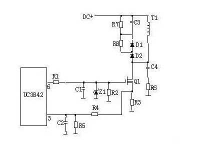
Schematic diagram of the power conversion circuit
3 Working principle
R4, C3, R5, R6, C4, D1, D2 form a buffer. It is connected in parallel with the switch MOSFET so that the voltage stress of the switch tube is reduced, EMI is reduced, and no secondary breakdown occurs. When the switching tube Q1 is turned off, the primary coil of the transformer is prone to spike voltage and spike current. The combination of these components can well absorb peak voltage and current. The current peak signal measured from R3 participates in the duty cycle control of the current working cycle, so it is the current limit of the current working cycle.
When the voltage on R5 reaches 1V, UC3842 stops working, and the switch Q1 turns off immediately. The junction capacitances CGS and CGD in R1 and Q1 form an RC network together. The charging and discharging of the capacitor directly affects the switching speed of the switch tube. If R1 is too small, it is easy to cause oscillation and electromagnetic interference will be great; if R1 is too large, it will reduce the switching speed of the switch tube. Z1 usually limits the GS voltage of the MOS tube to below 18V, thereby protecting the MOS tube.
The gate-controlled voltage of Q1 is a saw-shaped wave. When the duty cycle is larger, the longer conduction time of Q1, the more energy stored in the transformer; when Q1 is turned off, the transformer release energy through D1, D2, R5, R4, C3. At the same time, the purpose of magnetic field reset is achieved, and it is ready for the next storage and transfer of energy of the transformer. The IC constantly adjusts the duty cycle of the ⑥ pin saw wave according to the output voltage and current, thereby stabilizing the output current and voltage of the whole machine. C4 and R6 are spike voltage absorption loops.
4 Push-pull power conversion circuit
Q1 and Q2 will turn on in turn.
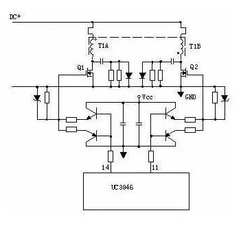
The push-pull power conversion circuit
5 Power conversion circuit with drive transformer
T2 is the drive transformer, T1 is the switching transformer, and TR1 is the current loop.
04 Output rectifier filter circuit
1 Forward rectifier circuit
T1 is a switching transformer, and the phases of its primary and secondary poles are in phase. D1 is a rectifier diode, D2 is a freewheeling diode, and R1, C1, R2, and C2 are peak sharpening circuits. L1 is a freewheeling inductor, and C4, L2, and C5 form a π-type filter.
2 Flyback rectifier circuit
T1 is a switching transformer, and the phases of the primary and secondary poles are opposite. D1 is a rectifier diode, R1 and C1 are peak-shaving circuits. L1 is a freewheeling inductor, R2 is a dummy load, and C4, L2, and C5 form a π-type filter.
3 Synchronous rectifier circuit
Working principle: When the upper end of the transformer secondary is positive, the current makes Q2 conduct through C2, R5, R6, R7, the circuit forms a loop. Q2 is a rectifier tube. The gate of Q1 is turned off due to the reverse bias. When the lower end of the transformer secondary is positive, the current flows through C3, R4, and R2 to make Q1 conductive, and Q1 is a freewheeling tube. The gate of Q2 is turned off due to the reverse bias. L2 is a freewheeling inductor, and C6, L1, and C7 form a π-type filter. R1, C1, R9, and C4 are peak clipping circuits.
05 Principle of Voltage Stabilization Loop
1 Schematic diagram of the feedback circuit
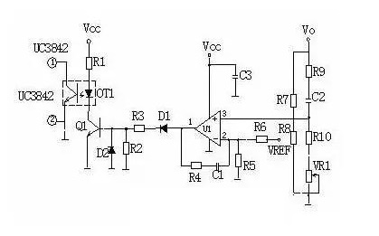
2 Working principle
When the output U0 rises, after being divided by the sampling resistors R7, R8, R10, and VR1, the voltage at pin U1③ rises. When the voltage of pin U1③ exceeds the reference voltage of pin U1②, pin U1① outputs a high level. Q1 is turned on, the light-emitting diode of the optocoupler OT1 emits light, and the phototransistor is turned on. The potential of the UC3842 ① pin becomes lower accordingly, thereby changing the output duty cycle of the U1 ⑥ pin to decrease and U0 to decrease.
When the output U0 decreases, the voltage at pin U1 ③ decreases. When the voltage of U1③ is lower than the reference voltage of U1②, U1① outputs low level. Q1 does not conduct, the light-emitting diode of the optocoupler OT1 does not emit light, and the phototransistor does not conduct. UC3842 ① pin potential rises, thus changing U1 ⑥ pin output duty cycle increases, U0 decreases. Repeatedly, so that the output voltage remains stable. Adjust VR1 to change the output voltage value.
The feedback loop is an important circuit that affects the stability of the switching power supply. For example, the feedback resistance and capacitance are wrong, leaking, and false welding, etc., will produce self-excited oscillation. The fault phenomenon is abnormal waveform, empty or full load oscillation, unstable output voltage, etc.
06 Short circuit protection circuit
1. When the output terminal is short-circuited, the PWM control circuit can limit the output current within a safe range, and it can use a variety of methods to realize the current limiting circuit. When the power current limit does not work in a short circuit, only a part of the circuit is added.
2. There are usually two types of short-circuit protection circuits. The figure below is a low-power short-circuit protection circuit. The principle is briefly described as follows:
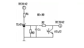
Low power short circuit protection circuit
When the output circuit is short-circuited, the output voltage disappears and the optocoupler OT1 does not conduct. The voltage of the UC3842① pin rises to about 5V, and the partial pressure of R1 and R2 exceeds the TL431 reference, making it conductive. UC3842⑦ pin VCC potential is pulled low, IC stops working. After the UC3842 stops working, the potential of the pin disappears, and the TL431 is not turned on. The potential of the UC3842 rises, and the UC3842 restarts, repeating the cycle. When the short-circuit phenomenon disappears, the circuit can automatically return to the normal working state.
07 Output current limit protection
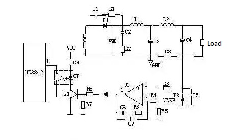
Output current limiting protection circuit
The above figure is a common output current limiting protection circuit, and its working principle is briefly described as the above figure: when the output current is too large, the voltage across RS (manganese copper wire) rises. The voltage at pin U1③ is higher than the reference voltage at pin ②, and pin U1① output high voltage. Q1 turns on, optocoupler produces the photoelectric effect. UC3842① pin voltage decreases, output voltage decreases, so as to achieve the purpose of output overload current limiting.
08 Principle of output overvoltage protection circuit
The function of the output overvoltage protection circuit is to limit the output voltage to a safe value when the output voltage exceeds the design value. When the internal voltage stabilization loop of the switching power supply fails or the output overvoltage is caused by improper operation by the user, the overvoltage protection circuit protects it to prevent damage to the subsequent electrical equipment. The most commonly used overvoltage protection circuits are as follows:
1 SCR trigger protection circuit
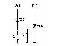
Thyristor trigger protection circuit
As shown in the figure above, when the output of Uo1 rises, the Zener tube (Z3) breaks down and turns on, and the control terminal of the SCR (SCR1) gets the trigger voltage, so the SCR turns on. When Uo2 voltage is short-circuited to the ground, the over-current protection circuit or the short-circuit protection circuit will work and stop the work of the entire power supply circuit. When the output overvoltage phenomenon is eliminated, the trigger voltage of the control terminal of the SCR is discharged to the ground through R, and the SCR returns to the disconnected state.
2 Photoelectric coupling protection circuit
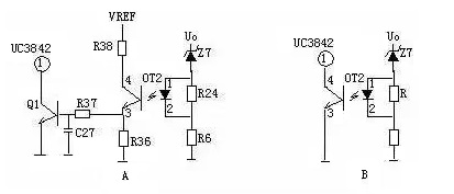
The photoelectric coupling protection circuit
As shown in the figure above, when Uo has an overvoltage phenomenon, the Zener tube breaks down and conducts. A current flows through the optocoupler (OT2) R6 to the ground, and the light-emitting diode of the photocoupler emits light so that the phototransistor of the photocoupler conducts. The base of Q1 is turned on, and the ③ pin of 3842 is reduced, which turns off the IC and stops the work of the entire power supply, and Uo is zero, and the cycle repeats.
3 Output voltage limit protection circuit
The output voltage limit protection circuit is shown in the figure below. When the output voltage rises, the voltage regulator tube is turned on and the optocoupler is turned on. The base of Q1 is turned on with the driving voltage, and the voltage of UC3842 ③ rises, and the output drops. The voltage regulator tube is not turned on, the voltage of UC3842 ③ decreases, and the output voltage increases. Repeatedly, the output voltage will stabilize within a range (depending on the voltage regulator value of the Zener tube).
4 Output overvoltage lockout circuit
The working principle of Figure A is that when the output voltage Uo rises, the Zener tube is turned on, the optocoupler is turned on, and the base of Q2 is turned on. As Q2 is turned on, the base voltage of Q1 is also turned on, and the Vcc voltage passes through R1, Q1, R2 make Q2 always on. UC3842 ③ pin is always high and stops working. In Figure B, UO rises, U1 ③ pin voltage rises, ① pin outputs high level. Due to the existence of D1 and R1, U1 ① pin always outputs high level and Q1 is always on. UC3842 ① pin is always low and stops working.
09 Power factor correction circuit (PFC)
1 Schematic diagram of the principle

Power factor correction circuit (PFC)
2 Working principle
The input voltage is passed through an EMI filter composed of L1, L2, L3, etc... BRG1 rectifies one route to the PFC inductor, and the other route is divided by R1 and R2 and sent to the PFC controller as a sampling of the input voltage to adjust the duty of the control signal Ratio, that is, change the turn-on and turn-off time of Q1 to stabilize the PFC output voltage. L4 is the PFC inductor, which stores energy when Q1 is turned on and releases energy when Q1 is turned off. D1 is the start diode. D2 is PFC rectifier diode, C6, C7 filter. The PFC voltage is sent to the post-stage circuit one way, and the other is sent to the PFC controller after being divided by R3 and R4 as a sampling of the PFC output voltage to adjust the duty cycle of the control signal and stabilize the PFC output voltage.
10 Input over-voltage protection
1 Schematic
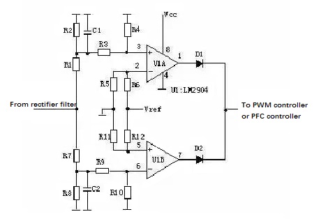
Input over voltage protection circuit
2 Working principle
The input overvoltage and under-voltage protection principles of AC input and DC input switching power supplies are roughly the same. The sampling voltage of the protection circuit comes from the voltage after input filtering. The sampling voltage is divided into two ways, one way is divided by R1, R2, R3, R4 and then input to the comparator 3 pin. If the sampling voltage is higher than the 2 pin reference voltage, the comparator 1 pin outputs a high level to control the main controller to make it turn off, the power supply has no output. The other is divided by R7, R8, R9, R10 and then input to the comparator 6 pin. If the sampling voltage is lower than the 5 pin reference voltage, the comparator 7 pin outputs a high level to control the main controller to turn off, and the power supply has no output.
1. How does a switching power supply work?
A switch mode supply works by turning the mains electricity on and off very quickly to reduce the voltage. In this case the reduction in voltage depends upon the ratio of the on time and off time. Switching takes place very fast, at 10,000 times a second or quicker.
2. What is power supply circuit?
A power supply is an electronic circuit designed to provide various ac and dc voltages for equipment operation. Low dc voltages are needed to operate ICs and transistors. High voltages are needed to operate CRTs and other devices. Batteries can provide all of these voltages.
 LLC Converter with Planar Matrix Transformer for High-Current-High-Power ApplicationsSaumitra Jagdale15 March 20244761
The rise of data centres in recent years, driven by cloud computing and big data, has caused a significant increase in electricity consumption. In the United States alone, it exceeded 70 billion kWh by 2014, making up 1.8% of total national electricity usage.
Read More Enhancing Frequency Stability in Modern Distributed Power SystemsRakesh Kumar, Ph.D.21 September 20244261
The article discusses the importance of primary frequency regulation in maintaining grid stability. It also explores battery energy storage systems, virtual synchronous generators, and advanced control strategies to enhance frequency stability in power systems.
Read More The Impact of SMPS on LED Lighting and Diverse IndustriesUTMEL05 June 20252615
Switched-Mode Power Supplies (SMPS) enhance LED lighting and industries by improving energy efficiency, reliability, and sustainability across diverse applications.
Read More What is Uninterruptible Power Supply (UPS)?UTMEL08 April 20215273
UPS is an uninterruptible power supply containing the energy storage device. It is mainly used to give a part of a device with a higher power stability, providing uninterrupted power supplies.
Read More Switch-mode Power Supply BasicsUTMEL14 December 20207883
Switched-mode Power Supply (SMPS), also known as switching converter, is a high-frequency electric energy conversion device and a type of power supply. Its function is to convert a level of voltage into the voltage or current required by the user through different forms of architecture.
Read More
Subscribe to Utmel !
![LY3F-AC120]() LY3F-AC120
LY3F-AC120Omron Automation and Safety
![JW2SN-DC9V]() JW2SN-DC9V
JW2SN-DC9VPanasonic Electric Works
![RGC1A60D60KGE]() RGC1A60D60KGE
RGC1A60D60KGECarlo Gavazzi Inc.
![JQ1P-24V]() JQ1P-24V
JQ1P-24VPanasonic Electric Works
![LY1-DC24]() LY1-DC24
LY1-DC24Omron Automation and Safety
![JVN1AF-12V-F]() JVN1AF-12V-F
JVN1AF-12V-FPanasonic Electric Works
![3RT20161AF01]() 3RT20161AF01
3RT20161AF01Siemens
![ADW1103W]() ADW1103W
ADW1103WPanasonic Electric Works
![3RH21222BM40]() 3RH21222BM40
3RH21222BM40Siemens
![3RT20241DB443MA0]() 3RT20241DB443MA0
3RT20241DB443MA0Siemens


 Product
 Brand
Brand Articles
 Tools
Tools


