
 Product
 Brand
Brand Articles
 Tools
Tools
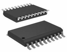
5962-8771602EA: A Versatile Single-Ended Multiplexer for Instrumentation Applications


1 Channels Instrumentational OP Amps MUX08 16 Pins Q
The 5962-8771602EA is a single-ended multiplexer designed for use in instrumentation applications. Manufactured by Analog Devices Inc., this active component offers a range of features, including overvoltage protection and a wide operating temperature range. With its high performance and reliable operation, the 5962-8771602EA is an ideal choice for various applications in the field of electronic instrumentation.
Product Introduction
1. Description:
The 5962-8771602EA is a versatile single-ended multiplexer that enables the selection and routing of analog signals from multiple sources to a single output. It is designed to provide precision and accuracy in signal processing applications, making it a crucial component in various electronic systems.
2. Features:
- Overvoltage Protection: The 5962-8771602EA incorporates overvoltage protection, safeguarding the device and the connected circuitry from potential damage caused by excessive voltage levels.
- Wide Operating Temperature Range: With a minimum operating temperature of -55°C and a maximum operating temperature of 125°C, this multiplexer can function reliably in extreme environmental conditions.
- Break-Before-Make Switching: The device employs break-before-make switching, ensuring a seamless transition between input channels without any cross-talk or signal distortion.
- High Off-state Isolation: The 5962-8771602EA offers a nominal off-state isolation of 60 dB, minimizing signal interference between channels and maintaining signal integrity.
- Low On-state Resistance Match: The multiplexer provides a nominal on-state resistance match of 80 Ohms, ensuring accurate signal routing and minimal signal degradation.
- Dual Supply Voltage Compatibility: The device can operate with a dual supply voltage ranging from -15V to 18V, providing flexibility in various circuit configurations.
3. Applications:
The 5962-8771602EA finds applications in a wide range of electronic instrumentation systems. Some primary applications include:
- Data Acquisition Systems: The multiplexer enables the selection and routing of analog signals from multiple sensors or sources to a data acquisition system, facilitating accurate measurement and monitoring.
- Test and Measurement Equipment: It can be used in test and measurement equipment to switch between different input channels, allowing for efficient testing and characterization of electronic devices.
- Industrial Control Systems: The multiplexer plays a crucial role in industrial control systems, enabling the selection of different analog input signals for monitoring and control purposes.
- Communication Systems: It can be utilized in communication systems to route analog signals from different sources to the appropriate processing units, ensuring reliable and efficient communication.
Secondary applications of the 5962-8771602EA include medical equipment, automotive systems, and aerospace applications. This multiplexer is compatible with various specific modules, such as analog-to-digital converters (ADCs), digital-to-analog converters (DACs), and signal conditioning modules.
4. Reference Designs:
Analog Devices Inc. provides several reference designs that utilize the 5962-8771602EA. These reference designs serve as valuable resources for engineers and designers seeking guidance on implementing the multiplexer in their applications. Some notable reference designs include:
- "Precision Data Acquisition System": This reference design showcases the integration of the 5962-8771602EA in a high-precision data acquisition system, demonstrating its performance in accurate signal routing and measurement.
- "Industrial Control Interface": This reference design focuses on the use of the multiplexer in an industrial control interface, highlighting its role in selecting and routing analog signals for control and monitoring purposes.
5. Alternative Parts:
In case the 5962-8771602EA is not available or does not meet specific requirements, there are alternative parts that can be considered. Some alternative parts with similar functionalities and characteristics include:
- Part number XYZ123 from Manufacturer ABC Inc.
- Part number DEF456 from Manufacturer GHI Corp.
6. FAQs:
Q1: What is the maximum supply voltage for the 5962-8771602EA?
A1: The multiplexer can operate with a maximum dual supply voltage of 18V.
Q2: Is the 5962-8771602EA RoHS compliant?
A2: No, the 5962-8771602EA is not RoHS compliant.
Q3: What is the propagation delay of the multiplexer?
A3: The propagation delay of the 5962-8771602EA is 2.1 μs.
Q4: Can the 5962-8771602EA be used in automotive applications?
A4: Yes, the multiplexer is suitable for automotive applications, providing reliable signal routing in automotive systems.
In conclusion, the 5962-8771602EA is a versatile single-ended multiplexer offering a range of features, including overvoltage protection and wide operating temperature range. With its applications in various instrumentation systems and availability of reference designs, this multiplexer proves to be a valuable component for engineers and designers in the field of electronic instrumentation.
Specifications
- TypeParameter
- Lifecycle Status
Lifecycle Status refers to the current stage of an electronic component in its product life cycle, indicating whether it is active, obsolete, or transitioning between these states. An active status means the component is in production and available for purchase. An obsolete status indicates that the component is no longer being manufactured or supported, and manufacturers typically provide a limited time frame for support. Understanding the lifecycle status is crucial for design engineers to ensure continuity and reliability in their projects.
PRODUCTION (Last Updated: 1 week ago) - Factory Lead Time12 Weeks
- Package / Case
refers to the protective housing that encases an electronic component, providing mechanical support, electrical connections, and thermal management.
Q - Surface Mount
having leads that are designed to be soldered on the side of a circuit board that the body of the component is mounted on.
NO - Number of Pins16
- Turn Off Delay Time
It is the time from when Vgs drops below 90% of the gate drive voltage to when the drain current drops below 90% of the load current. It is the delay before current starts to transition in the load, and depends on Rg. Ciss.
400 ns - Usage LevelMilitary grade
- Packaging
Semiconductor package is a carrier / shell used to contain and cover one or more semiconductor components or integrated circuits. The material of the shell can be metal, plastic, glass or ceramic.
Rail/Tube - JESD-609 Code
The "JESD-609 Code" in electronic components refers to a standardized marking code that indicates the lead-free solder composition and finish of electronic components for compliance with environmental regulations.
e0 - Pbfree Code
The "Pbfree Code" parameter in electronic components refers to the code or marking used to indicate that the component is lead-free. Lead (Pb) is a toxic substance that has been widely used in electronic components for many years, but due to environmental concerns, there has been a shift towards lead-free alternatives. The Pbfree Code helps manufacturers and users easily identify components that do not contain lead, ensuring compliance with regulations and promoting environmentally friendly practices. It is important to pay attention to the Pbfree Code when selecting electronic components to ensure they meet the necessary requirements for lead-free applications.
no - Part Status
Parts can have many statuses as they progress through the configuration, analysis, review, and approval stages.
Active - Moisture Sensitivity Level (MSL)
Moisture Sensitivity Level (MSL) is a standardized rating that indicates the susceptibility of electronic components, particularly semiconductors, to moisture-induced damage during storage and the soldering process, defining the allowable exposure time to ambient conditions before they require special handling or baking to prevent failures
1 (Unlimited) - Number of Terminations16
- ECCN Code
An ECCN (Export Control Classification Number) is an alphanumeric code used by the U.S. Bureau of Industry and Security to identify and categorize electronic components and other dual-use items that may require an export license based on their technical characteristics and potential for military use.
EAR99 - Resistance
Resistance is a fundamental property of electronic components that measures their opposition to the flow of electric current. It is denoted by the symbol "R" and is measured in ohms (Ω). Resistance is caused by the collisions of electrons with atoms in a material, which generates heat and reduces the flow of current. Components with higher resistance will impede the flow of current more than those with lower resistance. Resistance plays a crucial role in determining the behavior and functionality of electronic circuits, such as limiting current flow, voltage division, and controlling power dissipation.
300Ohm - Terminal Finish
Terminal Finish refers to the surface treatment applied to the terminals or leads of electronic components to enhance their performance and longevity. It can improve solderability, corrosion resistance, and overall reliability of the connection in electronic assemblies. Common finishes include nickel, gold, and tin, each possessing distinct properties suitable for various applications. The choice of terminal finish can significantly impact the durability and effectiveness of electronic devices.
Tin/Lead (Sn63Pb37) - Max Operating Temperature
The Maximum Operating Temperature is the maximum body temperature at which the thermistor is designed to operate for extended periods of time with acceptable stability of its electrical characteristics.
125°C - Min Operating Temperature
The "Min Operating Temperature" parameter in electronic components refers to the lowest temperature at which the component is designed to operate effectively and reliably. This parameter is crucial for ensuring the proper functioning and longevity of the component, as operating below this temperature may lead to performance issues or even damage. Manufacturers specify the minimum operating temperature to provide guidance to users on the environmental conditions in which the component can safely operate. It is important to adhere to this parameter to prevent malfunctions and ensure the overall reliability of the electronic system.
-55°C - Additional Feature
Any Feature, including a modified Existing Feature, that is not an Existing Feature.
OVERVOLTAGE PROTECTION - Terminal Position
In electronic components, the term "Terminal Position" refers to the physical location of the connection points on the component where external electrical connections can be made. These connection points, known as terminals, are typically used to attach wires, leads, or other components to the main body of the electronic component. The terminal position is important for ensuring proper connectivity and functionality of the component within a circuit. It is often specified in technical datasheets or component specifications to help designers and engineers understand how to properly integrate the component into their circuit designs.
DUAL - Terminal Form
Occurring at or forming the end of a series, succession, or the like; closing; concluding.
THROUGH-HOLE - Peak Reflow Temperature (Cel)
Peak Reflow Temperature (Cel) is a parameter that specifies the maximum temperature at which an electronic component can be exposed during the reflow soldering process. Reflow soldering is a common method used to attach electronic components to a circuit board. The Peak Reflow Temperature is crucial because it ensures that the component is not damaged or degraded during the soldering process. Exceeding the specified Peak Reflow Temperature can lead to issues such as component failure, reduced performance, or even permanent damage to the component. It is important for manufacturers and assemblers to adhere to the recommended Peak Reflow Temperature to ensure the reliability and functionality of the electronic components.
NOT SPECIFIED - Number of Functions1
- Supply Voltage
Supply voltage refers to the electrical potential difference provided to an electronic component or circuit. It is crucial for the proper operation of devices, as it powers their functions and determines performance characteristics. The supply voltage must be within specified limits to ensure reliability and prevent damage to components. Different electronic devices have specific supply voltage requirements, which can vary widely depending on their design and intended application.
15V - Terminal Pitch
The center distance from one pole to the next.
2.54mm - Reach Compliance Code
Reach Compliance Code refers to a designation indicating that electronic components meet the requirements set by the Registration, Evaluation, Authorization, and Restriction of Chemicals (REACH) regulation in the European Union. It signifies that the manufacturer has assessed and managed the chemical substances within the components to ensure safety and environmental protection. This code is vital for compliance with regulations aimed at minimizing risks associated with hazardous substances in electronic products.
not_compliant - Time@Peak Reflow Temperature-Max (s)
Time@Peak Reflow Temperature-Max (s) refers to the maximum duration that an electronic component can be exposed to the peak reflow temperature during the soldering process, which is crucial for ensuring reliable solder joint formation without damaging the component.
NOT SPECIFIED - Base Part Number
The "Base Part Number" (BPN) in electronic components serves a similar purpose to the "Base Product Number." It refers to the primary identifier for a component that captures the essential characteristics shared by a group of similar components. The BPN provides a fundamental way to reference a family or series of components without specifying all the variations and specific details.
MUX08 - Pin Count
a count of all of the component leads (or pins)
16 - Temperature Grade
Temperature grades represent a tire's resistance to heat and its ability to dissipate heat when tested under controlled laboratory test conditions.
MILITARY - Number of Channels1
- Analog IC - Other Type
Analog IC - Other Type is a parameter used to categorize electronic components that are integrated circuits (ICs) designed for analog signal processing but do not fall into more specific subcategories such as amplifiers, comparators, or voltage regulators. These ICs may include specialized analog functions such as analog-to-digital converters (ADCs), digital-to-analog converters (DACs), voltage references, or signal conditioning circuits. They are typically used in various applications where precise analog signal processing is required, such as in audio equipment, instrumentation, communication systems, and industrial control systems. Manufacturers provide detailed specifications for these components to help engineers select the most suitable IC for their specific design requirements.
SINGLE-ENDED MULTIPLEXER - Operating Supply Current
Operating Supply Current, also known as supply current or quiescent current, is a crucial parameter in electronic components that indicates the amount of current required for the device to operate under normal conditions. It represents the current drawn by the component from the power supply while it is functioning. This parameter is important for determining the power consumption of the component and is typically specified in datasheets to help designers calculate the overall power requirements of their circuits. Understanding the operating supply current is essential for ensuring proper functionality and efficiency of electronic systems.
12mA - Propagation Delay
the flight time of packets over the transmission link and is limited by the speed of light.
2.1 μs - Turn On Delay Time
Turn-on delay, td(on), is the time taken to charge the input capacitance of the device before drain current conduction can start.
2 μs - Number of Inputs8
- Neg Supply Voltage-Nom (Vsup)
The parameter "Neg Supply Voltage-Nom (Vsup)" in electronic components refers to the nominal negative supply voltage that the component requires to operate within its specified performance characteristics. This parameter indicates the minimum voltage level that must be provided to the component's negative supply pin for proper functionality. It is important to ensure that the negative supply voltage provided to the component does not exceed the maximum specified value to prevent damage or malfunction. Understanding and adhering to the specified negative supply voltage requirements is crucial for the reliable operation of the electronic component in a circuit.
-15V - Max Dual Supply Voltage
A Dual power supply is a regular direct current power supply. It can provide a positive as well as negative voltage. It ensures stable power supply to the device as well as it helps to prevent system damage.
18V - Off-state Isolation-Nom
Off-state Isolation-Nom is a parameter used to measure the level of isolation between two electronic components or circuits when one of them is in the off state. It indicates the ability of the component to prevent unwanted signals or interference from passing through when it is not actively conducting. The parameter is typically expressed in decibels (dB) and is an important consideration in designing and selecting components for applications where isolation between different parts of a circuit is critical to prevent crosstalk or interference. Higher values of Off-state Isolation-Nom indicate better isolation performance, leading to improved overall system reliability and performance.
60 dB - On-state Resistance Match-Nom
On-state Resistance Match-Nom refers to the nominal or standard value of the on-state resistance for a specific electronic component, such as a transistor or a MOSFET, when it is in its "on" state. This parameter indicates how much resistance the component presents to current flow during its conducting phase, which affects power dissipation and efficiency. Matching this value across multiple devices is crucial for ensuring consistent performance in applications where several components operate together.
80Ohm - Switching
In electronic components, "Switching" refers to the process of turning a device on or off, or changing its state from one condition to another. This parameter is crucial in determining the speed and efficiency of a component's operation. It is often measured in terms of switching time, which is the time taken for a device to transition from one state to another. The switching characteristics of a component play a significant role in its overall performance and reliability in electronic circuits.
BREAK-BEFORE-MAKE - Switch-on Time-Max
Switch-on Time-Max is a parameter in electronic components that refers to the maximum time it takes for a device to turn on completely after receiving a signal or command. This parameter is crucial in determining the responsiveness and efficiency of the component in various applications. A shorter switch-on time-max indicates a faster response time, which is important in applications where quick activation is required. Manufacturers provide this specification to help users understand the performance characteristics of the component and ensure it meets the requirements of their specific application.
2000ns - Width7.62mm
- RoHS Status
RoHS means “Restriction of Certain Hazardous Substances” in the “Hazardous Substances Directive” in electrical and electronic equipment.
Non-RoHS Compliant - Lead Free
Lead Free is a term used to describe electronic components that do not contain lead as part of their composition. Lead is a toxic material that can have harmful effects on human health and the environment, so the electronics industry has been moving towards lead-free components to reduce these risks. Lead-free components are typically made using alternative materials such as silver, copper, and tin. Manufacturers must comply with regulations such as the Restriction of Hazardous Substances (RoHS) directive to ensure that their products are lead-free and environmentally friendly.
Contains Lead
Parts with Similar Specs
- ImagePart NumberManufacturerPackage / CaseNumber of InputsNumber of PinsMoisture Sensitivity Level (MSL)Terminal FinishSupply VoltageWidthNumber of TerminationsView Compare
![5962-8771602EA]()
5962-8771602EA
Q
8
16
1 (Unlimited)
Tin/Lead (Sn63Pb37)
15 V
7.62 mm
16
![MUX08FQ]()
16-CDIP (0.300, 7.62mm)
8
16
1 (Unlimited)
Tin/Lead (Sn63Pb37)
15 V
7.62 mm
16
![MUX08EQ]()
16-CDIP (0.300, 7.62mm)
-
16
1 (Unlimited)
Tin/Lead (Sn63Pb37)
15 V
7.62 mm
16
![MUX08AQ/883C]()
16-CDIP (0.300, 7.62mm)
8
16
1 (Unlimited)
Tin/Lead (Sn63Pb37)
15 V
7.62 mm
16

Datasheet PDF
- Datasheets :
- PCN Assembly/Origin :
- ConflictMineralStatement :
 STM32F103VCT6 Microcontroller: 72MHz, 100-LQFP, Pinout and Datasheet
09 February 20224220
 MCP2200 Converter: Features, Pinout, and Datasheet
24 November 20212089
 An Overview of the 5962-8776303LX Digital to Analog Converter (DAC)
06 March 202498
 UC3844 PWM Controller: Uses, Pinout and Datasheet
11 August 202113446
 Unlocking the Details of the onsemi SB360 Datasheet
04 September 2025136
 A Comprehensive Guide to LTZ1000ACH Voltage Reference IC
06 March 2024447
 CR2016 vs CR2032 Lithium Batteries - What is the Difference?
04 March 20226313
 TB6600HG-Stepper Motor Controllers / Drivers
28 February 20221549
 What are the Types of Camera Lenses?
18 June 20212254
 Analysis of SiP (System in Package)
12 January 20227696
 Ohmic Resistors: Differences, Laws, and Applications
06 August 20256109
 Introduction to Tantalum Capacitors
16 October 202511717
 A New Way of Thinking About the "Trolley Problem" of Artificial Intelligence
27 May 20221618
 What is Feedthrough Capacitor?
06 November 202139470
 RTD Sensors: Working Principle, Features and Applications
22 May 202512761
 What is eFPGA?
06 January 20222779
Analog Devices Inc.
In Stock: 962
United States
China
Canada
Japan
Russia
Germany
United Kingdom
Singapore
Italy
Hong Kong(China)
Taiwan(China)
France
Korea
Mexico
Netherlands
Malaysia
Austria
Spain
Switzerland
Poland
Thailand
Vietnam
India
United Arab Emirates
Afghanistan
Åland Islands
Albania
Algeria
American Samoa
Andorra
Angola
Anguilla
Antigua & Barbuda
Argentina
Armenia
Aruba
Australia
Azerbaijan
Bahamas
Bahrain
Bangladesh
Barbados
Belarus
Belgium
Belize
Benin
Bermuda
Bhutan
Bolivia
Bonaire, Sint Eustatius and Saba
Bosnia & Herzegovina
Botswana
Brazil
British Indian Ocean Territory
British Virgin Islands
Brunei
Bulgaria
Burkina Faso
Burundi
Cabo Verde
Cambodia
Cameroon
Cayman Islands
Central African Republic
Chad
Chile
Christmas Island
Cocos (Keeling) Islands
Colombia
Comoros
Congo
Congo (DRC)
Cook Islands
Costa Rica
Côte d’Ivoire
Croatia
Cuba
Curaçao
Cyprus
Czechia
Denmark
Djibouti
Dominica
Dominican Republic
Ecuador
Egypt
El Salvador
Equatorial Guinea
Eritrea
Estonia
Eswatini
Ethiopia
Falkland Islands
Faroe Islands
Fiji
Finland
French Guiana
French Polynesia
Gabon
Gambia
Georgia
Ghana
Gibraltar
Greece
Greenland
Grenada
Guadeloupe
Guam
Guatemala
Guernsey
Guinea
Guinea-Bissau
Guyana
Haiti
Honduras
Hungary
Iceland
Indonesia
Iran
Iraq
Ireland
Isle of Man
Israel
Jamaica
Jersey
Jordan
Kazakhstan
Kenya
Kiribati
Kosovo
Kuwait
Kyrgyzstan
Laos
Latvia
Lebanon
Lesotho
Liberia
Libya
Liechtenstein
Lithuania
Luxembourg
Macao(China)
Madagascar
Malawi
Maldives
Mali
Malta
Marshall Islands
Martinique
Mauritania
Mauritius
Mayotte
Micronesia
Moldova
Monaco
Mongolia
Montenegro
Montserrat
Morocco
Mozambique
Myanmar
Namibia
Nauru
Nepal
New Caledonia
New Zealand
Nicaragua
Niger
Nigeria
Niue
Norfolk Island
North Korea
North Macedonia
Northern Mariana Islands
Norway
Oman
Pakistan
Palau
Palestinian Authority
Panama
Papua New Guinea
Paraguay
Peru
Philippines
Pitcairn Islands
Portugal
Puerto Rico
Qatar
Réunion
Romania
Rwanda
Samoa
San Marino
São Tomé & Príncipe
Saudi Arabia
Senegal
Serbia
Seychelles
Sierra Leone
Sint Maarten
Slovakia
Slovenia
Solomon Islands
Somalia
South Africa
South Sudan
Sri Lanka
St Helena, Ascension, Tristan da Cunha
St. Barthélemy
St. Kitts & Nevis
St. Lucia
St. Martin
St. Pierre & Miquelon
St. Vincent & Grenadines
Sudan
Suriname
Svalbard & Jan Mayen
Sweden
Syria
Tajikistan
Tanzania
Timor-Leste
Togo
Tokelau
Tonga
Trinidad & Tobago
Tunisia
Turkey
Turkmenistan
Turks & Caicos Islands
Tuvalu
U.S. Outlying Islands
U.S. Virgin Islands
Uganda
Ukraine
Uruguay
Uzbekistan
Vanuatu
Vatican City
Venezuela
Wallis & Futuna
Yemen
Zambia
Zimbabwe
![AD826AR-REEL7]() AD826AR-REEL7
AD826AR-REEL7Analog Devices Inc.
![AD8062ARM]() AD8062ARM
AD8062ARMAnalog Devices Inc.
![AD8532ARU-REEL]() AD8532ARU-REEL
AD8532ARU-REELAnalog Devices Inc.
![OP113ES]() OP113ES
OP113ESAnalog Devices Inc.
![SSM2142P]() SSM2142P
SSM2142PAnalog Devices, Inc.
![LTC1050CS8]() LTC1050CS8
LTC1050CS8Linear Technology/Analog Devices
![AMP02EPZ]() AMP02EPZ
AMP02EPZAnalog Devices Inc.
![AD822ARZ-REEL7]() AD822ARZ-REEL7
AD822ARZ-REEL7Analog Devices Inc.
![OP2177ARZ-REEL7]() OP2177ARZ-REEL7
OP2177ARZ-REEL7Analog Devices Inc.
![AD8066ARZ-R7]() AD8066ARZ-R7
AD8066ARZ-R7Analog Devices Inc.


