
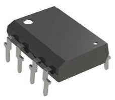
74HC132 Trigger: Circuit, Pinout, and Datasheet

Toshiba Semiconductor and Storage
8.65mm mm Gates & Inverters 2V~6V V
Unit Price: $0.330482
Ext Price: $0.33


8.65mm mm Gates & Inverters 2V~6V V
The 74HC132 is a silicon gate C²MOS-fabricated high-speed CMOS 2-INPUT NAND SCHMITT TRIGGER GATE. This article mainly introduces circuit, pinout, datasheet and other detailed information about Toshiba Semiconductor and Storage 74HC132.

7410 74HC10 Triple 3 input NAND gate integrated circuit IC demonstration by electronzap electronics
74HC132 Description
The 74HC132 is a silicon gate C²MOS-fabricated high-speed CMOS 2-INPUT NAND SCHMITT TRIGGER GATE. It achieves high-speed operation comparable to LSTTL while keeping CMOS low power dissipation.
The 74HC132 has the same pin arrangement and function as the 74HC00D, but the inputs have a 25% VCC hysteresis and may be used as a line receiver for sluggish input signals thanks to its schmitt trigger inputs.
Static discharge and transient excess voltage safety circuits are installed on all inputs.
74HC132 Pinout

Pinout
| Pin Number | Pin Name | Description |
| 1 | 1A | Channel 1, Input A |
| 2 | 1B | Channel 1, Input B |
| 3 | 1Y | Channel 1, Output Y |
| 4 | 2A | Channel 2, Input A |
| 5 | 2B | Channel 2, Input B |
| 6 | 2Y | Channel 2, Output Y |
| 7 | GND | Ground |
| 8 | 3Y | Channel 3, Output Y |
| 9 | 3A | Channel 3, Input A |
| 10 | 3B | Channel 3, Input B |
| 11 | 4Y | Channel 4, Output Y |
| 12 | 4A | Channel 4, Input A |
| 13 | 4B | Channel 4, Input B |
| 14 | VCC | Positive Supply |
74HC132 CAD Model

Symbol

Footprint

3D Model
74HC132 Features
• High speed: tpd = 11 ns (typ.) at VCC = 5 V
• Low power dissipation: ICC = 1.0 µA (max) at Ta = 25°C
• High noise immunity: VH = 1.1 V (typ.) at VCC = 4.5 V
• Balanced propagation delays: tPLH ≈ tPHL
• Wide operating voltage range: VCC(opr) = 2.0 to 6.0 V
• Unlimited input rise and fall times
• Latch-up performance exceeds 100 mA per JESD 78 Class II Level B
• Complies with JEDEC standards:
- JESD8C (2.7 V to 3.6 V)
- JESD7A (2.0 V to 6.0 V)
• ESD protection:
- HBM JESD22-A114F exceeds 2000 V
- MM JESD22-A115-A exceeds 200 V
• Multiple package options
• Specified from −40 °C to +85 °C and from −40 °C to +125 °C
Specifications
- TypeParameter
- Factory Lead Time12 Weeks
- Mounting Type
The "Mounting Type" in electronic components refers to the method used to attach or connect a component to a circuit board or other substrate, such as through-hole, surface-mount, or panel mount.
Surface Mount - Package / Case
refers to the protective housing that encases an electronic component, providing mechanical support, electrical connections, and thermal management.
14-SOIC (0.154, 3.90mm Width) - Surface Mount
having leads that are designed to be soldered on the side of a circuit board that the body of the component is mounted on.
YES - Usage LevelIndustrial grade
- Operating Temperature
The operating temperature is the range of ambient temperature within which a power supply, or any other electrical equipment, operate in. This ranges from a minimum operating temperature, to a peak or maximum operating temperature, outside which, the power supply may fail.
-40°C~85°C - Packaging
Semiconductor package is a carrier / shell used to contain and cover one or more semiconductor components or integrated circuits. The material of the shell can be metal, plastic, glass or ceramic.
Cut Tape (CT) - Series
In electronic components, the "Series" refers to a group of products that share similar characteristics, designs, or functionalities, often produced by the same manufacturer. These components within a series typically have common specifications but may vary in terms of voltage, power, or packaging to meet different application needs. The series name helps identify and differentiate between various product lines within a manufacturer's catalog.
74HC - Published2016
- Part Status
Parts can have many statuses as they progress through the configuration, analysis, review, and approval stages.
Active - Moisture Sensitivity Level (MSL)
Moisture Sensitivity Level (MSL) is a standardized rating that indicates the susceptibility of electronic components, particularly semiconductors, to moisture-induced damage during storage and the soldering process, defining the allowable exposure time to ambient conditions before they require special handling or baking to prevent failures
1 (Unlimited) - Number of Terminations14
- Voltage - Supply
Voltage - Supply refers to the range of voltage levels that an electronic component or circuit is designed to operate with. It indicates the minimum and maximum supply voltage that can be applied for the device to function properly. Providing supply voltages outside this range can lead to malfunction, damage, or reduced performance. This parameter is critical for ensuring compatibility between different components in a circuit.
2V~6V - Terminal Position
In electronic components, the term "Terminal Position" refers to the physical location of the connection points on the component where external electrical connections can be made. These connection points, known as terminals, are typically used to attach wires, leads, or other components to the main body of the electronic component. The terminal position is important for ensuring proper connectivity and functionality of the component within a circuit. It is often specified in technical datasheets or component specifications to help designers and engineers understand how to properly integrate the component into their circuit designs.
DUAL - Terminal Form
Occurring at or forming the end of a series, succession, or the like; closing; concluding.
GULL WING - Peak Reflow Temperature (Cel)
Peak Reflow Temperature (Cel) is a parameter that specifies the maximum temperature at which an electronic component can be exposed during the reflow soldering process. Reflow soldering is a common method used to attach electronic components to a circuit board. The Peak Reflow Temperature is crucial because it ensures that the component is not damaged or degraded during the soldering process. Exceeding the specified Peak Reflow Temperature can lead to issues such as component failure, reduced performance, or even permanent damage to the component. It is important for manufacturers and assemblers to adhere to the recommended Peak Reflow Temperature to ensure the reliability and functionality of the electronic components.
NOT SPECIFIED - Number of Functions4
- Supply Voltage
Supply voltage refers to the electrical potential difference provided to an electronic component or circuit. It is crucial for the proper operation of devices, as it powers their functions and determines performance characteristics. The supply voltage must be within specified limits to ensure reliability and prevent damage to components. Different electronic devices have specific supply voltage requirements, which can vary widely depending on their design and intended application.
5V - Time@Peak Reflow Temperature-Max (s)
Time@Peak Reflow Temperature-Max (s) refers to the maximum duration that an electronic component can be exposed to the peak reflow temperature during the soldering process, which is crucial for ensuring reliable solder joint formation without damaging the component.
NOT SPECIFIED - Supply Voltage-Max (Vsup)
The parameter "Supply Voltage-Max (Vsup)" in electronic components refers to the maximum voltage that can be safely applied to the component without causing damage. It is an important specification to consider when designing or using electronic circuits to ensure the component operates within its safe operating limits. Exceeding the maximum supply voltage can lead to overheating, component failure, or even permanent damage. It is crucial to adhere to the specified maximum supply voltage to ensure the reliable and safe operation of the electronic component.
6V - Supply Voltage-Min (Vsup)
The parameter "Supply Voltage-Min (Vsup)" in electronic components refers to the minimum voltage level required for the component to operate within its specified performance range. This parameter indicates the lowest voltage that can be safely applied to the component without risking damage or malfunction. It is crucial to ensure that the supply voltage provided to the component meets or exceeds this minimum value to ensure proper functionality and reliability. Failure to adhere to the specified minimum supply voltage may result in erratic behavior, reduced performance, or even permanent damage to the component.
2V - Number of Circuits4
- Family
In electronic components, the parameter "Family" typically refers to a categorization or classification system used to group similar components together based on their characteristics, functions, or applications. This classification helps users easily identify and select components that meet their specific requirements. The "Family" parameter can include various subcategories such as resistors, capacitors, diodes, transistors, integrated circuits, and more. Understanding the "Family" of an electronic component can provide valuable information about its compatibility, performance specifications, and potential uses within a circuit or system. It is important to consider the "Family" parameter when designing or troubleshooting electronic circuits to ensure proper functionality and compatibility with other components.
HC/UH - Number of Inputs2
- Logic Type
Logic Type in electronic components refers to the classification of circuits based on the logical operations they perform. It includes types such as AND, OR, NOT, NAND, NOR, XOR, and XNOR, each defining the relationship between binary inputs and outputs. The logic type determines how the inputs affect the output state based on specific rules of Boolean algebra. This classification is crucial for designing digital circuits and systems, enabling engineers to select appropriate components for desired functionalities.
NAND Gate - Max Propagation Delay @ V, Max CL
The parameter "Max Propagation Delay @ V, Max CL" in electronic components refers to the maximum amount of time it takes for a signal to propagate through the component from input to output when operating at a specific voltage (V) and driving a maximum specified load capacitance (CL). This parameter is crucial in determining the speed and performance of the component in a circuit. A shorter propagation delay indicates faster signal processing and better overall performance. Designers use this parameter to ensure that signals can be transmitted and received within the required timing constraints in their electronic systems.
19ns @ 5V, 50pF - Current - Quiescent (Max)
The parameter "Current - Quiescent (Max)" in electronic components refers to the maximum amount of current that a device consumes when it is in a quiescent or idle state. This parameter is important because it indicates the minimum power consumption of the device when it is not actively performing any tasks. It is typically measured in units of amperes (A) and helps in determining the overall power efficiency and battery life of the electronic component. Designers and engineers use this parameter to ensure that the device meets power consumption requirements and operates within specified limits during standby or idle modes.
1μA - Features
In the context of electronic components, the term "Features" typically refers to the specific characteristics or functionalities that a particular component offers. These features can vary depending on the type of component and its intended use. For example, a microcontroller may have features such as built-in memory, analog-to-digital converters, and communication interfaces like UART or SPI.When evaluating electronic components, understanding their features is crucial in determining whether they meet the requirements of a particular project or application. Engineers and designers often look at features such as operating voltage, speed, power consumption, and communication protocols to ensure compatibility and optimal performance.In summary, the "Features" parameter in electronic components describes the unique attributes and capabilities that differentiate one component from another, helping users make informed decisions when selecting components for their electronic designs.
Schmitt Trigger - Length8.65mm
- Height Seated (Max)
Height Seated (Max) is a parameter in electronic components that refers to the maximum allowable height of the component when it is properly seated or installed on a circuit board or within an enclosure. This specification is crucial for ensuring proper fit and alignment within the overall system design. Exceeding the maximum seated height can lead to mechanical interference, electrical shorts, or other issues that may impact the performance and reliability of the electronic device. Manufacturers provide this information to help designers and engineers select components that will fit within the designated space and function correctly in the intended application.
1.75mm - Width3.9mm
- RoHS Status
RoHS means “Restriction of Certain Hazardous Substances” in the “Hazardous Substances Directive” in electrical and electronic equipment.
RoHS Compliant
74HC132 Voltage Doubler Circuit
Using the electronic design below, you may construct a voltage doubler circuit. This electrical circuit, which uses the 74HC132 or 74HCT132 circuit type, has a very cheap manufacturing cost. Only four components, C4, C5, D1, and D2, are required to produce a voltage of 10 V to 5 V when the CLK signal is sent through the buffer. Two additional components, R1 and C3, are necessary if the power oscillator is to be created from an unused gate.
The table below lists the most crucial circuit parameters.

Circuit Diagram
74HC132 Alternatives
| Part Number | Description | Manufacturer |
| 74HC132PWLOGIC | NAND Gate, HC/UH Series, 4-Func, 2-Input, CMOS, PDSO14 | Nexperia |
| 74HC132PW-TLOGIC | IC HC/UH SERIES, QUAD 2-INPUT NAND GATE, PDSO14, SOT-402-1, TSSOP-14, Gate | NXP Semiconductors |
| MC74HC132ADTR2GLOGIC | Quad 2-Input NAND Gate with Schmitt Trigger Input, TSSOP-14, 2500-REEL | onsemi |
74HC132 Applications
74HC132 Package

Package
74HC132 Manufacturer
Toshiba Semiconductor & Storage provides a wide range of supporting technology solutions that enable OEMs, ODMs, CMs, and fabless semiconductor businesses to create innovative integrated products for industries such as computers, networking, communications, digital consumer, automotive, and others.
Trend Analysis
Parts with Similar Specs
1.What chip is 74HC132?
74HC132 is a quad 2 input terminal and non-Schmitt trigger, CMOS device, power supply operating voltage 2V ~ 6V.
2.If the motherboard power-on circuit is broken, what type of replacement should be used for 74HC132?
74HC132 is a four 2-input NAND gate (Schmidt input). Which model can be used instead depends on the specific circuit.
For example, if all the logic devices in the original circuit are TTL circuits, 74HCT132D can also be used. If the operating voltage of the original circuit is in the range of 2V~5.5V, 74AHC132D can also be used. There are also many Schmidt input NAND gates with slight differences in operating voltage and speed. The pins are compatible with 74HC132, such as 74VHC132, 74AC132, 74LVX132, etc. Even 74HC00 is not absolutely irreplaceable. 74HC132 is also pin-compatible, the only difference is that it is not Schmidt input. So everything depends on the specific conditions of the actual circuit.
3.What is the role of 74HC132?
74HC132 is four 2-input terminals with non-Schmitt triggers. The function is the NAND operation of 2 inputs, which must meet the NAND operation under the input and output conditions of the Schmitt trigger.
 D880 NPN Transistor: Datasheet, Pinout and Equivalent
25 October 202111097
 ATTINY13 8-bit AVR Microcontroller: Pinout, Equivalent and Datasheet
16 December 20214113
 AV101KE Through Hole Resistor: Datasheet, Application, Features
30 July 2021936
 1PS79SB30 Single Diode: Schottky, 40V, 200mA, Datasheet PDF
28 February 2022752
 Transistor PN2222A Silicon NPN Audio Amplifier: Pinout, Datasheet, and Package
12 January 20223956
 AD823 Op-Amp Troubleshooting Guide: Common Failures and Repair Solutions
04 July 2025588
 TLP250 Photocoupler: Schematic, Pinout and Datasheet
11 September 202116511
 TXS0102DCUR Translator: Features, Applications and Datasheet
11 November 2023413
 Dismantling and Analyzing Each Component in the Switching Power Supply
16 February 20227973
 What is Chiplet?
17 November 20213793
 A User Guide to Automotive Relay
30 July 20216817
 The Future of Automated and Additive Manufacturing for Power Electronics
24 May 20233079
 BMW CEO: The Car Chip Problem Will Not Be Solved Until 2023
12 April 20225246
 All About Video Connectors and Their Uses in Today’s Technology
02 July 20252579
 What is Surge?
09 February 20226185
 Weak Current Control Strong Current: How to use the Relay?
28 November 20225722
Toshiba Semiconductor and Storage
In Stock: 21000
Minimum: 1 Multiples: 1
Qty
Unit Price
Ext Price
1
$0.330482
$0.33
10
$0.311775
$3.12
100
$0.294128
$29.41
500
$0.277479
$138.74
1000
$0.261773
$261.77
Not the price you want? Send RFQ Now and we'll contact you ASAP.
Inquire for More Quantity
![74VHC00FT]() 74VHC00FT
74VHC00FTToshiba Semiconductor and Storage
![74VHCT00AFT]() 74VHCT00AFT
74VHCT00AFTToshiba Semiconductor and Storage
![TC74HC00AP]() TC74HC00AP
TC74HC00APToshiba
![TC74HC04AP]() TC74HC04AP
TC74HC04APToshiba
![74VHC32FT]() 74VHC32FT
74VHC32FTToshiba Semiconductor and Storage
![TC4011BP]() TC4011BP
TC4011BPToshiba
![74VHC04FT]() 74VHC04FT
74VHC04FTToshiba Semiconductor and Storage
![TC74HC08AP]() TC74HC08AP
TC74HC08APToshiba
![TC4S584F(TE85L)]() TC4S584F(TE85L)
TC4S584F(TE85L)Toshiba
![74LCX14FT]() 74LCX14FT
74LCX14FTToshiba Semiconductor and Storage

