

 Product
 Brand
Brand Articles
 Tools
Tools
ADG1204 Multiplexer: Pinout, Features and Datasheet

85ns, 110ns SP4T 190Ohm QUAD Analog Switches BREAK-BEFORE-MAKE ADG1204 100pA 12-WFQFN Exposed Pad, CSP


85ns, 110ns SP4T 190Ohm QUAD Analog Switches BREAK-BEFORE-MAKE ADG1204 100pA 12-WFQFN Exposed Pad, CSP
The ADG1204 is a complementary metal-oxide semiconductor (CMOS) analog multiplexer, comprising four single channels designed on an iCMOS (industrial CMOS) process. Furthermore, Huge range of Semiconductors, Capacitors, Resistors and IcS in stock. Welcome RFQ.

Multiplexers and DeMultiplexers
ADG1204 Pinout
The following figure is the diagram of ADG1204 pinout.

Pinout
ADG1204 CAD Model
The followings are ADG1204 Symbol, Footprint.
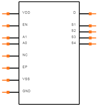
Symbol

Footprint
ADG1204 Overview
The ADG1204 is a complementary metal-oxide semiconductor (CMOS) analog multiplexer, comprising four single channels designed on an iCMOS (industrial CMOS) process. iCMOS® is a modular manufacturing process that combines high voltage CMOS and bipolar technologies. It enables the development of a wide range of high performance analog ICs capable of 33 V operation in a footprint that no previous generation of high voltage devices has been able to achieve. Unlike analog ICs using conventional CMOS processes, iCMOS components can tolerate high supply voltages while providing increased performance, dramatically lower power consumption, and reduced package size. The ADG1204 switches one of four inputs to a common output, D, as determined by the 3-bit binary address lines: A0, A1, and EN. Logic 0 on the EN pin disables the device. Each switch conducts equally well in both directions when on and has an input signal range that extends to the supplies. In the off condition, signal levels up to the supplies are blocked. All switches exhibit breakbefore-make switching action.
This article provides you with a basic overview of the ADG1204 Multiplexer, including its pin descriptions, features and specifications, etc., to help you quickly understand what ADG1204 is.
ADG1204 Features
● 1.5 pF off source capacitance
● <1 pC charge injection
● 33 V supply range
● 120 Ω on resistance
● Fully specified at ±15 V, +12 V
● No VL supply required
● 3 V logic-compatible inputs
● Rail-to-rail operation
● 14-lead TSSOP and 12-lead LFCSP
● Typical power consumption < 0.03 μW
ADG1204 Product Highlights
● 1.5 pF off capacitance (±15 V supply).
● <1 pC charge injection.
● 3 V logic-compatible digital inputs: VIH = 2.0 V, VIL = 0.8 V.
● No VL logic power supply required.
● Ultralow power dissipation: <0.03 μW.
● 14-lead TSSOP and 12-lead, 3 mm × 3 mm LFCSP packages.
Specifications
- TypeParameter
- Lifecycle Status
Lifecycle Status refers to the current stage of an electronic component in its product life cycle, indicating whether it is active, obsolete, or transitioning between these states. An active status means the component is in production and available for purchase. An obsolete status indicates that the component is no longer being manufactured or supported, and manufacturers typically provide a limited time frame for support. Understanding the lifecycle status is crucial for design engineers to ensure continuity and reliability in their projects.
PRODUCTION (Last Updated: 1 month ago) - Factory Lead Time8 Weeks
- Contact Plating
Contact plating (finish) provides corrosion protection for base metals and optimizes the mechanical and electrical properties of the contact interfaces.
Tin - Mounting Type
The "Mounting Type" in electronic components refers to the method used to attach or connect a component to a circuit board or other substrate, such as through-hole, surface-mount, or panel mount.
Surface Mount - Package / Case
refers to the protective housing that encases an electronic component, providing mechanical support, electrical connections, and thermal management.
12-WFQFN Exposed Pad, CSP - Surface Mount
having leads that are designed to be soldered on the side of a circuit board that the body of the component is mounted on.
YES - Number of Pins12
- Current - Supply (Nom)250μA
- Turn Off Delay Time
It is the time from when Vgs drops below 90% of the gate drive voltage to when the drain current drops below 90% of the load current. It is the delay before current starts to transition in the load, and depends on Rg. Ciss.
90 ns - Operating Temperature
The operating temperature is the range of ambient temperature within which a power supply, or any other electrical equipment, operate in. This ranges from a minimum operating temperature, to a peak or maximum operating temperature, outside which, the power supply may fail.
-40°C~125°C TA - Packaging
Semiconductor package is a carrier / shell used to contain and cover one or more semiconductor components or integrated circuits. The material of the shell can be metal, plastic, glass or ceramic.
Tape & Reel (TR) - JESD-609 Code
The "JESD-609 Code" in electronic components refers to a standardized marking code that indicates the lead-free solder composition and finish of electronic components for compliance with environmental regulations.
e3 - Pbfree Code
The "Pbfree Code" parameter in electronic components refers to the code or marking used to indicate that the component is lead-free. Lead (Pb) is a toxic substance that has been widely used in electronic components for many years, but due to environmental concerns, there has been a shift towards lead-free alternatives. The Pbfree Code helps manufacturers and users easily identify components that do not contain lead, ensuring compliance with regulations and promoting environmentally friendly practices. It is important to pay attention to the Pbfree Code when selecting electronic components to ensure they meet the necessary requirements for lead-free applications.
no - Part Status
Parts can have many statuses as they progress through the configuration, analysis, review, and approval stages.
Active - Moisture Sensitivity Level (MSL)
Moisture Sensitivity Level (MSL) is a standardized rating that indicates the susceptibility of electronic components, particularly semiconductors, to moisture-induced damage during storage and the soldering process, defining the allowable exposure time to ambient conditions before they require special handling or baking to prevent failures
3 (168 Hours) - Number of Terminations12
- ECCN Code
An ECCN (Export Control Classification Number) is an alphanumeric code used by the U.S. Bureau of Industry and Security to identify and categorize electronic components and other dual-use items that may require an export license based on their technical characteristics and potential for military use.
EAR99 - Resistance
Resistance is a fundamental property of electronic components that measures their opposition to the flow of electric current. It is denoted by the symbol "R" and is measured in ohms (Ω). Resistance is caused by the collisions of electrons with atoms in a material, which generates heat and reduces the flow of current. Components with higher resistance will impede the flow of current more than those with lower resistance. Resistance plays a crucial role in determining the behavior and functionality of electronic circuits, such as limiting current flow, voltage division, and controlling power dissipation.
190Ohm - Max Power Dissipation
The maximum power that the MOSFET can dissipate continuously under the specified thermal conditions.
1.3mW - Voltage - Supply
Voltage - Supply refers to the range of voltage levels that an electronic component or circuit is designed to operate with. It indicates the minimum and maximum supply voltage that can be applied for the device to function properly. Providing supply voltages outside this range can lead to malfunction, damage, or reduced performance. This parameter is critical for ensuring compatibility between different components in a circuit.
15V - Terminal Position
In electronic components, the term "Terminal Position" refers to the physical location of the connection points on the component where external electrical connections can be made. These connection points, known as terminals, are typically used to attach wires, leads, or other components to the main body of the electronic component. The terminal position is important for ensuring proper connectivity and functionality of the component within a circuit. It is often specified in technical datasheets or component specifications to help designers and engineers understand how to properly integrate the component into their circuit designs.
QUAD - Peak Reflow Temperature (Cel)
Peak Reflow Temperature (Cel) is a parameter that specifies the maximum temperature at which an electronic component can be exposed during the reflow soldering process. Reflow soldering is a common method used to attach electronic components to a circuit board. The Peak Reflow Temperature is crucial because it ensures that the component is not damaged or degraded during the soldering process. Exceeding the specified Peak Reflow Temperature can lead to issues such as component failure, reduced performance, or even permanent damage to the component. It is important for manufacturers and assemblers to adhere to the recommended Peak Reflow Temperature to ensure the reliability and functionality of the electronic components.
260 - Number of Functions1
- Terminal Pitch
The center distance from one pole to the next.
0.5mm - Time@Peak Reflow Temperature-Max (s)
Time@Peak Reflow Temperature-Max (s) refers to the maximum duration that an electronic component can be exposed to the peak reflow temperature during the soldering process, which is crucial for ensuring reliable solder joint formation without damaging the component.
40 - Base Part Number
The "Base Part Number" (BPN) in electronic components serves a similar purpose to the "Base Product Number." It refers to the primary identifier for a component that captures the essential characteristics shared by a group of similar components. The BPN provides a fundamental way to reference a family or series of components without specifying all the variations and specific details.
ADG1204 - Operating Supply Voltage
The voltage level by which an electrical system is designated and to which certain operating characteristics of the system are related.
12V - Number of Channels4
- Interface
In electronic components, the term "Interface" refers to the point at which two different systems, devices, or components connect and interact with each other. It can involve physical connections such as ports, connectors, or cables, as well as communication protocols and standards that facilitate the exchange of data or signals between the connected entities. The interface serves as a bridge that enables seamless communication and interoperability between different parts of a system or between different systems altogether. Designing a reliable and efficient interface is crucial in ensuring proper functionality and performance of electronic components and systems.
Parallel - Number of Circuits1
- Analog IC - Other Type
Analog IC - Other Type is a parameter used to categorize electronic components that are integrated circuits (ICs) designed for analog signal processing but do not fall into more specific subcategories such as amplifiers, comparators, or voltage regulators. These ICs may include specialized analog functions such as analog-to-digital converters (ADCs), digital-to-analog converters (DACs), voltage references, or signal conditioning circuits. They are typically used in various applications where precise analog signal processing is required, such as in audio equipment, instrumentation, communication systems, and industrial control systems. Manufacturers provide detailed specifications for these components to help engineers select the most suitable IC for their specific design requirements.
SINGLE-ENDED MULTIPLEXER - Power Dissipation
the process by which an electronic or electrical device produces heat (energy loss or waste) as an undesirable derivative of its primary action.
1.3mW - Number of Bits4
- Throw Configuration
"Throw Configuration" is a term commonly used in the context of switches and relays in electronic components. It refers to the number of positions or states that the switch or relay can be set to. For example, a single-throw (ST) configuration means the switch has only one position, while a double-throw (DT) configuration means the switch has two positions.The throw configuration is important because it determines the versatility and functionality of the switch or relay. Different applications may require different throw configurations to control the flow of current or signals effectively. Understanding the throw configuration of a component is crucial for proper installation and operation within an electronic circuit.
4PST - Current - Supply
Current - Supply is a parameter in electronic components that refers to the maximum amount of electrical current that the component can provide to the circuit it is connected to. It is typically measured in units of amperes (A) and is crucial for determining the power handling capability of the component. Understanding the current supply rating is important for ensuring that the component can safely deliver the required current without overheating or failing. It is essential to consider this parameter when designing circuits to prevent damage to the component and ensure proper functionality of the overall system.
250μA - Supply Current-Max (Isup)
Supply Current-Max (Isup) refers to the maximum amount of current that an electronic component can draw from its power supply during operation. It represents the peak current demand of the device under normal operating conditions and is critical for ensuring that the power supply can adequately support the component's needs without risking damage or malfunction. This parameter is essential for designing circuits and selecting appropriate power supply units to prevent overloading and ensure reliable performance.
0.23mA - Neg Supply Voltage-Nom (Vsup)
The parameter "Neg Supply Voltage-Nom (Vsup)" in electronic components refers to the nominal negative supply voltage that the component requires to operate within its specified performance characteristics. This parameter indicates the minimum voltage level that must be provided to the component's negative supply pin for proper functionality. It is important to ensure that the negative supply voltage provided to the component does not exceed the maximum specified value to prevent damage or malfunction. Understanding and adhering to the specified negative supply voltage requirements is crucial for the reliable operation of the electronic component in a circuit.
-15V - On-State Resistance (Max)
The "On-State Resistance (Max)" parameter in electronic components refers to the maximum resistance exhibited by the component when it is in the fully conducting state. This resistance is typically measured when the component is carrying the maximum specified current. A lower on-state resistance indicates better conductivity and efficiency of the component when it is in the on-state. It is an important parameter to consider when selecting components for applications where low power dissipation and high efficiency are critical factors.
190Ohm - High Level Output Current
High-level Output Current IOH The current flowing into the output at a specified high- level voltage. Low-level Output Current IOL The current flowing into the output at a specified low- level output voltage.
45mA - Dual Supply Voltage
Dual Supply Voltage refers to an electronic component's requirement for two separate power supply voltages, typically one positive and one negative. This configuration is commonly used in operational amplifiers, analog circuits, and certain digital devices to allow for greater signal handling capabilities and improved performance. The use of dual supply voltages enables the device to process bipolar signals, thereby enhancing its functionality in various applications.
15V - Multiplexer/Demultiplexer Circuit
A Multiplexer/Demultiplexer Circuit is an electronic component used in digital circuits to select one of several input signals and route it to a single output. A multiplexer, also known as a "mux," is used to combine multiple input signals into a single output, while a demultiplexer, also known as a "demux," is used to take a single input and route it to one of several possible outputs. These circuits are commonly used in data transmission, communication systems, and digital signal processing applications to efficiently manage and control the flow of data. Multiplexers and demultiplexers play a crucial role in optimizing the use of resources and improving the overall performance of electronic systems.
4:1 - Off-state Isolation-Nom
Off-state Isolation-Nom is a parameter used to measure the level of isolation between two electronic components or circuits when one of them is in the off state. It indicates the ability of the component to prevent unwanted signals or interference from passing through when it is not actively conducting. The parameter is typically expressed in decibels (dB) and is an important consideration in designing and selecting components for applications where isolation between different parts of a circuit is critical to prevent crosstalk or interference. Higher values of Off-state Isolation-Nom indicate better isolation performance, leading to improved overall system reliability and performance.
85 dB - Current - Leakage (IS(off)) (Max)
Current - Leakage (IS(off)) (Max) refers to the maximum amount of current that flows through a device when it is in its off state, meaning it is not conducting or not intended to be active. This parameter is crucial in determining the efficiency of electronic components, especially in battery-operated devices, as higher leakage currents can lead to increased power consumption and reduced battery life. It is typically measured in microamperes (µA) or milliamperes (mA) and helps engineers assess the suitability of a component for low-power applications.
100pA - Channel Capacitance (CS(off), CD(off))
Channel capacitance (CS(off), CD(off)) in electronic components refers to the capacitance associated with the channel of a field-effect transistor (FET) when it is turned off. CS(off) represents the capacitance between the source and the gate of the FET, while CD(off) represents the capacitance between the drain and the gate. These capacitances play a crucial role in determining the high-frequency performance and switching characteristics of the FET. Understanding and controlling these capacitances is essential for optimizing the performance of electronic circuits, especially in high-speed applications where minimizing parasitic capacitances is critical for achieving desired signal integrity and efficiency.
1.5pF 4.2pF - On-state Resistance Match-Nom
On-state Resistance Match-Nom refers to the nominal or standard value of the on-state resistance for a specific electronic component, such as a transistor or a MOSFET, when it is in its "on" state. This parameter indicates how much resistance the component presents to current flow during its conducting phase, which affects power dissipation and efficiency. Matching this value across multiple devices is crucial for ensuring consistent performance in applications where several components operate together.
3.5Ohm - Switch Circuit
establishes connections between links, on demand and as available, in order to establish an end-to-end circuit between devices.
SP4T - Switch Time (Ton, Toff) (Max)
The parameter "Switch Time (Ton, Toff) (Max)" in electronic components refers to the maximum time it takes for a device to transition between its on and off states. Ton represents the turn-on time, which is the time taken for the device to switch from the off state to the on state, while Toff represents the turn-off time, which is the time taken for the device to switch from the on state to the off state. This parameter is crucial in determining the speed and efficiency of the device's switching operation. A shorter switch time generally indicates faster switching speeds and better performance of the electronic component.
85ns, 110ns - Charge Injection
A Charge injection in analog switches and multiplexers is a level change caused by stray capacitance associated with the NMOS and PMOS transistors that make up the analog switch.
-0.7pC - Channel-to-Channel Matching (ΔRon)
Channel-to-Channel Matching (ΔRon) refers to the variation in the on-resistance of multiple channels within a multi-channel electronic component, such as a multiplexer or a switch. It is a measure of how closely the on-resistance values of different channels match each other. The lower the ΔRon value, the better the matching between channels, which is important for ensuring consistent performance across all channels in a system. Channel-to-Channel Matching is critical in applications where precise and uniform signal processing is required, such as in instrumentation, audio equipment, and communication systems. Manufacturers provide specifications for ΔRon to help designers select components that meet their performance requirements.
6 Ω - Switching
In electronic components, "Switching" refers to the process of turning a device on or off, or changing its state from one condition to another. This parameter is crucial in determining the speed and efficiency of a component's operation. It is often measured in terms of switching time, which is the time taken for a device to transition from one state to another. The switching characteristics of a component play a significant role in its overall performance and reliability in electronic circuits.
BREAK-BEFORE-MAKE - Switch-on Time-Max
Switch-on Time-Max is a parameter in electronic components that refers to the maximum time it takes for a device to turn on completely after receiving a signal or command. This parameter is crucial in determining the responsiveness and efficiency of the component in various applications. A shorter switch-on time-max indicates a faster response time, which is important in applications where quick activation is required. Manufacturers provide this specification to help users understand the performance characteristics of the component and ensure it meets the requirements of their specific application.
85ns - Drain to Source Resistance
The Drain to Source Resistance, often denoted as RDS(on), is a crucial parameter in electronic components, particularly in field-effect transistors (FETs) such as MOSFETs. It represents the resistance between the drain and source terminals when the FET is in its on-state, conducting current. A lower RDS(on) value indicates better conductivity and efficiency, as it results in less power dissipation and heat generation in the component. Designers often aim to minimize RDS(on) to improve the performance and overall efficiency of electronic circuits, especially in power applications where minimizing losses is critical.
190Ohm - Voltage - Supply, Dual (V±)
The parameter "Voltage - Supply, Dual (V±)" refers to the range of dual supply voltages required for the operation of an electronic component. This specification indicates that the component can operate with both positive and negative voltage levels, typically represented as V+ for the positive voltage and V- for the negative voltage. It is commonly used in analog devices and operational amplifiers to facilitate signal processing that requires a reference point at ground level, allowing for both upwards and downwards signal variations. A typical example would be V+ = +15V and V- = -15V, indicating the component can operate effectively within that voltage range.
±15V - Height950μm
- Length3.15mm
- Width2.95mm
- REACH SVHC
The parameter "REACH SVHC" in electronic components refers to the compliance with the Registration, Evaluation, Authorization, and Restriction of Chemicals (REACH) regulation regarding Substances of Very High Concern (SVHC). SVHCs are substances that may have serious effects on human health or the environment, and their use is regulated under REACH to ensure their safe handling and minimize their impact.Manufacturers of electronic components need to declare if their products contain any SVHCs above a certain threshold concentration and provide information on the safe use of these substances. This information allows customers to make informed decisions about the potential risks associated with using the components and take appropriate measures to mitigate any hazards.Ensuring compliance with REACH SVHC requirements is essential for electronics manufacturers to meet regulatory standards, protect human health and the environment, and maintain transparency in their supply chain. It also demonstrates a commitment to sustainability and responsible manufacturing practices in the electronics industry.
No SVHC - Radiation Hardening
Radiation hardening is the process of making electronic components and circuits resistant to damage or malfunction caused by high levels of ionizing radiation, especially for environments in outer space (especially beyond the low Earth orbit), around nuclear reactors and particle accelerators, or during nuclear accidents or nuclear warfare.
No - RoHS Status
RoHS means “Restriction of Certain Hazardous Substances” in the “Hazardous Substances Directive” in electrical and electronic equipment.
ROHS3 Compliant - Lead Free
Lead Free is a term used to describe electronic components that do not contain lead as part of their composition. Lead is a toxic material that can have harmful effects on human health and the environment, so the electronics industry has been moving towards lead-free components to reduce these risks. Lead-free components are typically made using alternative materials such as silver, copper, and tin. Manufacturers must comply with regulations such as the Restriction of Hazardous Substances (RoHS) directive to ensure that their products are lead-free and environmentally friendly.
Contains Lead
ADG1204 Functional Block Diagram
The following is the Functional Block Diagram of ADG1204.
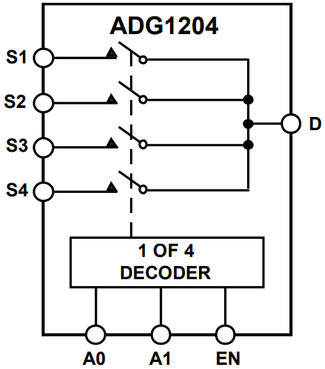
Functional Block Diagram
ADG1204 Equivalent
| Model number | Manufacturer | Description |
| ADG1204YCPZ-REEL7 | Analog Devices Inc | Low Capacitance, Low Charge Injection, ±15 V/+12 V, 4:1 iCMOS Multiplexer |
ADG1204 Applications
● Automatic test equipment
● Data acquisition systems
● Battery-powered systems
● Sample-and-hold systems
● Audio signal routing
● Video signal routing
● Communication systems
ADG1204 Package
The following diagram shows the ADG1204 package.
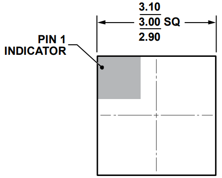
Top View
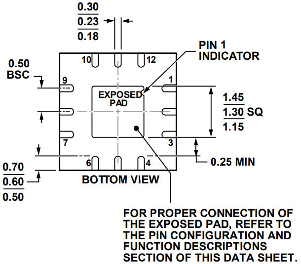
Bottom View
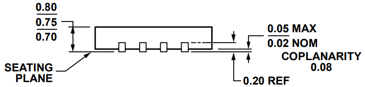
Side View
ADG1204 Manufacturer
Analog Devices (NASDAQ: ADI) is a world leader in the design, manufacture, and marketing of a broad portfolio of high performance analog, mixed-signal, and digital signal processing (DSP) integrated circuits (ICs) used in virtually all types of electronic equipment. Since our inception in 1965, we have focused on solving the engineering challenges associated with signal processing in electronic equipment. Used by over 100,000 customers worldwide, our signal processing products play a fundamental role in converting, conditioning, and processing real-world phenomena such as temperature, pressure, sound, light, speed, and motion into electrical signals to be used in a wide array of electronic devices.
Trend Analysis
Datasheet PDF
- Datasheets :
- PCN Other :
- ConflictMineralStatement :
What is the essential property of the ADG1204?
The ADG1204 is a complementary metal-oxide semiconductor (CMOS) analog multiplexer, comprising four single channels designed on an iCMOS (industrial CMOS) process.
What makes the ADG1204 multiplexer an ideal solution for data acquisition and sample-andhold applications?
The ultralow capacitance and charge injection of this multiplexer makes it an ideal solution for data acquisition and sample-andhold applications, where low glitch and fast settling are required.
![LM2901D Analog Comparator Overview [Video]](https://res.utmel.com/Images/Article/8ab44ea1-170a-4539-a73d-5ee8c487aac2.png) LM2901D Analog Comparator Overview [Video]
LM2901D Analog Comparator Overview [Video]14 August 20241703
 TLV70033DDCR: Low Quiescent, Pinout, Datasheet
09 March 20222416
 AD708 Dual Precision Op Amp: DC Performance Analysis and Modern Replacement Notes
20 May 2026414
 LT1054 Voltage Converter and Regulator: Pinout, Applications and Datasheet
03 November 20214861
 Advantech Corp 96MPXE-2.1-16M36: A Discontinued Skylake Microprocessor Module
11 March 20243709
 STM32F051C8T6 Microcontroller: Features, Applications and Datasheet
08 December 2023957
 D44H8 Power Transistor: Pinout, Datasheet, and Applications
21 July 20211402
 STM32G030K6T6 Microcontrollers: Features, Applications and Datasheet
20 December 20233881
 What is Feedthrough Capacitor?
06 November 202142088
 What is PWM "Dead Band"?
21 April 20228359
 Role of Direct Memory Access in Modern Computing
12 November 20246631
 The Introduction of Car Fuse
09 October 20217132
 Flyback Diode Relay Selection: How to Choose the Right Diode for a Relay Coil
11 June 20263297
 Silicon Carbide Substrate Manufacturing: Advancing Technology to New Heights
08 June 20233895
 Best 1N4007 diode alternatives to use in 2025
25 August 20259772
 Smd Components Outlook 2026: Supply, Lead Times, and Sourcing Options
21 July 20261184
Analog Devices Inc.
In Stock
United States
China
Canada
Japan
Russia
Germany
United Kingdom
Singapore
Italy
Hong Kong(China)
Taiwan(China)
France
Korea
Mexico
Netherlands
Malaysia
Austria
Spain
Switzerland
Poland
Thailand
Vietnam
India
United Arab Emirates
Afghanistan
Åland Islands
Albania
Algeria
American Samoa
Andorra
Angola
Anguilla
Antigua & Barbuda
Argentina
Armenia
Aruba
Australia
Azerbaijan
Bahamas
Bahrain
Bangladesh
Barbados
Belarus
Belgium
Belize
Benin
Bermuda
Bhutan
Bolivia
Bonaire, Sint Eustatius and Saba
Bosnia & Herzegovina
Botswana
Brazil
British Indian Ocean Territory
British Virgin Islands
Brunei
Bulgaria
Burkina Faso
Burundi
Cabo Verde
Cambodia
Cameroon
Cayman Islands
Central African Republic
Chad
Chile
Christmas Island
Cocos (Keeling) Islands
Colombia
Comoros
Congo
Congo (DRC)
Cook Islands
Costa Rica
Côte d’Ivoire
Croatia
Cuba
Curaçao
Cyprus
Czechia
Denmark
Djibouti
Dominica
Dominican Republic
Ecuador
Egypt
El Salvador
Equatorial Guinea
Eritrea
Estonia
Eswatini
Ethiopia
Falkland Islands
Faroe Islands
Fiji
Finland
French Guiana
French Polynesia
Gabon
Gambia
Georgia
Ghana
Gibraltar
Greece
Greenland
Grenada
Guadeloupe
Guam
Guatemala
Guernsey
Guinea
Guinea-Bissau
Guyana
Haiti
Honduras
Hungary
Iceland
Indonesia
Iran
Iraq
Ireland
Isle of Man
Israel
Jamaica
Jersey
Jordan
Kazakhstan
Kenya
Kiribati
Kosovo
Kuwait
Kyrgyzstan
Laos
Latvia
Lebanon
Lesotho
Liberia
Libya
Liechtenstein
Lithuania
Luxembourg
Macao(China)
Madagascar
Malawi
Maldives
Mali
Malta
Marshall Islands
Martinique
Mauritania
Mauritius
Mayotte
Micronesia
Moldova
Monaco
Mongolia
Montenegro
Montserrat
Morocco
Mozambique
Myanmar
Namibia
Nauru
Nepal
New Caledonia
New Zealand
Nicaragua
Niger
Nigeria
Niue
Norfolk Island
North Korea
North Macedonia
Northern Mariana Islands
Norway
Oman
Pakistan
Palau
Palestinian Authority
Panama
Papua New Guinea
Paraguay
Peru
Philippines
Pitcairn Islands
Portugal
Puerto Rico
Qatar
Réunion
Romania
Rwanda
Samoa
San Marino
São Tomé & Príncipe
Saudi Arabia
Senegal
Serbia
Seychelles
Sierra Leone
Sint Maarten
Slovakia
Slovenia
Solomon Islands
Somalia
South Africa
South Sudan
Sri Lanka
St Helena, Ascension, Tristan da Cunha
St. Barthélemy
St. Kitts & Nevis
St. Lucia
St. Martin
St. Pierre & Miquelon
St. Vincent & Grenadines
Sudan
Suriname
Svalbard & Jan Mayen
Sweden
Syria
Tajikistan
Tanzania
Timor-Leste
Togo
Tokelau
Tonga
Trinidad & Tobago
Tunisia
Turkey
Turkmenistan
Turks & Caicos Islands
Tuvalu
U.S. Outlying Islands
U.S. Virgin Islands
Uganda
Ukraine
Uruguay
Uzbekistan
Vanuatu
Vatican City
Venezuela
Wallis & Futuna
Yemen
Zambia
Zimbabwe
![ADG1408YRUZ-REEL7]() ADG1408YRUZ-REEL7
ADG1408YRUZ-REEL7Analog Devices Inc.
![ADG419BRZ-REEL]() ADG419BRZ-REEL
ADG419BRZ-REELAnalog Devices Inc.
![ADG408BRZ-REEL7]() ADG408BRZ-REEL7
ADG408BRZ-REEL7Analog Devices Inc.
![ADG211AKNZ]() ADG211AKNZ
ADG211AKNZAnalog Devices Inc.
![ADG201AKRZ-REEL7]() ADG201AKRZ-REEL7
ADG201AKRZ-REEL7Analog Devices Inc.
![ADG1334BRSZ-REEL]() ADG1334BRSZ-REEL
ADG1334BRSZ-REELAnalog Devices Inc.
![ADG202AKRZ-REEL7]() ADG202AKRZ-REEL7
ADG202AKRZ-REEL7Analog Devices Inc.
![ADG212AKPZ]() ADG212AKPZ
ADG212AKPZAnalog Devices Inc.
![ADG201AKPZ]() ADG201AKPZ
ADG201AKPZAnalog Devices Inc.
![ADG201HSJPZ]() ADG201HSJPZ
ADG201HSJPZAnalog Devices Inc.


