
 Product
 Brand
Brand Articles
 Tools
Tools
CA3130EZ BiMOS Operational Amplifier: Schematic, Pinout, and Datasheet

Intersil (Renesas Electronics America)
45mA per Channel 5pA 70 dB Instrumentational OP Amps 8 Pins PDIP


45mA per Channel 5pA 70 dB Instrumentational OP Amps 8 Pins PDIP
CA3130EZ is a 15MHz, BiMOS Operational Amplifier with MOSFET Input/CMOS Output. This article mainly introduces schematic, pinout, datasheet and other detailed information about Intersil (Renesas Electronics America) CA3130EZ.

Introduction to Operational Amplifier: Characteristics of Ideal Op-Amp
CA3130EZ Description
CA3130EZ is a 15MHz, BiMOS Operational Amplifier with MOSFET Input/CMOS Output. CA3130A and CA3130 are op amps that combine CMOS and bipolar transistor advantages.
In the input circuit, gate-protected P-Channel MOSFET (PMOS) transistors are employed to provide very high input impedance, very low input current, and extraordinary speed. The use of PMOS transistors in the input stage allows for common-mode input voltages as low as 0.5V below the negative-supply terminal, which is critical in single-supply applications.
The output circuit is a CMOS transistor pair capable of swinging the output voltage to within 10mV of either supply-voltage terminal (at very high load impedance values ).
Supply voltages for the CA3130 Series circuits range from 5 to 16 volts (2.5 to 8 volts). They contain connections for adjusting offset voltage for applications requiring offset-null capability and can be phase-corrected with a single external capacitor. The output stage can also be strobed thanks to terminal facilities.
• When compared to the CA3130, the CA3130A has better input characteristics.
CA3130EZ Pinout

CA3130EZ CAD Model


CA3130EZ Features
• MOSFET Input Stage Provides:
- Very High ZI = 1.5 TΩ (1.5 x 10¹²Ω) (Typ)
- Very Low II . . . . . . . . . . . . . 5pA (Typ) at 15V Operation
. . . . . . . . . . . . . . . . . . . . . .= 2pA (Typ) at 5V Operation
• Ideal for Single-Supply Applications
• Common-Mode Input-Voltage Range Includes Negative Supply Rail; Input Terminals can be Swung 0.5V Below Negative Supply Rail
• CMOS Output Stage Permits Signal Swing to Either (or both) Supply Rails
• Pb-Free Plus Anneal Available (RoHS Compliant)
Specifications
- TypeParameter
- Factory Lead Time7 Weeks
- Contact Plating
Contact plating (finish) provides corrosion protection for base metals and optimizes the mechanical and electrical properties of the contact interfaces.
Tin - Mount
In electronic components, the term "Mount" typically refers to the method or process of physically attaching or fixing a component onto a circuit board or other electronic device. This can involve soldering, adhesive bonding, or other techniques to secure the component in place. The mounting process is crucial for ensuring proper electrical connections and mechanical stability within the electronic system. Different components may have specific mounting requirements based on their size, shape, and function, and manufacturers provide guidelines for proper mounting procedures to ensure optimal performance and reliability of the electronic device.
Through Hole - Package / Case
refers to the protective housing that encases an electronic component, providing mechanical support, electrical connections, and thermal management.
PDIP - Number of Pins8
- Published1998
- JESD-609 Code
The "JESD-609 Code" in electronic components refers to a standardized marking code that indicates the lead-free solder composition and finish of electronic components for compliance with environmental regulations.
e3 - Pbfree Code
The "Pbfree Code" parameter in electronic components refers to the code or marking used to indicate that the component is lead-free. Lead (Pb) is a toxic substance that has been widely used in electronic components for many years, but due to environmental concerns, there has been a shift towards lead-free alternatives. The Pbfree Code helps manufacturers and users easily identify components that do not contain lead, ensuring compliance with regulations and promoting environmentally friendly practices. It is important to pay attention to the Pbfree Code when selecting electronic components to ensure they meet the necessary requirements for lead-free applications.
yes - Part Status
Parts can have many statuses as they progress through the configuration, analysis, review, and approval stages.
Active - Number of Terminations8
- ECCN Code
An ECCN (Export Control Classification Number) is an alphanumeric code used by the U.S. Bureau of Industry and Security to identify and categorize electronic components and other dual-use items that may require an export license based on their technical characteristics and potential for military use.
EAR99 - Max Operating Temperature
The Maximum Operating Temperature is the maximum body temperature at which the thermistor is designed to operate for extended periods of time with acceptable stability of its electrical characteristics.
125°C - Min Operating Temperature
The "Min Operating Temperature" parameter in electronic components refers to the lowest temperature at which the component is designed to operate effectively and reliably. This parameter is crucial for ensuring the proper functioning and longevity of the component, as operating below this temperature may lead to performance issues or even damage. Manufacturers specify the minimum operating temperature to provide guidance to users on the environmental conditions in which the component can safely operate. It is important to adhere to this parameter to prevent malfunctions and ensure the overall reliability of the electronic system.
-55°C - Terminal Position
In electronic components, the term "Terminal Position" refers to the physical location of the connection points on the component where external electrical connections can be made. These connection points, known as terminals, are typically used to attach wires, leads, or other components to the main body of the electronic component. The terminal position is important for ensuring proper connectivity and functionality of the component within a circuit. It is often specified in technical datasheets or component specifications to help designers and engineers understand how to properly integrate the component into their circuit designs.
DUAL - Peak Reflow Temperature (Cel)
Peak Reflow Temperature (Cel) is a parameter that specifies the maximum temperature at which an electronic component can be exposed during the reflow soldering process. Reflow soldering is a common method used to attach electronic components to a circuit board. The Peak Reflow Temperature is crucial because it ensures that the component is not damaged or degraded during the soldering process. Exceeding the specified Peak Reflow Temperature can lead to issues such as component failure, reduced performance, or even permanent damage to the component. It is important for manufacturers and assemblers to adhere to the recommended Peak Reflow Temperature to ensure the reliability and functionality of the electronic components.
NOT APPLICABLE - Number of Functions1
- Supply Voltage
Supply voltage refers to the electrical potential difference provided to an electronic component or circuit. It is crucial for the proper operation of devices, as it powers their functions and determines performance characteristics. The supply voltage must be within specified limits to ensure reliability and prevent damage to components. Different electronic devices have specific supply voltage requirements, which can vary widely depending on their design and intended application.
7.5V - Terminal Pitch
The center distance from one pole to the next.
2.54mm - Time@Peak Reflow Temperature-Max (s)
Time@Peak Reflow Temperature-Max (s) refers to the maximum duration that an electronic component can be exposed to the peak reflow temperature during the soldering process, which is crucial for ensuring reliable solder joint formation without damaging the component.
NOT APPLICABLE - Pin Count
a count of all of the component leads (or pins)
8 - Qualification Status
An indicator of formal certification of qualifications.
Not Qualified - Temperature Grade
Temperature grades represent a tire's resistance to heat and its ability to dissipate heat when tested under controlled laboratory test conditions.
MILITARY - Voltage
Voltage is a measure of the electric potential difference between two points in an electrical circuit. It is typically represented by the symbol "V" and is measured in volts. Voltage is a crucial parameter in electronic components as it determines the flow of electric current through a circuit. It is responsible for driving the movement of electrons from one point to another, providing the energy needed for electronic devices to function properly. In summary, voltage is a fundamental concept in electronics that plays a key role in the operation and performance of electronic components.
16V - Number of Circuits1
- Max Supply Voltage
In general, the absolute maximum common-mode voltage is VEE-0.3V and VCC+0.3V, but for products without a protection element at the VCC side, voltages up to the absolute maximum rated supply voltage (i.e. VEE+36V) can be supplied, regardless of supply voltage.
16V - Min Supply Voltage
The minimum supply voltage (V min ) is explored for sequential logic circuits by statistically simulating the impact of within-die process variations and gate-dielectric soft breakdown on data retention and hold time.
5V - Operating Supply Current
Operating Supply Current, also known as supply current or quiescent current, is a crucial parameter in electronic components that indicates the amount of current required for the device to operate under normal conditions. It represents the current drawn by the component from the power supply while it is functioning. This parameter is important for determining the power consumption of the component and is typically specified in datasheets to help designers calculate the overall power requirements of their circuits. Understanding the operating supply current is essential for ensuring proper functionality and efficiency of electronic systems.
10mA - Nominal Supply Current
Nominal current is the same as the rated current. It is the current drawn by the motor while delivering rated mechanical output at its shaft.
10mA - Current - Output
Current - Output is a parameter in electronic components that refers to the maximum amount of current that can be delivered by the output of the component. It is a crucial specification as it determines the capability of the component to supply power to connected devices or circuits. The current output rating is typically specified in amperes (A) and is important for ensuring that the component can safely and effectively power the load it is connected to without overheating or failing. Designers and engineers must consider the current output rating when selecting components to ensure compatibility and reliable operation of the overall system.
22mA - Slew Rate
the maximum rate of output voltage change per unit time.
30 V/μs - Architecture
In electronic components, the parameter "Architecture" refers to the overall design and structure of the component. It encompasses the arrangement of internal components, the layout of circuitry, and the physical form of the component. The architecture of an electronic component plays a crucial role in determining its functionality, performance, and compatibility with other components in a system. Different architectures can result in variations in power consumption, speed, size, and other key characteristics of the component. Designers often consider the architecture of electronic components carefully to ensure optimal performance and integration within a larger system.
VOLTAGE-FEEDBACK - Amplifier Type
Amplifier Type refers to the classification or categorization of amplifiers based on their design, functionality, and characteristics. Amplifiers are electronic devices that increase the amplitude of a signal, such as voltage or current. The type of amplifier determines its specific application, performance capabilities, and operating characteristics. Common types of amplifiers include operational amplifiers (op-amps), power amplifiers, audio amplifiers, and radio frequency (RF) amplifiers. Understanding the amplifier type is crucial for selecting the right component for a particular circuit or system design.
OPERATIONAL AMPLIFIER - Common Mode Rejection Ratio
Common Mode Rejection Ratio (CMRR) is a measure of the ability of a differential amplifier to reject input signals that are common to both input terminals. It is defined as the ratio of the differential gain to the common mode gain. A high CMRR indicates that the amplifier can effectively eliminate noise and interference that affects both inputs simultaneously, enhancing the fidelity of the amplified signal. CMRR is typically expressed in decibels (dB), with higher values representing better performance in rejecting common mode signals.
70 dB - Current - Input Bias
The parameter "Current - Input Bias" in electronic components refers to the amount of current required at the input terminal of a device to maintain proper operation. It is a crucial specification as it determines the minimum input current needed for the component to function correctly. Input bias current can affect the performance and accuracy of the device, especially in precision applications where small signal levels are involved. It is typically specified in datasheets for operational amplifiers, transistors, and other semiconductor devices to provide users with important information for circuit design and analysis.
5pA - Output Current per Channel
Output Current per Channel is a specification commonly found in electronic components such as amplifiers, audio interfaces, and power supplies. It refers to the maximum amount of electrical current that can be delivered by each individual output channel of the component. This parameter is important because it determines the capacity of the component to drive connected devices or loads. A higher output current per channel means the component can deliver more power to connected devices, while a lower output current may limit the performance or functionality of the component in certain applications. It is crucial to consider the output current per channel when selecting electronic components to ensure they can meet the power requirements of the intended system or setup.
45mA - Input Offset Voltage (Vos)
Input Offset Voltage (Vos) is a key parameter in electronic components, particularly in operational amplifiers. It refers to the voltage difference that must be applied between the two input terminals of the amplifier to nullify the output voltage when the input terminals are shorted together. In simpler terms, it represents the voltage required to bring the output of the amplifier to zero when there is no input signal present. Vos is an important parameter as it can introduce errors in the output signal of the amplifier, especially in precision applications where accuracy is crucial. Minimizing Vos is essential to ensure the amplifier operates with high precision and accuracy.
8mV - Bandwidth
In electronic components, "Bandwidth" refers to the range of frequencies over which the component can effectively operate or pass signals without significant loss or distortion. It is a crucial parameter for devices like amplifiers, filters, and communication systems. The bandwidth is typically defined as the difference between the upper and lower frequencies at which the component's performance meets specified criteria, such as a certain level of signal attenuation or distortion. A wider bandwidth indicates that the component can handle a broader range of frequencies, making it more versatile for various applications. Understanding the bandwidth of electronic components is essential for designing and optimizing circuits to ensure proper signal transmission and reception within the desired frequency range.
15MHz - Gain Bandwidth Product
The gain–bandwidth product (designated as GBWP, GBW, GBP, or GB) for an amplifier is the product of the amplifier's bandwidth and the gain at which the bandwidth is measured.
15MHz - Neg Supply Voltage-Nom (Vsup)
The parameter "Neg Supply Voltage-Nom (Vsup)" in electronic components refers to the nominal negative supply voltage that the component requires to operate within its specified performance characteristics. This parameter indicates the minimum voltage level that must be provided to the component's negative supply pin for proper functionality. It is important to ensure that the negative supply voltage provided to the component does not exceed the maximum specified value to prevent damage or malfunction. Understanding and adhering to the specified negative supply voltage requirements is crucial for the reliable operation of the electronic component in a circuit.
-7.5V - Unity Gain BW-Nom
Unity Gain Bandwidth, often abbreviated as Unity Gain BW or UGBW, refers to the frequency at which an amplifier can provide a gain of one (0 dB). It is a critical parameter in assessing the performance of operational amplifiers and other amplifying devices, indicating the range of frequencies over which the amplifier can operate without distortion. Unity Gain BW is particularly important in applications where signal fidelity is crucial, as it helps determine the maximum frequency of operation for a given gain level. As the gain is reduced, the bandwidth typically increases, ensuring that the amplifier can still operate effectively across various signal frequencies.
15000 kHz - Voltage Gain
Voltage gain is a measure of how much an electronic component or circuit amplifies an input voltage signal to produce an output voltage signal. It is typically expressed as a ratio or in decibels (dB). A higher voltage gain indicates a greater amplification of the input signal. Voltage gain is an important parameter in amplifiers, where it determines the level of amplification provided by the circuit. It is calculated by dividing the output voltage by the input voltage and is a key factor in determining the overall performance and functionality of electronic devices.
100dB - Low-Offset
Low-offset is a parameter used to describe the level of offset voltage in electronic components, particularly in operational amplifiers. Offset voltage refers to the small voltage difference that exists between the input terminals of the amplifier when the input voltage is zero. A low-offset value indicates that this voltage difference is minimal, which is desirable for accurate signal processing and amplification. Components with low-offset specifications are preferred in applications where precision and accuracy are critical, such as in instrumentation and measurement systems. Minimizing offset voltage helps reduce errors and ensures the faithful reproduction of input signals by the amplifier.
NO - Frequency Compensation
Frequency compensation is implemented by modifying the gain and phase characteristics of the amplifier's open loop output or of its feedback network, or both, in such a way as to avoid the conditions leading to oscillation. This is usually done by the internal or external use of resistance-capacitance networks.
NO - Max Dual Supply Voltage
A Dual power supply is a regular direct current power supply. It can provide a positive as well as negative voltage. It ensures stable power supply to the device as well as it helps to prevent system damage.
8V - Low-Bias
Low-bias in electronic components refers to a design or configuration that minimizes the amount of bias current flowing through the component. Bias current is a small, steady current that is used to establish the operating point of a component, such as a transistor or amplifier. By reducing the bias current to a low level, the component can operate with lower power consumption and potentially lower distortion. Low-bias components are often used in applications where power efficiency and signal fidelity are important, such as in audio amplifiers or battery-powered devices. Overall, the low-bias parameter indicates the ability of the component to operate efficiently and accurately with minimal bias current.
YES - Min Dual Supply Voltage
The parameter "Min Dual Supply Voltage" in electronic components refers to the minimum voltage required for the proper operation of a device that uses dual power supplies. Dual power supplies typically consist of a positive and a negative voltage source. The "Min Dual Supply Voltage" specification ensures that both the positive and negative supply voltages are within a certain range to guarantee the device functions correctly. It is important to adhere to this parameter to prevent damage to the component and ensure reliable performance.
2.5V - Bias Current-Max (IIB) @25C
The parameter "Bias Current-Max (IIB) @25C" in electronic components refers to the maximum input bias current that the component can handle at a specified temperature of 25 degrees Celsius. Bias current is the current flowing into the input terminal of a device when no signal is applied. This parameter is important because excessive bias current can affect the performance and stability of the component, leading to potential issues such as distortion or offset errors in the output signal. By specifying the maximum bias current allowed at a certain temperature, manufacturers provide users with important information to ensure proper operation and reliability of the component in their circuit designs.
0.00005μA - Dual Supply Voltage
Dual Supply Voltage refers to an electronic component's requirement for two separate power supply voltages, typically one positive and one negative. This configuration is commonly used in operational amplifiers, analog circuits, and certain digital devices to allow for greater signal handling capabilities and improved performance. The use of dual supply voltages enables the device to process bipolar signals, thereby enhancing its functionality in various applications.
5V - Height4.95mm
- Length10.16mm
- Width7.11mm
- REACH SVHC
The parameter "REACH SVHC" in electronic components refers to the compliance with the Registration, Evaluation, Authorization, and Restriction of Chemicals (REACH) regulation regarding Substances of Very High Concern (SVHC). SVHCs are substances that may have serious effects on human health or the environment, and their use is regulated under REACH to ensure their safe handling and minimize their impact.Manufacturers of electronic components need to declare if their products contain any SVHCs above a certain threshold concentration and provide information on the safe use of these substances. This information allows customers to make informed decisions about the potential risks associated with using the components and take appropriate measures to mitigate any hazards.Ensuring compliance with REACH SVHC requirements is essential for electronics manufacturers to meet regulatory standards, protect human health and the environment, and maintain transparency in their supply chain. It also demonstrates a commitment to sustainability and responsible manufacturing practices in the electronics industry.
No SVHC - RoHS Status
RoHS means “Restriction of Certain Hazardous Substances” in the “Hazardous Substances Directive” in electrical and electronic equipment.
RoHS Compliant - Lead Free
Lead Free is a term used to describe electronic components that do not contain lead as part of their composition. Lead is a toxic material that can have harmful effects on human health and the environment, so the electronics industry has been moving towards lead-free components to reduce these risks. Lead-free components are typically made using alternative materials such as silver, copper, and tin. Manufacturers must comply with regulations such as the Restriction of Hazardous Substances (RoHS) directive to ensure that their products are lead-free and environmentally friendly.
Lead Free
CA3130EZ Schematic Diagram

CA3130EZ Alternatives
| Part Number | Description | Manufacturer |
| 5962-3811403BPXAMPLIFIER CIRCUITS | Operational Amplifier, 1 Func, 7000uV Offset-Max, BIPolar, CDIP8, CERAMIC, DIP-8 | Defense Logistics Agency |
| M38510/11403BPBAMPLIFIER CIRCUITS | IC OP-AMP, 7000 uV OFFSET-MAX, CDIP8, CERAMIC, DIP-8, Operational Amplifier | Defense Supply Center Columbus |
| M38510/11403BPAAMPLIFIER CIRCUITS | IC OP-AMP, 7000 uV OFFSET-MAX, CDIP8, CERAMIC, DIP-8, Operational Amplifier | Analog Devices Inc |
| M38510/11406BPXAMPLIFIER CIRCUITS | Operational Amplifier, 1 Func, 2500uV Offset-Max, CDIP8, CERAMIC, DIP-8 | Precision Monolithics Inc |
| CA3130EAMPLIFIER CIRCUITS | Operational Amplifier, 1 Func, 15000uV Offset-Max, BIMOS, PDIP8, PLASTIC, MO-001-BA, DIP-8 | Rochester Electronics LLC |
| LF357BNAMPLIFIER CIRCUITS | IC OP-AMP, 6500 uV OFFSET-MAX, 20 MHz BAND WIDTH, PDIP8, 0.300 INCH, PLASTIC, DIP-8, Operational Amplifier | National Semiconductor Corporation |
CA3130EZ Applications
• Ground-Referenced Single-Supply Amplifiers
• Fast Sample-Hold Amplifiers
• Long-Duration Timers/Monostables
• High-Input-Impedance Comparators (Ideal Interface with Digital CMOS)
• High-Input-Impedance Wideband Amplifiers
• Voltage Followers (e.g. Follower for Single-Supply D/A Converter)
• Voltage Regulators (Permits Control of Output Voltage Down to 0V)
• Peak Detectors
• Single-Supply Full-Wave Precision Rectifiers
• Photo-Diode Sensor Amplifiers
CA3130EZ Package

CA3130EZ Manufacturer
Renesas and Intersil will merge on January 1, 2018, resulting in a considerable increase in semiconductor inherent capabilities. Intersil's market-leading expertise in high-performance power management and precision analog devices is combined with Renesas' globally regarded MCU and SoC technologies. As a result, organic expansion in the automotive, industrial, and broad-based industries occurs, allowing the new company to respond more quickly to clients' system requirements.
The merger of Renesas and Intersil began on February 24, 2017, with the completion of the acquisition, and the unified "One Global Renesas" went into operation across all markets the following July, bringing together the strengths of both companies in anticipation of customer needs in a rapidly changing market environment. This genuinely worldwide company has a tremendous amount of synergy. Join Renesas as it improves its position as the world's premier semiconductor manufacturer.
Trend Analysis
Datasheet PDF
- Datasheets :
What is Bimos operational amplifier?
MOSFET Input, Bipolar Output. Description: The NTE7144 is an integrated circuit operational amplifier in an 8–Lead Mini–DIP type package that combines the advantages of high–voltage PMOS transistors with high–voltage bipolar transistors on a single monolithic chip.
What is operational amplifier and its types?
Op amps can be classified into 3 main types based on the input/output voltage range: Dual Supply, Single-Supply, and Rail-to-Rail. The input/output voltage range of each type of op amp is shown below.
Why is it called operational amplifier?
Originally, op-amps were so named because they were used to model the basic mathematical operations of addition, subtraction, integration, differentiation, etc. in electronic analog computers. In this sense, a true operational amplifier is an ideal circuit element.
 W25Q128JVSIQ 8SOIC 3V 128M-bit serial flash memory:Datasheet, Pinout ang Package
10 January 20229086
 TIP41C Transistor: Datasheet, Pinout, and Test Circuits
09 July 202140856
 LM317 vs IRFZ44N Mosfet: Who works better?
03 August 202213232
 LTM9011IY-14#PBF Analog to Digital Converter: A Comprehensive Product Overview
06 March 2024255
 CD4066 Quad Bilateral Switches IC: Equivalent, Pinout and Uses
07 September 20218789
 APX803S 3-Pin Microprocessor Reset Circuit: Pinout, Equivalent and Datasheet
02 March 20221674
 LM2903 Comparator: Datasheet, Schematic, and Application
07 September 20216946
 Simple Steps for STM32L432KCU3 Datasheet Access
10 June 2025200
 Proximity Sensors: Types, Working Principles and Applications
22 April 202244811
 UMD Receives $2M NSF Grant for Advancement of Semiconductor Technology and Workforce Training
27 September 20233852
 Semiconductor Foundry Market Expected to Reach US$ 161.90 Billion By 2031
26 September 20232159
 Top-Rated AG13 Battery Equivalent Substitutes
22 August 20252506
 US Set to Close Loopholes in AI Chip Export Restrictions to China
23 October 20232097
 How much do you know about VR Technology?
01 September 20212306
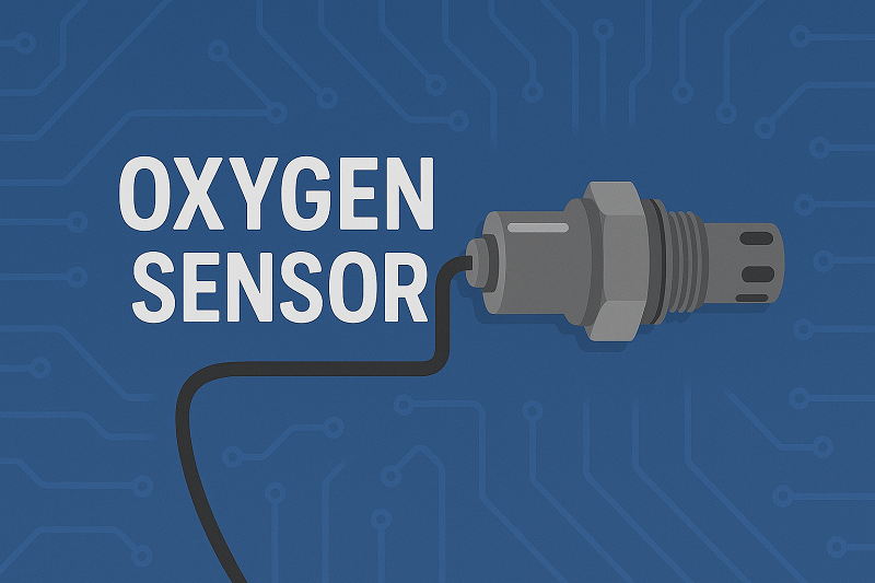 What is an Oxygen Sensor?
24 April 202512935
 Semiconductor Market Poised for Strong Rebound in 2024, Predicts WSTS
11 December 20235100
Intersil (Renesas Electronics America)
In Stock: 1590
United States
China
Canada
Japan
Russia
Germany
United Kingdom
Singapore
Italy
Hong Kong(China)
Taiwan(China)
France
Korea
Mexico
Netherlands
Malaysia
Austria
Spain
Switzerland
Poland
Thailand
Vietnam
India
United Arab Emirates
Afghanistan
Åland Islands
Albania
Algeria
American Samoa
Andorra
Angola
Anguilla
Antigua & Barbuda
Argentina
Armenia
Aruba
Australia
Azerbaijan
Bahamas
Bahrain
Bangladesh
Barbados
Belarus
Belgium
Belize
Benin
Bermuda
Bhutan
Bolivia
Bonaire, Sint Eustatius and Saba
Bosnia & Herzegovina
Botswana
Brazil
British Indian Ocean Territory
British Virgin Islands
Brunei
Bulgaria
Burkina Faso
Burundi
Cabo Verde
Cambodia
Cameroon
Cayman Islands
Central African Republic
Chad
Chile
Christmas Island
Cocos (Keeling) Islands
Colombia
Comoros
Congo
Congo (DRC)
Cook Islands
Costa Rica
Côte d’Ivoire
Croatia
Cuba
Curaçao
Cyprus
Czechia
Denmark
Djibouti
Dominica
Dominican Republic
Ecuador
Egypt
El Salvador
Equatorial Guinea
Eritrea
Estonia
Eswatini
Ethiopia
Falkland Islands
Faroe Islands
Fiji
Finland
French Guiana
French Polynesia
Gabon
Gambia
Georgia
Ghana
Gibraltar
Greece
Greenland
Grenada
Guadeloupe
Guam
Guatemala
Guernsey
Guinea
Guinea-Bissau
Guyana
Haiti
Honduras
Hungary
Iceland
Indonesia
Iran
Iraq
Ireland
Isle of Man
Israel
Jamaica
Jersey
Jordan
Kazakhstan
Kenya
Kiribati
Kosovo
Kuwait
Kyrgyzstan
Laos
Latvia
Lebanon
Lesotho
Liberia
Libya
Liechtenstein
Lithuania
Luxembourg
Macao(China)
Madagascar
Malawi
Maldives
Mali
Malta
Marshall Islands
Martinique
Mauritania
Mauritius
Mayotte
Micronesia
Moldova
Monaco
Mongolia
Montenegro
Montserrat
Morocco
Mozambique
Myanmar
Namibia
Nauru
Nepal
New Caledonia
New Zealand
Nicaragua
Niger
Nigeria
Niue
Norfolk Island
North Korea
North Macedonia
Northern Mariana Islands
Norway
Oman
Pakistan
Palau
Palestinian Authority
Panama
Papua New Guinea
Paraguay
Peru
Philippines
Pitcairn Islands
Portugal
Puerto Rico
Qatar
Réunion
Romania
Rwanda
Samoa
San Marino
São Tomé & Príncipe
Saudi Arabia
Senegal
Serbia
Seychelles
Sierra Leone
Sint Maarten
Slovakia
Slovenia
Solomon Islands
Somalia
South Africa
South Sudan
Sri Lanka
St Helena, Ascension, Tristan da Cunha
St. Barthélemy
St. Kitts & Nevis
St. Lucia
St. Martin
St. Pierre & Miquelon
St. Vincent & Grenadines
Sudan
Suriname
Svalbard & Jan Mayen
Sweden
Syria
Tajikistan
Tanzania
Timor-Leste
Togo
Tokelau
Tonga
Trinidad & Tobago
Tunisia
Turkey
Turkmenistan
Turks & Caicos Islands
Tuvalu
U.S. Outlying Islands
U.S. Virgin Islands
Uganda
Ukraine
Uruguay
Uzbekistan
Vanuatu
Vatican City
Venezuela
Wallis & Futuna
Yemen
Zambia
Zimbabwe
![ISL55001IBZ-T7]() ISL55001IBZ-T7
ISL55001IBZ-T7Intersil (Renesas Electronics America)
![ISL28210FBZ]() ISL28210FBZ
ISL28210FBZIntersil (Renesas Electronics America)
![EL5175IS]() EL5175IS
EL5175ISIntersil (Renesas Electronics America)
![ISL28213FUZ-T7]() ISL28213FUZ-T7
ISL28213FUZ-T7Intersil (Renesas Electronics America)
![CA3140E]() CA3140E
CA3140EIntersil (Renesas Electronics America)
![ISL28158FBZ]() ISL28158FBZ
ISL28158FBZIntersil (Renesas Electronics America)
![CA3140EZ]() CA3140EZ
CA3140EZIntersil (Renesas Electronics America)
![ISL55002IBZ-T7]() ISL55002IBZ-T7
ISL55002IBZ-T7Intersil (Renesas Electronics America)
![CA3140AEZ]() CA3140AEZ
CA3140AEZIntersil (Renesas Electronics America)


