
 Product
 Brand
Brand Articles
 Tools
Tools
Comprehensive Introduction to LM393D Comparator [Video]

Surface Mount Tube 18mA mA 1.3 μs μs Linear Comparators 106.02dB dB 250nA pA 1mA μA 1mV mV Surface Mount


Surface Mount Tube 18mA mA 1.3 μs μs Linear Comparators 106.02dB dB 250nA pA 1mA μA 1mV mV Surface Mount
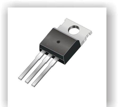
LM393D is a low-power, dual-voltage comparator. This blog mainly introduces pinout, specifications, applications, and other detailed information about STMicroelectronics LM393D.

LM393 Comparator for Noobs (with test circuit)
LM393D Description
The LM393 devices consist of two independent low voltage comparators designed specifically to operate from a single supply over a wide range of voltages. Operation from split power supplies is also possible. These comparators also have a unique characteristic in that the input common-mode voltage range includes ground even though operated from a single power supply voltage.
LM393D Pin Connections

LM393D CAD model
LM393D Features
Wide single-supply voltage range or dual supplies: 2 V to 36 V or ±1 V to ±18 V
Very low supply current (0.45 mA) independent of supply voltage (1 mW/comparator at 5 V)
Low input bias current: 20 nA typ.
Low input offset current: ±3 nA typ.
Low input offset voltage: ±1 mV typ.
Input common-mode voltage range includesground
Low output saturation voltage: 80 mV typ. (Isink = 4 mA)
Differential input voltage range equal to the supply voltage
TTL, DTL, ECL, MOS, CMOS compatible outputs
Specifications
- TypeParameter
- Lifecycle Status
Lifecycle Status refers to the current stage of an electronic component in its product life cycle, indicating whether it is active, obsolete, or transitioning between these states. An active status means the component is in production and available for purchase. An obsolete status indicates that the component is no longer being manufactured or supported, and manufacturers typically provide a limited time frame for support. Understanding the lifecycle status is crucial for design engineers to ensure continuity and reliability in their projects.
ACTIVE (Last Updated: 7 months ago) - Factory Lead Time25 Weeks
- Mount
In electronic components, the term "Mount" typically refers to the method or process of physically attaching or fixing a component onto a circuit board or other electronic device. This can involve soldering, adhesive bonding, or other techniques to secure the component in place. The mounting process is crucial for ensuring proper electrical connections and mechanical stability within the electronic system. Different components may have specific mounting requirements based on their size, shape, and function, and manufacturers provide guidelines for proper mounting procedures to ensure optimal performance and reliability of the electronic device.
Surface Mount - Mounting Type
The "Mounting Type" in electronic components refers to the method used to attach or connect a component to a circuit board or other substrate, such as through-hole, surface-mount, or panel mount.
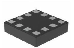
Surface Mount - Package / Case
refers to the protective housing that encases an electronic component, providing mechanical support, electrical connections, and thermal management.
8-SOIC (0.154, 3.90mm Width) - Number of Pins8
- Weight4.535924g
- Operating Temperature
The operating temperature is the range of ambient temperature within which a power supply, or any other electrical equipment, operate in. This ranges from a minimum operating temperature, to a peak or maximum operating temperature, outside which, the power supply may fail.
0°C~70°C - Packaging
Semiconductor package is a carrier / shell used to contain and cover one or more semiconductor components or integrated circuits. The material of the shell can be metal, plastic, glass or ceramic.
Tube - JESD-609 Code
The "JESD-609 Code" in electronic components refers to a standardized marking code that indicates the lead-free solder composition and finish of electronic components for compliance with environmental regulations.
e4 - Part Status
Parts can have many statuses as they progress through the configuration, analysis, review, and approval stages.
Active - Moisture Sensitivity Level (MSL)
Moisture Sensitivity Level (MSL) is a standardized rating that indicates the susceptibility of electronic components, particularly semiconductors, to moisture-induced damage during storage and the soldering process, defining the allowable exposure time to ambient conditions before they require special handling or baking to prevent failures
1 (Unlimited) - Number of Terminations8
- ECCN Code
An ECCN (Export Control Classification Number) is an alphanumeric code used by the U.S. Bureau of Industry and Security to identify and categorize electronic components and other dual-use items that may require an export license based on their technical characteristics and potential for military use.
EAR99 - TypeGeneral Purpose
- Terminal Finish
Terminal Finish refers to the surface treatment applied to the terminals or leads of electronic components to enhance their performance and longevity. It can improve solderability, corrosion resistance, and overall reliability of the connection in electronic assemblies. Common finishes include nickel, gold, and tin, each possessing distinct properties suitable for various applications. The choice of terminal finish can significantly impact the durability and effectiveness of electronic devices.
Nickel/Palladium/Gold (Ni/Pd/Au) - Max Power Dissipation
The maximum power that the MOSFET can dissipate continuously under the specified thermal conditions.
710mW - Terminal Position
In electronic components, the term "Terminal Position" refers to the physical location of the connection points on the component where external electrical connections can be made. These connection points, known as terminals, are typically used to attach wires, leads, or other components to the main body of the electronic component. The terminal position is important for ensuring proper connectivity and functionality of the component within a circuit. It is often specified in technical datasheets or component specifications to help designers and engineers understand how to properly integrate the component into their circuit designs.
DUAL - Terminal Form
Occurring at or forming the end of a series, succession, or the like; closing; concluding.
GULL WING - Peak Reflow Temperature (Cel)
Peak Reflow Temperature (Cel) is a parameter that specifies the maximum temperature at which an electronic component can be exposed during the reflow soldering process. Reflow soldering is a common method used to attach electronic components to a circuit board. The Peak Reflow Temperature is crucial because it ensures that the component is not damaged or degraded during the soldering process. Exceeding the specified Peak Reflow Temperature can lead to issues such as component failure, reduced performance, or even permanent damage to the component. It is important for manufacturers and assemblers to adhere to the recommended Peak Reflow Temperature to ensure the reliability and functionality of the electronic components.
260 - Number of Functions2
- Supply Voltage
Supply voltage refers to the electrical potential difference provided to an electronic component or circuit. It is crucial for the proper operation of devices, as it powers their functions and determines performance characteristics. The supply voltage must be within specified limits to ensure reliability and prevent damage to components. Different electronic devices have specific supply voltage requirements, which can vary widely depending on their design and intended application.
5V - Time@Peak Reflow Temperature-Max (s)
Time@Peak Reflow Temperature-Max (s) refers to the maximum duration that an electronic component can be exposed to the peak reflow temperature during the soldering process, which is crucial for ensuring reliable solder joint formation without damaging the component.
30 - Base Part Number
The "Base Part Number" (BPN) in electronic components serves a similar purpose to the "Base Product Number." It refers to the primary identifier for a component that captures the essential characteristics shared by a group of similar components. The BPN provides a fundamental way to reference a family or series of components without specifying all the variations and specific details.
LM393 - Pin Count
a count of all of the component leads (or pins)
8 - Output Type
The "Output Type" parameter in electronic components refers to the type of signal or data that is produced by the component as an output. This parameter specifies the nature of the output signal, such as analog or digital, and can also include details about the voltage levels, current levels, frequency, and other characteristics of the output signal. Understanding the output type of a component is crucial for ensuring compatibility with other components in a circuit or system, as well as for determining how the output signal can be utilized or processed further. In summary, the output type parameter provides essential information about the nature of the signal that is generated by the electronic component as its output.
CMOS, DTL, ECL, MOS, Open-Collector, TTL - Power Supplies
an electronic circuit that converts the voltage of an alternating current (AC) into a direct current (DC) voltage.?
5V - Number of Circuits2
- Nominal Supply Current
Nominal current is the same as the rated current. It is the current drawn by the motor while delivering rated mechanical output at its shaft.
1mA - Power Dissipation
the process by which an electronic or electrical device produces heat (energy loss or waste) as an undesirable derivative of its primary action.
710mW - Output Current
The rated output current is the maximum load current that a power supply can provide at a specified ambient temperature. A power supply can never provide more current that it's rated output current unless there is a fault, such as short circuit at the load.
18mA - Max Supply Current
Max Supply Current refers to the maximum amount of electrical current that a component can draw from its power supply under normal operating conditions. It is a critical parameter that ensures the component operates reliably without exceeding its thermal limits or damaging internal circuitry. Exceeding this current can lead to overheating, performance degradation, or failure of the component. Understanding this parameter is essential for designing circuits that provide adequate power while avoiding overload situations.
1mA - Propagation Delay
the flight time of packets over the transmission link and is limited by the speed of light.
1.3 μs - Quiescent Current
The quiescent current is defined as the current level in the amplifier when it is producing an output of zero.
2.5mA - Turn On Delay Time
Turn-on delay, td(on), is the time taken to charge the input capacitance of the device before drain current conduction can start.
1.3 μs - Response Time
the time taken for a circuit or measuring device, when subjected to a change in input signal, to change its state by a specified fraction of its total response to that change.
1.3 μs - Voltage - Supply, Single/Dual (±)
The parameter "Voltage - Supply, Single/Dual (±)" in electronic components refers to the power supply voltage required for the proper operation of the component. This parameter indicates whether the component requires a single power supply voltage (e.g., 5V) or a dual power supply voltage (e.g., ±15V). For components that require a single power supply voltage, only one voltage level is needed for operation. On the other hand, components that require a dual power supply voltage need both positive and negative voltage levels to function correctly.Understanding the voltage supply requirements of electronic components is crucial for designing and integrating them into circuits to ensure proper functionality and prevent damage due to incorrect voltage levels.
2V~36V ±1V~18V - Output Current per Channel
Output Current per Channel is a specification commonly found in electronic components such as amplifiers, audio interfaces, and power supplies. It refers to the maximum amount of electrical current that can be delivered by each individual output channel of the component. This parameter is important because it determines the capacity of the component to drive connected devices or loads. A higher output current per channel means the component can deliver more power to connected devices, while a lower output current may limit the performance or functionality of the component in certain applications. It is crucial to consider the output current per channel when selecting electronic components to ensure they can meet the power requirements of the intended system or setup.
18mA - Input Offset Voltage (Vos)
Input Offset Voltage (Vos) is a key parameter in electronic components, particularly in operational amplifiers. It refers to the voltage difference that must be applied between the two input terminals of the amplifier to nullify the output voltage when the input terminals are shorted together. In simpler terms, it represents the voltage required to bring the output of the amplifier to zero when there is no input signal present. Vos is an important parameter as it can introduce errors in the output signal of the amplifier, especially in precision applications where accuracy is crucial. Minimizing Vos is essential to ensure the amplifier operates with high precision and accuracy.
1mV - Voltage Gain
Voltage gain is a measure of how much an electronic component or circuit amplifies an input voltage signal to produce an output voltage signal. It is typically expressed as a ratio or in decibels (dB). A higher voltage gain indicates a greater amplification of the input signal. Voltage gain is an important parameter in amplifiers, where it determines the level of amplification provided by the circuit. It is calculated by dividing the output voltage by the input voltage and is a key factor in determining the overall performance and functionality of electronic devices.
106.02dB - Average Bias Current-Max (IIB)
The parameter "Average Bias Current-Max (IIB)" in electronic components refers to the maximum average bias current that the component can handle without exceeding its specified operating limits. Bias current is the current that flows through a component when it is in its quiescent state or when it is not actively processing a signal. Exceeding the maximum average bias current can lead to overheating, reduced performance, or even damage to the component. Therefore, it is important to ensure that the bias current does not exceed the specified maximum value to maintain the reliability and longevity of the electronic component.
0.4μA - Supply Voltage Limit-Max
The parameter "Supply Voltage Limit-Max" in electronic components refers to the maximum voltage that the component can safely handle without getting damaged. This specification is crucial for ensuring the reliable operation and longevity of the component within a given electrical system. Exceeding the maximum supply voltage limit can lead to overheating, electrical breakdown, or permanent damage to the component. It is important to carefully adhere to this limit when designing and operating electronic circuits to prevent potential failures and ensure the overall system's performance and safety.
36V - Max Input Current
Max Input Current is a parameter that specifies the maximum amount of electrical current that can safely flow into an electronic component without causing damage. It is an important consideration when designing or using electronic circuits to ensure that the component operates within its specified limits. Exceeding the maximum input current can lead to overheating, component failure, or even pose safety risks. Manufacturers provide this parameter in datasheets to help engineers and users understand the limitations of the component and ensure proper operation within the specified parameters.
250nA - Dual Supply Voltage
Dual Supply Voltage refers to an electronic component's requirement for two separate power supply voltages, typically one positive and one negative. This configuration is commonly used in operational amplifiers, analog circuits, and certain digital devices to allow for greater signal handling capabilities and improved performance. The use of dual supply voltages enables the device to process bipolar signals, thereby enhancing its functionality in various applications.
9V - Input Bias Current
Input Bias Current refers to the small amount of current that flows into the input terminals of an electronic component, such as an operational amplifier. It is primarily caused by the input impedance of the device and the characteristics of the transistors within it. This current is crucial in determining the accuracy of the analog signal processing, as it can affect the level of voltage offset and signal integrity in the application. In many precise applications, minimizing input bias current is essential to achieve optimal performance.
250nA - Max Junction Temperature (Tj)
Max Junction Temperature (Tj) refers to the maximum allowable temperature at the junction of a semiconductor device, such as a transistor or integrated circuit. It is a critical parameter that influences the performance, reliability, and lifespan of the component. Exceeding this temperature can lead to thermal runaway, breakdown, or permanent damage to the device. Proper thermal management is essential to ensure the junction temperature remains within safe operating limits during device operation.
150°C - Voltage - Input Offset (Max)
Voltage - Input Offset (Max) is a parameter that refers to the maximum allowable difference in input voltage between two input terminals of an electronic component, such as an operational amplifier, before the output voltage deviates from the expected value. This parameter is crucial in precision applications where accurate voltage amplification or signal processing is required. A higher value for the input offset voltage indicates a greater potential for error in the output signal, so minimizing this parameter is important for maintaining the accuracy and reliability of the component's performance. Designers often take this parameter into consideration when selecting components for circuits that require precise voltage control and signal processing.
5mV @ 30V - Current - Input Bias (Max)
The parameter "Current - Input Bias (Max)" in electronic components refers to the maximum amount of input bias current that can flow into the input terminal of the component without causing any adverse effects on its performance. Input bias current is the small amount of current that flows into the input terminal of an electronic component, such as an operational amplifier, transistor, or integrated circuit, even when no input signal is applied. This parameter is important because excessive input bias current can lead to errors in the output signal and affect the overall performance of the component. Manufacturers specify a maximum value for input bias current to ensure proper operation and reliability of the component in various applications. It is crucial for designers and engineers to consider this parameter when selecting components for their circuits to ensure optimal performance and functionality.
0.25μA @ 5V - Ambient Temperature Range High
This varies from person to person, but it is somewhere between 68 and 77 degrees F on average. The temperature setting that is comfortable for an individual may fluctuate with humidity and outside temperature as well. The temperature of an air conditioned room can also be considered ambient temperature.
70°C - Natural Thermal Resistance
Natural thermal resistance in electronic components refers to the ability of a device to dissipate heat without the assistance of external cooling methods such as fans or liquid cooling. It is a measure of how effectively a component can transfer heat from its junction to its surrounding environment through natural convection and radiation. This parameter is critical for assessing the thermal performance and reliability of electronic devices, as excessive heat can lead to failure or diminished efficiency. Natural thermal resistance is typically expressed in degrees Celsius per watt (°C/W) and is influenced by factors such as the material properties, component design, and ambient conditions.
125 °C/W - Current - Output (Typ)
The parameter "Current - Output (Typ)" in electronic components refers to the typical output current that the component is designed to deliver under normal operating conditions. It represents the expected or average value of the output current that the component can provide. This parameter is important for determining the capability of the component to supply power to other parts of the circuit or system. It helps in ensuring that the component can meet the current requirements of the application without exceeding its specified limits. Manufacturers provide this parameter in datasheets to help designers select the appropriate component for their specific needs.
18mA @ 5V - Height1.75mm
- Length4.9mm
- Width3.9mm
- REACH SVHC
The parameter "REACH SVHC" in electronic components refers to the compliance with the Registration, Evaluation, Authorization, and Restriction of Chemicals (REACH) regulation regarding Substances of Very High Concern (SVHC). SVHCs are substances that may have serious effects on human health or the environment, and their use is regulated under REACH to ensure their safe handling and minimize their impact.Manufacturers of electronic components need to declare if their products contain any SVHCs above a certain threshold concentration and provide information on the safe use of these substances. This information allows customers to make informed decisions about the potential risks associated with using the components and take appropriate measures to mitigate any hazards.Ensuring compliance with REACH SVHC requirements is essential for electronics manufacturers to meet regulatory standards, protect human health and the environment, and maintain transparency in their supply chain. It also demonstrates a commitment to sustainability and responsible manufacturing practices in the electronics industry.
No SVHC - Radiation Hardening
Radiation hardening is the process of making electronic components and circuits resistant to damage or malfunction caused by high levels of ionizing radiation, especially for environments in outer space (especially beyond the low Earth orbit), around nuclear reactors and particle accelerators, or during nuclear accidents or nuclear warfare.
No - RoHS Status
RoHS means “Restriction of Certain Hazardous Substances” in the “Hazardous Substances Directive” in electrical and electronic equipment.
ROHS3 Compliant - Lead Free
Lead Free is a term used to describe electronic components that do not contain lead as part of their composition. Lead is a toxic material that can have harmful effects on human health and the environment, so the electronics industry has been moving towards lead-free components to reduce these risks. Lead-free components are typically made using alternative materials such as silver, copper, and tin. Manufacturers must comply with regulations such as the Restriction of Hazardous Substances (RoHS) directive to ensure that their products are lead-free and environmentally friendly.
Lead Free
LM393D Block Diagram

LM393D Schematic diagram
LM393D Alternatives
Part Number | Description | Manufacturer |
LM393DG4 AMPLIFIER CIRCUITS | Dual differential comparator, commercial-grade 8-SOIC 0 to 70 | Texas Instruments |
LM393N/NOPE AMPLIFIER CIRCUITS | Low Power Low Offset Voltage Dual Comparator 8-PDIP 0 to 70 | Texas Instruments |
LM393M/NOPE AMPLIFIER CIRCUITS | IC DUAL COMPARATOR, 9000 UV OFFSET-MAX, 1300 ns RESPONSE TIME, PDSO8, LEAD-FREE, SOIC-8, Comparator | National Semiconductor Corporation |
LM393MX/NOPE AMPLIFIER CIRCUITS | Low Power Low Offset Voltage Dual Comparator 8-SOIC 0 to 70 | Texas Instruments |
LM393YDT AMPLIFIER CIRCUITS | DUAL COMPARATOR, 9000uV OFFSET-MAX, 1300ns RESPONSE TIME, PDSO8, LEAD-FREE, MICRO, PLASTIC, SOP-8 | STMicroelectronics |
LM393D AMPLIFIER CIRCUITS | Dual differential comparator, commercial-grade 8-SOIC 0 to 70 | Texas Instruments |
LM393M AMPLIFIER CIRCUITS | Comparator | Bay Linear Inc |
LM393MX_NL AMPLIFIER CIRCUITS | Comparator, 2 Func, 9000uV Offset-Max, 1400ns Response Time, BIPolar, PDSO8, SOP-8 | Fairchild Semiconductor Corporation |
LM393DRG3 AMPLIFIER CIRCUITS | Dual differential comparator, commercial-grade 8-SOIC 0 to 70 | Texas Instruments |
LM393DG AMPLIFIER CIRCUITS | Comparator, Dual, Low Offset Voltage, SOIC-8 Narrow Body, 98-TUBE | ON Semiconductor |
How to use LM393D?
The LM393 applications are very similar to the LM311 Comparator IC, with a few minor differences in requirements. Aside from that, the LM311 can be considered a near substitute for the LM393. The LM393 has both an inverting and non-inverting pin, as do all voltage comparators. The output (pin 7) will be high if the voltage at the Non-Inverting Terminal (pin 2) is higher than the voltage at the Inverting Terminal (pin 2), otherwise, the output will be low.
Since this is the most common configuration for digital circuits, we'll assume the LM393 is operated by a +5V supply voltage circuit. The VCC+ (pin 8) is connected to the +5V supply voltage in this form, while the VCC (pin 4) is grounded to maintain a 0V potential. The Inverting Terminal is set to 2.5V in the circuit below, and the Non-Inverting Terminal voltage is varied with a potentiometer. When pin 2 has a higher voltage than pin 7, the output voltage remains high, and vice versa
If you want to manually change the DC-Offset voltage, use pins 5 and 6 on the Op-amp to set the balance voltage. Normally, these pins are not used because the Input Offset can be managed much better. Pins 5 and 6 should be shorted when not in use, as seen above. You'll also note that the transistor's collector pin (pin 7) is used for output while the emitter pin (pin 1) is grounded; this is known as a "Collector output Circuit," although this isn't always the case.
LM393D Applications
LM393D Manufacturer
STMicroelectronics is a global independent semiconductor company and is a leader in developing and delivering semiconductor solutions across the spectrum of microelectronics applications. An unrivaled combination of silicon and system expertise, manufacturing strength, Intellectual Property (IP) portfolio, and strategic partners positions the Company at the forefront of System-on-Chip (SoC) technology, and its products play a key role in enabling today's convergence trends.
Datasheet PDF
- Datasheets :
Trend Analysis
1.What is the role of LM393?
LM393 is a dual voltage comparator, it has two input terminals and two output terminals, a reference voltage terminal. When the input terminal voltage is lower than the reference voltage, the output terminal is high level, otherwise the output terminal level is reversed.
2.Can LM393 and LM358 be interchangeable?
Generally speaking, they cannot be directly interchanged. Although the op amp can be used as a voltage comparator in some circuits that require less precision, the op amp cannot be replaced by a comparator because there is no amplification function. When 358 is replaced with 393, the original 393 output terminal should be removed. Although the symbols of the pull-resistance comparator and the op amp are the same on the circuit diagram, the two devices do have very big differences and generally cannot be interchanged.
3.What is the difference between "lm293" and "LM393"?
There is little difference between LM293 and LM393. The operating temperature range of LM293 is wider: -25℃~85℃. The operating temperature range of LM393 is narrower: 0℃~70℃. Other indicators are the same or have slight differences. In short, LM293 is better than LM393.
4.How to use lm393 to realize the voltage comparison function?
1: You need a voltage reference. 2: You need two adjustable attenuation circuits (resistance plus potentiometer), one attenuates 22V and one attenuates 25V 3: You need two comparators, an inverting comparison (the reference voltage is connected to the non-inverting terminal. The comparison voltage is connected to the inverting terminal), and a non-inverting comparator. Comparator output can be connected to LED 4: You need an inverter. Connect the output terminals of the two comparators to the inverter. When the two comparators are both high, the inverter outputs a low level. The LED does not light up. And when both comparators are low. The LED is on to indicate that it is in the normal range.
 TMC2130 Driver IC: Datasheet, Pinout and Application
01 September 20213324
 MCP25625 CAN Controller: Datasheet, Block Diagram, Feature
06 October 20213587
 BF888H6327XTSA1 NPN RF Transistor:Datasheet, Pinout and Features
10 August 2021409
 Yageo RC0603FR-0710KL Price Trends Across Suppliers 2025
20 August 20251586
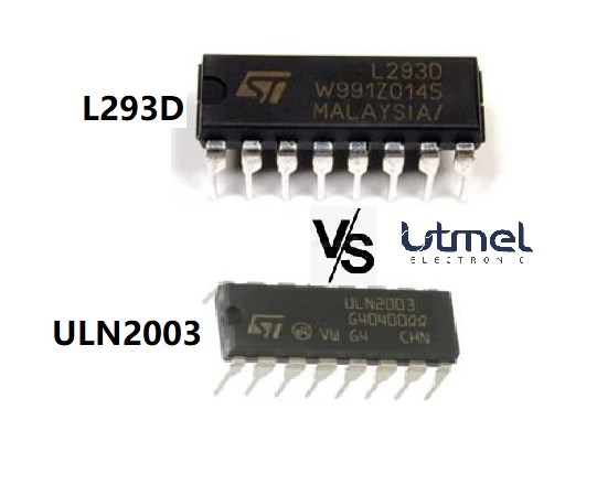 A Comparison Article about L293D & ULN2003
25 April 20227619
 LM4040 Bandgap Reference: Pinout, Equivalent and Datasheet
28 October 20212431
 LIS2DW12TR Motion Sensor: Datasheet, Pinout, Application Hint
07 April 20224906
 2SC2625 NPN Power Transistor: Equivalent, Datasheet pdf and Pinout
12 November 20219399
![PMIC: Basic Types and Applications [Video]](https://res.utmel.com/Images/Article/596928b4-5505-4751-b95b-54949cc0bf7b.jpg) PMIC: Basic Types and Applications [Video]
PMIC: Basic Types and Applications [Video]27 October 20205506
 What are TPMS Sensors?
21 November 20205158
 What causes the Noise of Electronic Equipment when it is Running?
01 August 20222859
 Semiconductor Material Industry Guide
21 January 20227129
 What is Amplifier?
08 November 20257968
 What is a Piezoelectric Sensor?
26 August 202017533
 What is an LDO (Low Dropout Regulator)?
29 October 20216421
 Introduction to Silicon Controlled Rectifier
25 September 20209286
STMicroelectronics
In Stock: 140
United States
China
Canada
Japan
Russia
Germany
United Kingdom
Singapore
Italy
Hong Kong(China)
Taiwan(China)
France
Korea
Mexico
Netherlands
Malaysia
Austria
Spain
Switzerland
Poland
Thailand
Vietnam
India
United Arab Emirates
Afghanistan
Åland Islands
Albania
Algeria
American Samoa
Andorra
Angola
Anguilla
Antigua & Barbuda
Argentina
Armenia
Aruba
Australia
Azerbaijan
Bahamas
Bahrain
Bangladesh
Barbados
Belarus
Belgium
Belize
Benin
Bermuda
Bhutan
Bolivia
Bonaire, Sint Eustatius and Saba
Bosnia & Herzegovina
Botswana
Brazil
British Indian Ocean Territory
British Virgin Islands
Brunei
Bulgaria
Burkina Faso
Burundi
Cabo Verde
Cambodia
Cameroon
Cayman Islands
Central African Republic
Chad
Chile
Christmas Island
Cocos (Keeling) Islands
Colombia
Comoros
Congo
Congo (DRC)
Cook Islands
Costa Rica
Côte d’Ivoire
Croatia
Cuba
Curaçao
Cyprus
Czechia
Denmark
Djibouti
Dominica
Dominican Republic
Ecuador
Egypt
El Salvador
Equatorial Guinea
Eritrea
Estonia
Eswatini
Ethiopia
Falkland Islands
Faroe Islands
Fiji
Finland
French Guiana
French Polynesia
Gabon
Gambia
Georgia
Ghana
Gibraltar
Greece
Greenland
Grenada
Guadeloupe
Guam
Guatemala
Guernsey
Guinea
Guinea-Bissau
Guyana
Haiti
Honduras
Hungary
Iceland
Indonesia
Iran
Iraq
Ireland
Isle of Man
Israel
Jamaica
Jersey
Jordan
Kazakhstan
Kenya
Kiribati
Kosovo
Kuwait
Kyrgyzstan
Laos
Latvia
Lebanon
Lesotho
Liberia
Libya
Liechtenstein
Lithuania
Luxembourg
Macao(China)
Madagascar
Malawi
Maldives
Mali
Malta
Marshall Islands
Martinique
Mauritania
Mauritius
Mayotte
Micronesia
Moldova
Monaco
Mongolia
Montenegro
Montserrat
Morocco
Mozambique
Myanmar
Namibia
Nauru
Nepal
New Caledonia
New Zealand
Nicaragua
Niger
Nigeria
Niue
Norfolk Island
North Korea
North Macedonia
Northern Mariana Islands
Norway
Oman
Pakistan
Palau
Palestinian Authority
Panama
Papua New Guinea
Paraguay
Peru
Philippines
Pitcairn Islands
Portugal
Puerto Rico
Qatar
Réunion
Romania
Rwanda
Samoa
San Marino
São Tomé & Príncipe
Saudi Arabia
Senegal
Serbia
Seychelles
Sierra Leone
Sint Maarten
Slovakia
Slovenia
Solomon Islands
Somalia
South Africa
South Sudan
Sri Lanka
St Helena, Ascension, Tristan da Cunha
St. Barthélemy
St. Kitts & Nevis
St. Lucia
St. Martin
St. Pierre & Miquelon
St. Vincent & Grenadines
Sudan
Suriname
Svalbard & Jan Mayen
Sweden
Syria
Tajikistan
Tanzania
Timor-Leste
Togo
Tokelau
Tonga
Trinidad & Tobago
Tunisia
Turkey
Turkmenistan
Turks & Caicos Islands
Tuvalu
U.S. Outlying Islands
U.S. Virgin Islands
Uganda
Ukraine
Uruguay
Uzbekistan
Vanuatu
Vatican City
Venezuela
Wallis & Futuna
Yemen
Zambia
Zimbabwe


