
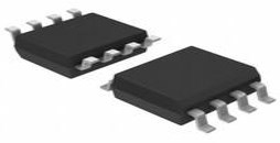
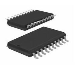
LM211QD Voltage Comparator Overview

Surface Mount Tube 50mA mA 165 ns μs Linear Comparators 106.02dB dB 100nA pA 6mA μA 3mV mV Surface Mount
Unit Price: $0.501516
Ext Price: $0.50


Surface Mount Tube 50mA mA 165 ns μs Linear Comparators 106.02dB dB 100nA pA 6mA μA 3mV mV Surface Mount
The LM211QD device is a single high-speed voltage comparator. The LM211 devices are designed to operate from a wide range of powersupply voltages, including ±15-V supplies for operational amplifiers and 5-V supplies for logic systems.
LM211QD Pinout


Pin Functions
LM211QD CAD Model
LM211QD symbol

LM211QD footprint

LM211QD 3D Model

LM211QD Features
• Fast Response Time: 165 ns
• Strobe Capability
• Maximum Input Bias Current: 300 nA
• Maximum Input Offset Current: 70 nA
• Can Operate From Single 5-V Supply
• Available in Q-Temp Automotive
– High-Reliability Automotive Applications
– Configuration Control and Print Support
– Qualification to Automotive Standards
• On Products Compliant to MIL-PRF-38535, All Parameters Are Tested Unless Otherwise Noted. On All Other Products, Production Processing Does Not Necessarily Include Testing of All Parameters.
LMx11 Feature Description
LMx11 consists of a PNP input stage to sense voltages near VCC–. It also contains balance and strobe pins forexternal offset adjustment or trimming.
The input stage is followed by a very high gain stage for the very fast response after a voltage difference on the input pins has been sensed.
This is then followed by the output stage that consists of an open collector NPN (pulldown or low-side) transistor.
Unlike most open-drain comparators, this NPN output stage has an isolated emitter from VCC–, allowing this device to set the VOL output value for collector output.
LM211QD Advantage
The characteristics of this high-gain LM211QD comparator circuit from Texas Instruments allow it to compare input voltages or currents. It has an open collector/emitter output. Its typical dual supply voltage is ±3|±5|±9|±12 V, with a minimum of ±1.75 V and maximum of ±15 V. This comparator has a minimum operating temperature of -40 °C and a maximum of 125 °C. This device uses one or two power supplies. This device is made with bipolar technology. It has a single channel per chip.
The output levels are compatible with most TTL and MOS circuits. The LM111, LM211, and LM311 devices comparators are capable of driving lamps or relays and switching voltages up to 50 V at 50 mA. All inputs and outputs can be isolated from the system ground. The outputs can drive loads referenced to ground, VCC+ or VCC−. Offset balancing and strobe capabilities are available, and the outputs can be wire-OR connected. If the strobe is low, the output is in the off state, regardless of the differential input.
Specifications
- TypeParameter
- Lifecycle Status
Lifecycle Status refers to the current stage of an electronic component in its product life cycle, indicating whether it is active, obsolete, or transitioning between these states. An active status means the component is in production and available for purchase. An obsolete status indicates that the component is no longer being manufactured or supported, and manufacturers typically provide a limited time frame for support. Understanding the lifecycle status is crucial for design engineers to ensure continuity and reliability in their projects.
ACTIVE (Last Updated: 1 day ago) - Factory Lead Time8 Weeks
- Mount
In electronic components, the term "Mount" typically refers to the method or process of physically attaching or fixing a component onto a circuit board or other electronic device. This can involve soldering, adhesive bonding, or other techniques to secure the component in place. The mounting process is crucial for ensuring proper electrical connections and mechanical stability within the electronic system. Different components may have specific mounting requirements based on their size, shape, and function, and manufacturers provide guidelines for proper mounting procedures to ensure optimal performance and reliability of the electronic device.
Surface Mount - Mounting Type
The "Mounting Type" in electronic components refers to the method used to attach or connect a component to a circuit board or other substrate, such as through-hole, surface-mount, or panel mount.
Surface Mount - Package / Case
refers to the protective housing that encases an electronic component, providing mechanical support, electrical connections, and thermal management.
8-SOIC (0.154, 3.90mm Width) - Number of Pins8
- Number of Elements1
- Operating Temperature
The operating temperature is the range of ambient temperature within which a power supply, or any other electrical equipment, operate in. This ranges from a minimum operating temperature, to a peak or maximum operating temperature, outside which, the power supply may fail.
-40°C~125°C - Packaging
Semiconductor package is a carrier / shell used to contain and cover one or more semiconductor components or integrated circuits. The material of the shell can be metal, plastic, glass or ceramic.
Tube - JESD-609 Code
The "JESD-609 Code" in electronic components refers to a standardized marking code that indicates the lead-free solder composition and finish of electronic components for compliance with environmental regulations.
e4 - Pbfree Code
The "Pbfree Code" parameter in electronic components refers to the code or marking used to indicate that the component is lead-free. Lead (Pb) is a toxic substance that has been widely used in electronic components for many years, but due to environmental concerns, there has been a shift towards lead-free alternatives. The Pbfree Code helps manufacturers and users easily identify components that do not contain lead, ensuring compliance with regulations and promoting environmentally friendly practices. It is important to pay attention to the Pbfree Code when selecting electronic components to ensure they meet the necessary requirements for lead-free applications.
yes - Part Status
Parts can have many statuses as they progress through the configuration, analysis, review, and approval stages.
Active - Moisture Sensitivity Level (MSL)
Moisture Sensitivity Level (MSL) is a standardized rating that indicates the susceptibility of electronic components, particularly semiconductors, to moisture-induced damage during storage and the soldering process, defining the allowable exposure time to ambient conditions before they require special handling or baking to prevent failures
1 (Unlimited) - Number of Terminations8
- ECCN Code
An ECCN (Export Control Classification Number) is an alphanumeric code used by the U.S. Bureau of Industry and Security to identify and categorize electronic components and other dual-use items that may require an export license based on their technical characteristics and potential for military use.
EAR99 - TypeGeneral Purpose
- Terminal Finish
Terminal Finish refers to the surface treatment applied to the terminals or leads of electronic components to enhance their performance and longevity. It can improve solderability, corrosion resistance, and overall reliability of the connection in electronic assemblies. Common finishes include nickel, gold, and tin, each possessing distinct properties suitable for various applications. The choice of terminal finish can significantly impact the durability and effectiveness of electronic devices.
Nickel/Palladium/Gold (Ni/Pd/Au) - Terminal Position
In electronic components, the term "Terminal Position" refers to the physical location of the connection points on the component where external electrical connections can be made. These connection points, known as terminals, are typically used to attach wires, leads, or other components to the main body of the electronic component. The terminal position is important for ensuring proper connectivity and functionality of the component within a circuit. It is often specified in technical datasheets or component specifications to help designers and engineers understand how to properly integrate the component into their circuit designs.
DUAL - Terminal Form
Occurring at or forming the end of a series, succession, or the like; closing; concluding.
GULL WING - Peak Reflow Temperature (Cel)
Peak Reflow Temperature (Cel) is a parameter that specifies the maximum temperature at which an electronic component can be exposed during the reflow soldering process. Reflow soldering is a common method used to attach electronic components to a circuit board. The Peak Reflow Temperature is crucial because it ensures that the component is not damaged or degraded during the soldering process. Exceeding the specified Peak Reflow Temperature can lead to issues such as component failure, reduced performance, or even permanent damage to the component. It is important for manufacturers and assemblers to adhere to the recommended Peak Reflow Temperature to ensure the reliability and functionality of the electronic components.
260 - Number of Functions1
- Supply Voltage
Supply voltage refers to the electrical potential difference provided to an electronic component or circuit. It is crucial for the proper operation of devices, as it powers their functions and determines performance characteristics. The supply voltage must be within specified limits to ensure reliability and prevent damage to components. Different electronic devices have specific supply voltage requirements, which can vary widely depending on their design and intended application.
15V - Base Part Number
The "Base Part Number" (BPN) in electronic components serves a similar purpose to the "Base Product Number." It refers to the primary identifier for a component that captures the essential characteristics shared by a group of similar components. The BPN provides a fundamental way to reference a family or series of components without specifying all the variations and specific details.
LM211 - Pin Count
a count of all of the component leads (or pins)
8 - Output Type
The "Output Type" parameter in electronic components refers to the type of signal or data that is produced by the component as an output. This parameter specifies the nature of the output signal, such as analog or digital, and can also include details about the voltage levels, current levels, frequency, and other characteristics of the output signal. Understanding the output type of a component is crucial for ensuring compatibility with other components in a circuit or system, as well as for determining how the output signal can be utilized or processed further. In summary, the output type parameter provides essential information about the nature of the signal that is generated by the electronic component as its output.
DTL, MOS, Open-Collector, Open-Emitter, RTL, TTL - Operating Supply Voltage
The voltage level by which an electrical system is designated and to which certain operating characteristics of the system are related.
28V - Nominal Supply Current
Nominal current is the same as the rated current. It is the current drawn by the motor while delivering rated mechanical output at its shaft.
6mA - Output Current
The rated output current is the maximum load current that a power supply can provide at a specified ambient temperature. A power supply can never provide more current that it's rated output current unless there is a fault, such as short circuit at the load.
50mA - Max Supply Current
Max Supply Current refers to the maximum amount of electrical current that a component can draw from its power supply under normal operating conditions. It is a critical parameter that ensures the component operates reliably without exceeding its thermal limits or damaging internal circuitry. Exceeding this current can lead to overheating, performance degradation, or failure of the component. Understanding this parameter is essential for designing circuits that provide adequate power while avoiding overload situations.
6mA - Quiescent Current
The quiescent current is defined as the current level in the amplifier when it is producing an output of zero.
6mA - Response Time
the time taken for a circuit or measuring device, when subjected to a change in input signal, to change its state by a specified fraction of its total response to that change.
165 ns - Voltage - Supply, Single/Dual (±)
The parameter "Voltage - Supply, Single/Dual (±)" in electronic components refers to the power supply voltage required for the proper operation of the component. This parameter indicates whether the component requires a single power supply voltage (e.g., 5V) or a dual power supply voltage (e.g., ±15V). For components that require a single power supply voltage, only one voltage level is needed for operation. On the other hand, components that require a dual power supply voltage need both positive and negative voltage levels to function correctly.Understanding the voltage supply requirements of electronic components is crucial for designing and integrating them into circuits to ensure proper functionality and prevent damage due to incorrect voltage levels.
3.5V~30V ±1.75V~15V - Output Current per Channel
Output Current per Channel is a specification commonly found in electronic components such as amplifiers, audio interfaces, and power supplies. It refers to the maximum amount of electrical current that can be delivered by each individual output channel of the component. This parameter is important because it determines the capacity of the component to drive connected devices or loads. A higher output current per channel means the component can deliver more power to connected devices, while a lower output current may limit the performance or functionality of the component in certain applications. It is crucial to consider the output current per channel when selecting electronic components to ensure they can meet the power requirements of the intended system or setup.
50mA - Input Offset Voltage (Vos)
Input Offset Voltage (Vos) is a key parameter in electronic components, particularly in operational amplifiers. It refers to the voltage difference that must be applied between the two input terminals of the amplifier to nullify the output voltage when the input terminals are shorted together. In simpler terms, it represents the voltage required to bring the output of the amplifier to zero when there is no input signal present. Vos is an important parameter as it can introduce errors in the output signal of the amplifier, especially in precision applications where accuracy is crucial. Minimizing Vos is essential to ensure the amplifier operates with high precision and accuracy.
3mV - Neg Supply Voltage-Nom (Vsup)
The parameter "Neg Supply Voltage-Nom (Vsup)" in electronic components refers to the nominal negative supply voltage that the component requires to operate within its specified performance characteristics. This parameter indicates the minimum voltage level that must be provided to the component's negative supply pin for proper functionality. It is important to ensure that the negative supply voltage provided to the component does not exceed the maximum specified value to prevent damage or malfunction. Understanding and adhering to the specified negative supply voltage requirements is crucial for the reliable operation of the electronic component in a circuit.
-15V - Voltage Gain
Voltage gain is a measure of how much an electronic component or circuit amplifies an input voltage signal to produce an output voltage signal. It is typically expressed as a ratio or in decibels (dB). A higher voltage gain indicates a greater amplification of the input signal. Voltage gain is an important parameter in amplifiers, where it determines the level of amplification provided by the circuit. It is calculated by dividing the output voltage by the input voltage and is a key factor in determining the overall performance and functionality of electronic devices.
106.02dB - Dual Supply Voltage
Dual Supply Voltage refers to an electronic component's requirement for two separate power supply voltages, typically one positive and one negative. This configuration is commonly used in operational amplifiers, analog circuits, and certain digital devices to allow for greater signal handling capabilities and improved performance. The use of dual supply voltages enables the device to process bipolar signals, thereby enhancing its functionality in various applications.
9V - Input Bias Current
Input Bias Current refers to the small amount of current that flows into the input terminals of an electronic component, such as an operational amplifier. It is primarily caused by the input impedance of the device and the characteristics of the transistors within it. This current is crucial in determining the accuracy of the analog signal processing, as it can affect the level of voltage offset and signal integrity in the application. In many precise applications, minimizing input bias current is essential to achieve optimal performance.
100nA - Voltage - Input Offset (Max)
Voltage - Input Offset (Max) is a parameter that refers to the maximum allowable difference in input voltage between two input terminals of an electronic component, such as an operational amplifier, before the output voltage deviates from the expected value. This parameter is crucial in precision applications where accurate voltage amplification or signal processing is required. A higher value for the input offset voltage indicates a greater potential for error in the output signal, so minimizing this parameter is important for maintaining the accuracy and reliability of the component's performance. Designers often take this parameter into consideration when selecting components for circuits that require precise voltage control and signal processing.
3mV @ ±15V - Current - Input Bias (Max)
The parameter "Current - Input Bias (Max)" in electronic components refers to the maximum amount of input bias current that can flow into the input terminal of the component without causing any adverse effects on its performance. Input bias current is the small amount of current that flows into the input terminal of an electronic component, such as an operational amplifier, transistor, or integrated circuit, even when no input signal is applied. This parameter is important because excessive input bias current can lead to errors in the output signal and affect the overall performance of the component. Manufacturers specify a maximum value for input bias current to ensure proper operation and reliability of the component in various applications. It is crucial for designers and engineers to consider this parameter when selecting components for their circuits to ensure optimal performance and functionality.
0.1μA @ ±15V - Height1.75mm
- Length4.9mm
- Width3.91mm
- Thickness
Thickness in electronic components refers to the measurement of how thick a particular material or layer is within the component structure. It can pertain to various aspects, such as the thickness of a substrate, a dielectric layer, or conductive traces. This parameter is crucial as it impacts the electrical, mechanical, and thermal properties of the component, influencing its performance and reliability in electronic circuits.
1.58mm - REACH SVHC
The parameter "REACH SVHC" in electronic components refers to the compliance with the Registration, Evaluation, Authorization, and Restriction of Chemicals (REACH) regulation regarding Substances of Very High Concern (SVHC). SVHCs are substances that may have serious effects on human health or the environment, and their use is regulated under REACH to ensure their safe handling and minimize their impact.Manufacturers of electronic components need to declare if their products contain any SVHCs above a certain threshold concentration and provide information on the safe use of these substances. This information allows customers to make informed decisions about the potential risks associated with using the components and take appropriate measures to mitigate any hazards.Ensuring compliance with REACH SVHC requirements is essential for electronics manufacturers to meet regulatory standards, protect human health and the environment, and maintain transparency in their supply chain. It also demonstrates a commitment to sustainability and responsible manufacturing practices in the electronics industry.
No SVHC - Radiation Hardening
Radiation hardening is the process of making electronic components and circuits resistant to damage or malfunction caused by high levels of ionizing radiation, especially for environments in outer space (especially beyond the low Earth orbit), around nuclear reactors and particle accelerators, or during nuclear accidents or nuclear warfare.
No - RoHS Status
RoHS means “Restriction of Certain Hazardous Substances” in the “Hazardous Substances Directive” in electrical and electronic equipment.
ROHS3 Compliant - Lead Free
Lead Free is a term used to describe electronic components that do not contain lead as part of their composition. Lead is a toxic material that can have harmful effects on human health and the environment, so the electronics industry has been moving towards lead-free components to reduce these risks. Lead-free components are typically made using alternative materials such as silver, copper, and tin. Manufacturers must comply with regulations such as the Restriction of Hazardous Substances (RoHS) directive to ensure that their products are lead-free and environmentally friendly.
Lead Free
LM211QD Functional Block Diagram

LM211QD Alternative
Part Number | Description | Manufacturer |
LM211QDG4 | Differential Comparator With Strobes 8-SOIC -40 to 125 | Texas Instruments |
LM211QDRQ1 | Automotive Catalog Differential Comparator With Strobes 8-SOIC -40 to 125 | Texas Instruments |
LM211DG4 | Differential Comparator With Strobes 8-SOIC -40 to 85 | Texas Instruments |
LM211DRG4 | Differential Comparator With Strobes 8-SOIC -40 to 85 | Texas Instruments |
LM211DR | Differential Comparator With Strobes 8-SOIC -40 to 85 | Texas Instruments |
LM211QDR | Differential Comparator With Strobes 8-SOIC -40 to 125 | Texas Instruments |
LM211QDRG4Q1 | Automotive Catalog Differential Comparator With Strobes 8-SOIC -40 to 125 | Texas Instruments |
LM211DE4 | Differential Comparator With Strobes 8-SOIC -40 to 85 | Texas Instruments |
LM211D | COMPARATOR, 4000uV OFFSET-MAX, 200ns RESPONSE TIME, PDSO8, PLASTIC, SO-8 | Motorola Mobility LLC |
V62/03638-01XE | Enhanced Product Differential Comparator With Strobes 8-SOIC -40 to 125 | Texas Instruments |
LM211QD Application
• Desktop PCs
• Body Control Modules
• White Goods
• Building Automation
• Oscillators
• Peak Detectors
LM211QD Package & Dimension
Packing information

Tape and reel information

Box dimensions

Parts with Similar Specs
- ImagePart NumberManufacturerPackage / CaseNumber of PinsInput Offset Voltage (Vos)Supply VoltageCurrent - Input Bias (Max)Voltage - Input Offset (Max)Output TypeInput Bias CurrentView Compare
![LM211QD]()
LM211QD
8-SOIC (0.154, 3.90mm Width)
8
3 mV
15 V
0.1μA @ ±15V
3mV @ ±15V
DTL, MOS, Open-Collector, Open-Emitter, RTL, TTL
100 nA
![LM211DR2G]()
8-SOIC (0.154, 3.90mm Width)
8
3 mV
15 V
0.1μA @ ±15V
3mV @ ±15V
DTL, MOS, Open-Collector, Open-Emitter, RTL, TTL
100 nA
![LM211DRG4]()
8-SOIC (0.154, 3.90mm Width)
8
3 mV
15 V
0.1μA @ ±15V
3mV @ ±15V
DTL, MOS, Open-Collector, Open-Emitter, RTL, TTL
100 nA
![LM211D]()
8-SOIC (0.154, 3.90mm Width)
8
3 mV
15 V
0.1μA @ ±15V
3mV @ ±15V
DTL, MOS, Open-Collector, Open-Emitter, RTL, TTL
100 nA
![LM211DR]()
8-SOIC (0.154, 3.90mm Width)
8
700 μV
15 V
0.1μA @ ±15V
3mV @ ±15V
DTL, MOS, Open-Collector, Open-Emitter, RTL, TTL
100 nA


LM211QD Manufacturer
As a global semiconductor company operating in 35 countries, Texas Instruments (TI) is first and foremost a reflection of its people. From the TIer who unveiled the first working integrated circuit in 1958 to the more than 30,000 TIers around the world today who design, manufacture, and sell analog and embedded processing chips, we are problem-solvers collaborating to change the world through technology.
Datasheet PDF
- PCN Design/Specification :
- PCN Assembly/Origin :
Trend Analysis
1.What are LMX11?
The LM111, LM211 and LM311 are voltage comparators that have input currents nearly a thousand times lower than legacy standard devices. They are also designed to operate over a wider range of supply voltages: from standard ±15V op amp supplies down to the single 5-V supply used for IC logic. Their output is compatible with RTL, DTL and TTL as well as MOS circuits. Further, they can drive lamps or relays, switching voltages up to 50V at currents as high as 50 mA.
2.What is the temperature range of LM211Q?
The LM211Q has a temperature range of −40°C to +125°C.
3.What is a comparator used for?
A comparator circuit compares two voltages and outputs either a 1 (the voltage at the plus side; VDD in the illustration) or a 0 (the voltage at the negative side) to indicate which is larger. Comparators are often used, for example, to check whether an input has reached some predetermined value.
4.What are the basic comparators?
A basic op-amp comparator circuit can be used to detect either a positive or a negative going input voltage depending upon which input of the operational amplifier we connect the fixed reference voltage source and the input voltage too.
5.What are the types of comparator?
Comparators are classified into various kinds, such as electronic, electrical, mechanical, optical, sigma, digital and pneumatic comparators, these are used in various applications. Comparators play an essential role in designing electrical and electronic projects.
 MOC3052 Photocoupler: Datasheet, Alternatives and Pinout
16 August 20217133
 KSP2222A NPN Transistor: Pinout, Datasheet and Equivalents
03 November 20217108
 VIPER22A SMPS Controller IC: Circuit, Equivalent and Datasheet
15 September 202134240
 AD7572 Analog to Digital Converter: High-Performance Data Acquisition Solution
06 March 2024179
 MCP73831T Controller: Pinout, Datasheet and Circuit
22 July 2021907
 MV104 Diode: Datasheet, Alternatives and Application Circuit
23 September 20211201
 A Comprehensive Guide to LTC6811HG-2#3ZZTRPBF Battery Management PMIC
06 March 2024223
 ADM3053BRWZ CAN Bus Transceivers: 5.5 V, SOIC and ADM3053 CAN Stock
22 February 20222186
 How to Distinguish MOSFET? Is it N-Channel or P-Channel?
23 December 202110285
 What is Flexible Sensor?
30 May 20225141
 What is a Decoder?
09 January 202617803
 Three Phase Inverter - 180 Degree Conduction Mode
05 October 202316498
 Understanding SiC MOSFET Power Modules and Ensuring its Short-Circuit Safety
15 March 20242349
 How do Inductors Work?
27 October 202514043
 Enhancing the Efficiency of Semiconductors by Using the Spin of Electrons
11 February 20251106
 Does the Terminal Resistance of the CAN Bus Have to be 120Ω?
19 April 202233826
Texas Instruments
In Stock: 30
Minimum: 1 Multiples: 1
Qty
Unit Price
Ext Price
1
$0.501516
$0.50
10
$0.473128
$4.73
100
$0.446347
$44.63
500
$0.421083
$210.54
1000
$0.397248
$397.25
Not the price you want? Send RFQ Now and we'll contact you ASAP.
Inquire for More Quantity
![LMC7225IM5X]() LMC7225IM5X
LMC7225IM5XTexas Instruments
![LM393ADR]() LM393ADR
LM393ADRTexas Instruments
![LM339DR]() LM339DR
LM339DRTexas Instruments
![LM393DR]() LM393DR
LM393DRTexas Instruments
![LM311DR]() LM311DR
LM311DRTexas Instruments
![LM311P]() LM311P
LM311PTexas Instruments
![LM311M/NOPB]() LM311M/NOPB
LM311M/NOPBTexas Instruments
![LM239DR]() LM239DR
LM239DRTexas Instruments
![LM293ADR]() LM293ADR
LM293ADRTexas Instruments
![LM2903DGKR]() LM2903DGKR
LM2903DGKRTexas Instruments


