

 Product
 Brand
Brand Articles
 Tools
Tools
LM339 Quad Voltage Comparator: Datasheet, Features, and LM339 vs LM339N

Through Hole Tube 18mA mA 1.3 μs μs Linear Comparators 106.02dB dB 250nA pA 2012 1.1mA μA 5mV mV Through Hole


Through Hole Tube 18mA mA 1.3 μs μs Linear Comparators 106.02dB dB 250nA pA 2012 1.1mA μA 5mV mV Through Hole
LM339 is a widely used IC. In this post, we will discuss the LM339 pinout, equivalents, applications, features, and other details about this IC.

LM339 Quad Voltage Comparator
LM339 Description
LM339 is a voltage comparator IC from the LMx39x series and is manufactured by many industries. The devices consist of four independent voltage comparators designed to operate from a single power supply. Operation with two power packs is also possible as long as the difference between the two power packs is 2 V to 36 V.
LM339 Features
Four individually operated voltage comparators
Low noise interference among comparators
Single Supply Operation: +3.0 V to +36 V
Dual Supply Operation: +18V and -18V
Low Input Bias Current: 25 nA
Low Input Offset Current: ±5.0 nA
Low Input Offset Voltage
Input Common Mode Voltage Range to GND
Low Output Saturation Voltage: 130 mV @ 4.0 mA
TTL and CMOS compatible
ESD Clamps on the inputs increase reliability without affecting device operation
Pb−Free, Halogen Free/BFR Free, and RoHS compliant
LM339 Pinout

| Pin | Name | Description |
| 1 | 1OUT | The output pin of the comparator 1 |
| 2 | 2OUT | The output pin of the comparator 2 |
| 3 | VCC | Power supply |
| 4 | 2IN- | Negative input pin of the comparator 2 |
| 5 | 2IN+ | Positive input pin of the comparator 2 |
| 6 | 1IN- | Negative input pin of the comparator 1 |
| 7 | 1IN+ | Positive input pin of the comparator 1 |
| 8 | 3IN- | Negative input pin of the comparator 3 |
| 9 | 3IN+ | Positive input pin of the comparator 3 |
| 10 | 4IN- | Negative input pin of the comparator 4 |
| 11 | 4IN+ | Positive input pin of the comparator 4 |
| 12 | GND | Ground |
| 13 | 4OUT | The output pin of the comparator 4 |
| 14 | 3OUT | The output pin of the comparator 3 |
Specifications
- TypeParameter
- Lifecycle Status
Lifecycle Status refers to the current stage of an electronic component in its product life cycle, indicating whether it is active, obsolete, or transitioning between these states. An active status means the component is in production and available for purchase. An obsolete status indicates that the component is no longer being manufactured or supported, and manufacturers typically provide a limited time frame for support. Understanding the lifecycle status is crucial for design engineers to ensure continuity and reliability in their projects.
LAST SHIPMENTS (Last Updated: 1 day ago) - Factory Lead Time7 Weeks
- Mount
In electronic components, the term "Mount" typically refers to the method or process of physically attaching or fixing a component onto a circuit board or other electronic device. This can involve soldering, adhesive bonding, or other techniques to secure the component in place. The mounting process is crucial for ensuring proper electrical connections and mechanical stability within the electronic system. Different components may have specific mounting requirements based on their size, shape, and function, and manufacturers provide guidelines for proper mounting procedures to ensure optimal performance and reliability of the electronic device.
Through Hole - Mounting Type
The "Mounting Type" in electronic components refers to the method used to attach or connect a component to a circuit board or other substrate, such as through-hole, surface-mount, or panel mount.
Through Hole - Package / Case
refers to the protective housing that encases an electronic component, providing mechanical support, electrical connections, and thermal management.
14-DIP (0.300, 7.62mm) - Number of Pins14
- Supplier Device Package
The parameter "Supplier Device Package" in electronic components refers to the physical packaging or housing of the component as provided by the supplier. It specifies the form factor, dimensions, and layout of the component, which are crucial for compatibility and integration into electronic circuits and systems. The supplier device package information typically includes details such as the package type (e.g., DIP, SOP, QFN), number of pins, pitch, and overall size, allowing engineers and designers to select the appropriate component for their specific application requirements. Understanding the supplier device package is essential for proper component selection, placement, and soldering during the manufacturing process to ensure optimal performance and reliability of the electronic system.
14-DIP - Weight1.62g
- Number of Elements4
- Operating Temperature
The operating temperature is the range of ambient temperature within which a power supply, or any other electrical equipment, operate in. This ranges from a minimum operating temperature, to a peak or maximum operating temperature, outside which, the power supply may fail.
0°C~70°C - Packaging
Semiconductor package is a carrier / shell used to contain and cover one or more semiconductor components or integrated circuits. The material of the shell can be metal, plastic, glass or ceramic.
Tube - Published2012
- Part Status
Parts can have many statuses as they progress through the configuration, analysis, review, and approval stages.
Obsolete - Moisture Sensitivity Level (MSL)
Moisture Sensitivity Level (MSL) is a standardized rating that indicates the susceptibility of electronic components, particularly semiconductors, to moisture-induced damage during storage and the soldering process, defining the allowable exposure time to ambient conditions before they require special handling or baking to prevent failures
1 (Unlimited) - TypeGeneral Purpose
- Max Operating Temperature
The Maximum Operating Temperature is the maximum body temperature at which the thermistor is designed to operate for extended periods of time with acceptable stability of its electrical characteristics.
70°C - Min Operating Temperature
The "Min Operating Temperature" parameter in electronic components refers to the lowest temperature at which the component is designed to operate effectively and reliably. This parameter is crucial for ensuring the proper functioning and longevity of the component, as operating below this temperature may lead to performance issues or even damage. Manufacturers specify the minimum operating temperature to provide guidance to users on the environmental conditions in which the component can safely operate. It is important to adhere to this parameter to prevent malfunctions and ensure the overall reliability of the electronic system.
0°C - Max Power Dissipation
The maximum power that the MOSFET can dissipate continuously under the specified thermal conditions.
570mW - Base Part Number
The "Base Part Number" (BPN) in electronic components serves a similar purpose to the "Base Product Number." It refers to the primary identifier for a component that captures the essential characteristics shared by a group of similar components. The BPN provides a fundamental way to reference a family or series of components without specifying all the variations and specific details.
LM339 - Output Type
The "Output Type" parameter in electronic components refers to the type of signal or data that is produced by the component as an output. This parameter specifies the nature of the output signal, such as analog or digital, and can also include details about the voltage levels, current levels, frequency, and other characteristics of the output signal. Understanding the output type of a component is crucial for ensuring compatibility with other components in a circuit or system, as well as for determining how the output signal can be utilized or processed further. In summary, the output type parameter provides essential information about the nature of the signal that is generated by the electronic component as its output.
DTL, MOS, Open-Collector, TTL - Operating Supply Voltage
The voltage level by which an electrical system is designated and to which certain operating characteristics of the system are related.
5V - Number of Channels4
- Number of Circuits4
- Max Supply Voltage
In general, the absolute maximum common-mode voltage is VEE-0.3V and VCC+0.3V, but for products without a protection element at the VCC side, voltages up to the absolute maximum rated supply voltage (i.e. VEE+36V) can be supplied, regardless of supply voltage.
36V - Min Supply Voltage
The minimum supply voltage (V min ) is explored for sequential logic circuits by statistically simulating the impact of within-die process variations and gate-dielectric soft breakdown on data retention and hold time.
2V - Nominal Supply Current
Nominal current is the same as the rated current. It is the current drawn by the motor while delivering rated mechanical output at its shaft.
1.1mA - Power Dissipation
the process by which an electronic or electrical device produces heat (energy loss or waste) as an undesirable derivative of its primary action.
570mW - Output Current
The rated output current is the maximum load current that a power supply can provide at a specified ambient temperature. A power supply can never provide more current that it's rated output current unless there is a fault, such as short circuit at the load.
18mA - Max Supply Current
Max Supply Current refers to the maximum amount of electrical current that a component can draw from its power supply under normal operating conditions. It is a critical parameter that ensures the component operates reliably without exceeding its thermal limits or damaging internal circuitry. Exceeding this current can lead to overheating, performance degradation, or failure of the component. Understanding this parameter is essential for designing circuits that provide adequate power while avoiding overload situations.
2mA - Quiescent Current
The quiescent current is defined as the current level in the amplifier when it is producing an output of zero.
2.5mA - Response Time
the time taken for a circuit or measuring device, when subjected to a change in input signal, to change its state by a specified fraction of its total response to that change.
1.3 μs - Voltage - Supply, Single/Dual (±)
The parameter "Voltage - Supply, Single/Dual (±)" in electronic components refers to the power supply voltage required for the proper operation of the component. This parameter indicates whether the component requires a single power supply voltage (e.g., 5V) or a dual power supply voltage (e.g., ±15V). For components that require a single power supply voltage, only one voltage level is needed for operation. On the other hand, components that require a dual power supply voltage need both positive and negative voltage levels to function correctly.Understanding the voltage supply requirements of electronic components is crucial for designing and integrating them into circuits to ensure proper functionality and prevent damage due to incorrect voltage levels.
2V~36V ±1V~18V - Output Current per Channel
Output Current per Channel is a specification commonly found in electronic components such as amplifiers, audio interfaces, and power supplies. It refers to the maximum amount of electrical current that can be delivered by each individual output channel of the component. This parameter is important because it determines the capacity of the component to drive connected devices or loads. A higher output current per channel means the component can deliver more power to connected devices, while a lower output current may limit the performance or functionality of the component in certain applications. It is crucial to consider the output current per channel when selecting electronic components to ensure they can meet the power requirements of the intended system or setup.
18mA - Input Offset Voltage (Vos)
Input Offset Voltage (Vos) is a key parameter in electronic components, particularly in operational amplifiers. It refers to the voltage difference that must be applied between the two input terminals of the amplifier to nullify the output voltage when the input terminals are shorted together. In simpler terms, it represents the voltage required to bring the output of the amplifier to zero when there is no input signal present. Vos is an important parameter as it can introduce errors in the output signal of the amplifier, especially in precision applications where accuracy is crucial. Minimizing Vos is essential to ensure the amplifier operates with high precision and accuracy.
5mV - Voltage Gain
Voltage gain is a measure of how much an electronic component or circuit amplifies an input voltage signal to produce an output voltage signal. It is typically expressed as a ratio or in decibels (dB). A higher voltage gain indicates a greater amplification of the input signal. Voltage gain is an important parameter in amplifiers, where it determines the level of amplification provided by the circuit. It is calculated by dividing the output voltage by the input voltage and is a key factor in determining the overall performance and functionality of electronic devices.
106.02dB - Max Dual Supply Voltage
A Dual power supply is a regular direct current power supply. It can provide a positive as well as negative voltage. It ensures stable power supply to the device as well as it helps to prevent system damage.
18V - Min Dual Supply Voltage
The parameter "Min Dual Supply Voltage" in electronic components refers to the minimum voltage required for the proper operation of a device that uses dual power supplies. Dual power supplies typically consist of a positive and a negative voltage source. The "Min Dual Supply Voltage" specification ensures that both the positive and negative supply voltages are within a certain range to guarantee the device functions correctly. It is important to adhere to this parameter to prevent damage to the component and ensure reliable performance.
1V - Max Input Current
Max Input Current is a parameter that specifies the maximum amount of electrical current that can safely flow into an electronic component without causing damage. It is an important consideration when designing or using electronic circuits to ensure that the component operates within its specified limits. Exceeding the maximum input current can lead to overheating, component failure, or even pose safety risks. Manufacturers provide this parameter in datasheets to help engineers and users understand the limitations of the component and ensure proper operation within the specified parameters.
250nA - Dual Supply Voltage
Dual Supply Voltage refers to an electronic component's requirement for two separate power supply voltages, typically one positive and one negative. This configuration is commonly used in operational amplifiers, analog circuits, and certain digital devices to allow for greater signal handling capabilities and improved performance. The use of dual supply voltages enables the device to process bipolar signals, thereby enhancing its functionality in various applications.
3V - Input Bias Current
Input Bias Current refers to the small amount of current that flows into the input terminals of an electronic component, such as an operational amplifier. It is primarily caused by the input impedance of the device and the characteristics of the transistors within it. This current is crucial in determining the accuracy of the analog signal processing, as it can affect the level of voltage offset and signal integrity in the application. In many precise applications, minimizing input bias current is essential to achieve optimal performance.
250nA - Current - Quiescent (Max)
The parameter "Current - Quiescent (Max)" in electronic components refers to the maximum amount of current that a device consumes when it is in a quiescent or idle state. This parameter is important because it indicates the minimum power consumption of the device when it is not actively performing any tasks. It is typically measured in units of amperes (A) and helps in determining the overall power efficiency and battery life of the electronic component. Designers and engineers use this parameter to ensure that the device meets power consumption requirements and operates within specified limits during standby or idle modes.
2.5mA - Voltage - Input Offset (Max)
Voltage - Input Offset (Max) is a parameter that refers to the maximum allowable difference in input voltage between two input terminals of an electronic component, such as an operational amplifier, before the output voltage deviates from the expected value. This parameter is crucial in precision applications where accurate voltage amplification or signal processing is required. A higher value for the input offset voltage indicates a greater potential for error in the output signal, so minimizing this parameter is important for maintaining the accuracy and reliability of the component's performance. Designers often take this parameter into consideration when selecting components for circuits that require precise voltage control and signal processing.
5mV @ 5V - Current - Input Bias (Max)
The parameter "Current - Input Bias (Max)" in electronic components refers to the maximum amount of input bias current that can flow into the input terminal of the component without causing any adverse effects on its performance. Input bias current is the small amount of current that flows into the input terminal of an electronic component, such as an operational amplifier, transistor, or integrated circuit, even when no input signal is applied. This parameter is important because excessive input bias current can lead to errors in the output signal and affect the overall performance of the component. Manufacturers specify a maximum value for input bias current to ensure proper operation and reliability of the component in various applications. It is crucial for designers and engineers to consider this parameter when selecting components for their circuits to ensure optimal performance and functionality.
0.25μA @ 5V - Current - Output (Typ)
The parameter "Current - Output (Typ)" in electronic components refers to the typical output current that the component is designed to deliver under normal operating conditions. It represents the expected or average value of the output current that the component can provide. This parameter is important for determining the capability of the component to supply power to other parts of the circuit or system. It helps in ensuring that the component can meet the current requirements of the application without exceeding its specified limits. Manufacturers provide this parameter in datasheets to help designers select the appropriate component for their specific needs.
18mA @ 5V - Height3.68mm
- Length12.7mm
- Width6.6mm
- REACH SVHC
The parameter "REACH SVHC" in electronic components refers to the compliance with the Registration, Evaluation, Authorization, and Restriction of Chemicals (REACH) regulation regarding Substances of Very High Concern (SVHC). SVHCs are substances that may have serious effects on human health or the environment, and their use is regulated under REACH to ensure their safe handling and minimize their impact.Manufacturers of electronic components need to declare if their products contain any SVHCs above a certain threshold concentration and provide information on the safe use of these substances. This information allows customers to make informed decisions about the potential risks associated with using the components and take appropriate measures to mitigate any hazards.Ensuring compliance with REACH SVHC requirements is essential for electronics manufacturers to meet regulatory standards, protect human health and the environment, and maintain transparency in their supply chain. It also demonstrates a commitment to sustainability and responsible manufacturing practices in the electronics industry.
No SVHC - Radiation Hardening
Radiation hardening is the process of making electronic components and circuits resistant to damage or malfunction caused by high levels of ionizing radiation, especially for environments in outer space (especially beyond the low Earth orbit), around nuclear reactors and particle accelerators, or during nuclear accidents or nuclear warfare.
No - RoHS Status
RoHS means “Restriction of Certain Hazardous Substances” in the “Hazardous Substances Directive” in electrical and electronic equipment.
RoHS Compliant - Lead Free
Lead Free is a term used to describe electronic components that do not contain lead as part of their composition. Lead is a toxic material that can have harmful effects on human health and the environment, so the electronics industry has been moving towards lead-free components to reduce these risks. Lead-free components are typically made using alternative materials such as silver, copper, and tin. Manufacturers must comply with regulations such as the Restriction of Hazardous Substances (RoHS) directive to ensure that their products are lead-free and environmentally friendly.
Lead Free
LM339 CAD Models
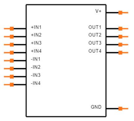
Symbol
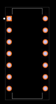
Footprint
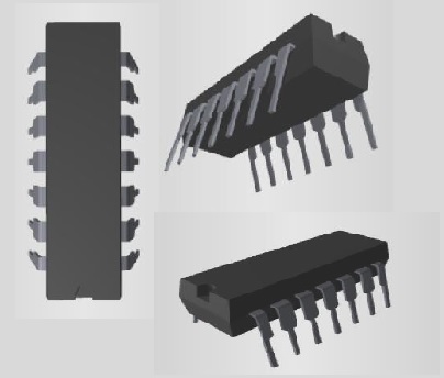
3D Models
LM339 Applications
Oscillators
Voltage comparators
Peak detectors
Logic voltage translation
Power supervision
Industrial
Measuring instruments
Automotive
LM339 Equivalents
LM339 Manufacturer
onsemi (legally ON Semiconductor Corporation; formerly ON Semiconductor until August 5, 2021) is an American semiconductor supplier company, formerly in the Fortune 500, but dropping into the Fortune 1000 (ranked 512) in 2020. Products include power and signal management, logic, discrete, and custom devices for automotive, communications, computing, consumer, industrial, LED lighting, medical, military/aerospace, and power applications. onsemi runs a network of manufacturing facilities, sales offices, and design centers in North America, Europe, and the Asia Pacific regions. Headquartered in Phoenix, Arizona, onsemi has revenues of $3.907 billion (2016), which puts it among the worldwide top 20 semiconductor sales leaders.
How to use LM339
Let's first look at the internal circuitry of four comparators in the device as shown below.
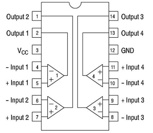
Now let's take one of the four comparators and construct a simple application circuit as shown below.
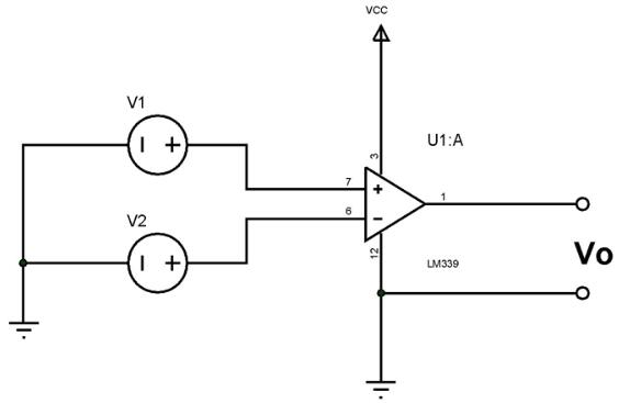
Here the comparison between the voltages V1 and V2 is performed by the device and an output is provided as Vo. Also, as shown above, the device is powered by a single voltage source of VCC.
In the circuit, the comparison output goes as,
If V1>V2 then Vo = VCC
If V2>V1 the Vo = 0V or GND
Based on the state of the output we can determine whether V1 is higher or V2 is higher at the input.
LM339 Package

LM339 vs LM339N
LM339 (Quad differential comparator) consists of four independent voltage comparators. It is a common integrated circuit and is mainly used in high-voltage digital logic gate circuits. LM339 common mode range is very large, from 0v to the power supply voltage-1.5v; wide supply voltage range: single power supply is 2-36V; dual power supply voltage is ±1V~±18V.
LM339N is a quad voltage comparator. It adopts a dual in-line 14-pin package. The maximum operating voltage is ±18V and the power consumption is 265mW. It is used in induction cookers and other products.
| LM339 | LM339N | |
| Number of channels (#) | 4 | 4 |
| Output type | Open-collector | Open-collector, Open-drain |
| Propagation delay time (µs) | 0.3 | 0.7 |
| Vs (Max) (V) | 30 | 36 |
| Vs (Min) (V) | 2 | 2 |
| Vos (offset voltage @ 25 C) (Max) (mV) | 5 | 5 |
| Iq per channel (Typ) (mA) | 0.2 | 0.2 |
| Input bias current (+/-) (Max) (nA) | 50 | 250 |
| Rail-to-rail | Out | Out |
| Operating temperature range (C) | 0 to 70 | 0 to 70 |
| Features | Standard comparator | Standard comparator |
| VICR (Max) (V) | 28.5 | 34 |
| VICR (Min) (V) | 0 | 0 |
| Approx. price (US$) | 1ku | 0.05 | 1ku | 0.24 |
How to Safely Long Run in a Circuit
For the long-term performance of the IC, it is recommended not to use the IC at its maximum ratings and always use it 20% below its maximum ratings. The IC's maximum output current is 20mA, so do not drive a load greater than 16mA. The maximum operating voltage is 36V, so do not operate the IC at more than 28V. Prevent the IC from outputting a short circuit to Vcc, as this may cause the IC to heat up and burn/damage the internal circuitry. Inputs must be below -0.3V. When operating the IC, the temperature around the IC should be below +150 degrees Celsius, and the storage temperature of the IC should be between -65 to +150 degrees Celsius.
Trend Analysis
Datasheet PDF
- PCN Obsolescence/ EOL :
- Datasheets :
- Environmental Information :
- PCN Design/Specification :
- PCN Packaging :
Parts with Similar Specs
- ImagePart NumberManufacturerPackage / CaseNumber of PinsInput Offset Voltage (Vos)Min Supply VoltageMin Dual Supply VoltageMax Supply VoltageMax Dual Supply VoltageMoisture Sensitivity Level (MSL)View Compare
![LM339N]()
LM339N
14-DIP (0.300, 7.62mm)
14
5 mV
2 V
1 V
36 V
18 V
1 (Unlimited)
![KA319]()
14-DIP (0.300, 7.62mm)
14
2 mV
-
-
-
-
1 (Unlimited)
![KA339]()
14-DIP (0.300, 7.62mm)
14
5 mV
-
-
-
-
1 (Unlimited)
![KA339A]()
DIP
14
5 mV
-
-
36 V
18 V
1 (Unlimited)
![LM339SNG]()
14-DIP (0.300, 7.62mm)
14
8 mV
15 V
-
36 V
-
1 (Unlimited)

What is LM339?
LM339 is a voltage comparator IC from the LMx39x series and is manufactured by many industries. The devices consist of four independent voltage comparators that are designed to operate from a single power supply.
What is comparator IC?
A comparator is an electronic circuit, which compares the two inputs that are applied to it and produce an output. The output value of the comparator indicates which of the inputs is greater or lesser. Please note that the comparator falls under non-linear applications of ICs.
How does LM339 comparator work?
The LM339 is a quad op amp comparator. A comparator works by a simple concept. Each op amp of a comparator has 2 inputs, an inverting input, and a noninverting input. If the inverting input voltage is greater than the noninverting input, then the output is drawn to the ground.
What is the use of LM339?
LM339 is used in applications where a comparison between two voltage signals is required. In addition with four of those comparators on board, the device can compare four pairs of voltage signals at a time which comes in handy in some applications.
Can I use LM393 instead of LM358?
The LM358 and LM393 might seem outwardly similar, but the LM358 is an operational amplifier with linear output, and the LM393 is a comparator with a digital output, and they cannot be interchanged.
 A Comprehensive Guide to LTC6911IMS-2#TRPBF Programmable Gain Instrumentation Amplifier
06 March 2024312
 A Comprehensive Guide to LTC7841EUHE#PBF DC/DC Switching Controller
06 March 2024141
 Unveiling the PIC16F610/616/16HV610/616 Microcontroller: A Detailed Exploration
29 February 2024174
 TP4056:A LiPo battery charger IC
07 March 20223712
![PMDXB950UPE 20 V dual P-channel Trench MOSFET[FAQ]](https://res.utmel.com/Images/Article/340113cd-663b-4721-83d8-46968f2d84a6.png) PMDXB950UPE 20 V dual P-channel Trench MOSFET[FAQ]
PMDXB950UPE 20 V dual P-channel Trench MOSFET[FAQ]19 April 2022535
 NC7SZ125P5X: Overview, Features, and Applications
19 December 20231121
 BMM150 Sensor: Datasheet, Pinout and Applications
27 August 20215098
 ATTINY13 8-bit AVR Microcontroller: Pinout, Equivalent and Datasheet
16 December 20214412
 What is Smoke Detector?
26 October 20213776
 What is Conductivity Sensor?
20 June 202211514
 Detailed Explanation About Twenty Kinds of Capacitor
08 November 20219152
 2026 Passive Components Market Update: Sourcing Tactics Amid Price Hikes and Lead Time Extensions
15 June 20262406
 Latest Advances in Occupancy Sensor Detection Methods
14 July 20251421
 MEMS Basics: System Features and Classifications
11 June 20217544
 Neural Processing Unit (NPU) Explained
15 October 202563894
 What is Tantalum Capacitor: Structure, Failure and Application Guide
14 April 202220778
ON Semiconductor
In Stock: 195
United States
China
Canada
Japan
Russia
Germany
United Kingdom
Singapore
Italy
Hong Kong(China)
Taiwan(China)
France
Korea
Mexico
Netherlands
Malaysia
Austria
Spain
Switzerland
Poland
Thailand
Vietnam
India
United Arab Emirates
Afghanistan
Åland Islands
Albania
Algeria
American Samoa
Andorra
Angola
Anguilla
Antigua & Barbuda
Argentina
Armenia
Aruba
Australia
Azerbaijan
Bahamas
Bahrain
Bangladesh
Barbados
Belarus
Belgium
Belize
Benin
Bermuda
Bhutan
Bolivia
Bonaire, Sint Eustatius and Saba
Bosnia & Herzegovina
Botswana
Brazil
British Indian Ocean Territory
British Virgin Islands
Brunei
Bulgaria
Burkina Faso
Burundi
Cabo Verde
Cambodia
Cameroon
Cayman Islands
Central African Republic
Chad
Chile
Christmas Island
Cocos (Keeling) Islands
Colombia
Comoros
Congo
Congo (DRC)
Cook Islands
Costa Rica
Côte d’Ivoire
Croatia
Cuba
Curaçao
Cyprus
Czechia
Denmark
Djibouti
Dominica
Dominican Republic
Ecuador
Egypt
El Salvador
Equatorial Guinea
Eritrea
Estonia
Eswatini
Ethiopia
Falkland Islands
Faroe Islands
Fiji
Finland
French Guiana
French Polynesia
Gabon
Gambia
Georgia
Ghana
Gibraltar
Greece
Greenland
Grenada
Guadeloupe
Guam
Guatemala
Guernsey
Guinea
Guinea-Bissau
Guyana
Haiti
Honduras
Hungary
Iceland
Indonesia
Iran
Iraq
Ireland
Isle of Man
Israel
Jamaica
Jersey
Jordan
Kazakhstan
Kenya
Kiribati
Kosovo
Kuwait
Kyrgyzstan
Laos
Latvia
Lebanon
Lesotho
Liberia
Libya
Liechtenstein
Lithuania
Luxembourg
Macao(China)
Madagascar
Malawi
Maldives
Mali
Malta
Marshall Islands
Martinique
Mauritania
Mauritius
Mayotte
Micronesia
Moldova
Monaco
Mongolia
Montenegro
Montserrat
Morocco
Mozambique
Myanmar
Namibia
Nauru
Nepal
New Caledonia
New Zealand
Nicaragua
Niger
Nigeria
Niue
Norfolk Island
North Korea
North Macedonia
Northern Mariana Islands
Norway
Oman
Pakistan
Palau
Palestinian Authority
Panama
Papua New Guinea
Paraguay
Peru
Philippines
Pitcairn Islands
Portugal
Puerto Rico
Qatar
Réunion
Romania
Rwanda
Samoa
San Marino
São Tomé & Príncipe
Saudi Arabia
Senegal
Serbia
Seychelles
Sierra Leone
Sint Maarten
Slovakia
Slovenia
Solomon Islands
Somalia
South Africa
South Sudan
Sri Lanka
St Helena, Ascension, Tristan da Cunha
St. Barthélemy
St. Kitts & Nevis
St. Lucia
St. Martin
St. Pierre & Miquelon
St. Vincent & Grenadines
Sudan
Suriname
Svalbard & Jan Mayen
Sweden
Syria
Tajikistan
Tanzania
Timor-Leste
Togo
Tokelau
Tonga
Trinidad & Tobago
Tunisia
Turkey
Turkmenistan
Turks & Caicos Islands
Tuvalu
U.S. Outlying Islands
U.S. Virgin Islands
Uganda
Ukraine
Uruguay
Uzbekistan
Vanuatu
Vatican City
Venezuela
Wallis & Futuna
Yemen
Zambia
Zimbabwe
![LM319MX]() LM319MX
LM319MXON Semiconductor
![LM393DR2G]() LM393DR2G
LM393DR2GON Semiconductor
![LM339DR2G]() LM339DR2G
LM339DR2GON Semiconductor
![LM239DR2G]() LM239DR2G
LM239DR2GON Semiconductor
![LM293DR2G]() LM293DR2G
LM293DR2GON Semiconductor
![LM393DMR2G]() LM393DMR2G
LM393DMR2GON Semiconductor
![LM2901DR2G]() LM2901DR2G
LM2901DR2GON Semiconductor
![LMV331SN3T1G]() LMV331SN3T1G
LMV331SN3T1GON Semiconductor
![LM2903DR2G]() LM2903DR2G
LM2903DR2GON Semiconductor
![LM2903DMR2G]() LM2903DMR2G
LM2903DMR2GON Semiconductor


