
 Product
 Brand
Brand Articles
 Tools
Tools
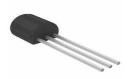
MGA-81563 Amplifier: Pinout, Equivalent and Datasheet

12.4dB PCS, PHS, ISM, SATCOM, WLL WIDE BAND LOW POWER Tape & Reel (TR) 100MHz~6GHz 2.7V~3.3V 2 P1dB:14.8dBm 2.8dB Surface Mount


12.4dB PCS, PHS, ISM, SATCOM, WLL WIDE BAND LOW POWER Tape & Reel (TR) 100MHz~6GHz 2.7V~3.3V 2 P1dB:14.8dBm 2.8dB Surface Mount
The MGA-81563 is a voltage-biased device and is designed to operate from a single, +3 volt power supply with a typical current drain of 42 mA. The internal current regulation circuit allows the amplifier to be operated with voltages as high +5 volts or as low as +1.5 volt. Furthermore, Huge range of Semiconductors, Capacitors, Resistors and IcS in stock. Welcome RFQ.

How does an Amplifier Work? (Class-A)
MGA-81563 Pinout
The following figure is the diagram of MGA-81563 Pinout.

Pinout
MGA-81563 CAD Model
The followings are MGA-81563 Symbol and Footprint.

Symbol

Footprint
MGA-81563 Description
MGA-81563 is an economical, easy-to-use GaAs MMIC amplifier that offers excellent power and low noise figure for applications from 0.1 to 6 GHz. Packaged in an ultra-miniature SOT-363 package, it requires half the board space of a SOT-143 package. The output of the amplifier is matched to 50Ω (better than 2.1:1 VSWR) across the entire bandwidth. The input is partially matched to 50Ω (better than 2.5:1 VSWR) below 4 GHz and fully matched to 50Ω (better than 2:1 VSWR) above. A simple series inductor can be added to the input to improve the input match below 4 GHz. The amplifier allows a wide dynamic range by offering a 2.7 dB NF coupled with a +27 dBm Output IP3. The circuit uses state-of-the-art PHEMT technology with proven reliability. On-chip bias circuitry allows operation from a single +3 V power supply, while resistive feedback ensures stability (K>1) over all frequencies and temperatures.
This article will introduce MGA-81563 systematically from its features, pinout to its specifications, applications, also including MGA-81563 datasheet and so much more.
MGA-81563 Features
● Lead-free Option Available
● +14.8 dBm P1dB at 2.0 GHz; +17 dBm Psat at 2.0 GHz
● Single +3V Supply
● 2.8 dB Noise Figure at 2.0 GHz
● 12.4 dB Gain at 2.0 GHz
● Ultra-miniature Package
● Unconditionally Stable
Specifications
- TypeParameter
- Mounting Type
The "Mounting Type" in electronic components refers to the method used to attach or connect a component to a circuit board or other substrate, such as through-hole, surface-mount, or panel mount.
Surface Mount - Package / Case
refers to the protective housing that encases an electronic component, providing mechanical support, electrical connections, and thermal management.
6-TSSOP, SC-88, SOT-363 - Surface Mount
having leads that are designed to be soldered on the side of a circuit board that the body of the component is mounted on.
YES - Operating Temperature (Max.)85°C
- Operating Temperature (Min.)-40°C
- Packaging
Semiconductor package is a carrier / shell used to contain and cover one or more semiconductor components or integrated circuits. The material of the shell can be metal, plastic, glass or ceramic.
Tape & Reel (TR) - Published2005
- JESD-609 Code
The "JESD-609 Code" in electronic components refers to a standardized marking code that indicates the lead-free solder composition and finish of electronic components for compliance with environmental regulations.
e0 - Part Status
Parts can have many statuses as they progress through the configuration, analysis, review, and approval stages.
Obsolete - Moisture Sensitivity Level (MSL)
Moisture Sensitivity Level (MSL) is a standardized rating that indicates the susceptibility of electronic components, particularly semiconductors, to moisture-induced damage during storage and the soldering process, defining the allowable exposure time to ambient conditions before they require special handling or baking to prevent failures
1 (Unlimited) - Number of Terminations6
- ECCN Code
An ECCN (Export Control Classification Number) is an alphanumeric code used by the U.S. Bureau of Industry and Security to identify and categorize electronic components and other dual-use items that may require an export license based on their technical characteristics and potential for military use.
5A991.G - Terminal Finish
Terminal Finish refers to the surface treatment applied to the terminals or leads of electronic components to enhance their performance and longevity. It can improve solderability, corrosion resistance, and overall reliability of the connection in electronic assemblies. Common finishes include nickel, gold, and tin, each possessing distinct properties suitable for various applications. The choice of terminal finish can significantly impact the durability and effectiveness of electronic devices.
Tin/Lead (Sn/Pb) - Additional Feature
Any Feature, including a modified Existing Feature, that is not an Existing Feature.
LOW NOISE, HIGH RELIABILITY - HTS Code
HTS (Harmonized Tariff Schedule) codes are product classification codes between 8-1 digits. The first six digits are an HS code, and the countries of import assign the subsequent digits to provide additional classification. U.S. HTS codes are 1 digits and are administered by the U.S. International Trade Commission.
8542.33.00.01 - Voltage - Supply
Voltage - Supply refers to the range of voltage levels that an electronic component or circuit is designed to operate with. It indicates the minimum and maximum supply voltage that can be applied for the device to function properly. Providing supply voltages outside this range can lead to malfunction, damage, or reduced performance. This parameter is critical for ensuring compatibility between different components in a circuit.
2.7V~3.3V - Number of Functions1
- Construction
Construction in electronic components refers to the design and materials used in the manufacturing of the components. It encompasses the physical structure, arrangement, and integration of various parts like substrates, conductors, and insulators. The construction impacts the performance, reliability, and thermal properties of the component, influencing how it interacts with electrical signals and other components in a circuit. Different construction techniques can also affect the size, weight, and cost of the electronic component.
COMPONENT - Frequency
In electronic components, the parameter "Frequency" refers to the rate at which a signal oscillates or cycles within a given period of time. It is typically measured in Hertz (Hz) and represents how many times a signal completes a full cycle in one second. Frequency is a crucial aspect in electronic components as it determines the behavior and performance of various devices such as oscillators, filters, and communication systems. Understanding the frequency characteristics of components is essential for designing and analyzing electronic circuits to ensure proper functionality and compatibility with other components in a system.
100MHz~6GHz - Power Supplies
an electronic circuit that converts the voltage of an alternating current (AC) into a direct current (DC) voltage.?
3V - Test Frequency
a statistical procedure for assessing data that contain counts or the numbers of occurrences of various categories or classes.
2GHz - Current - Supply
Current - Supply is a parameter in electronic components that refers to the maximum amount of electrical current that the component can provide to the circuit it is connected to. It is typically measured in units of amperes (A) and is crucial for determining the power handling capability of the component. Understanding the current supply rating is important for ensuring that the component can safely deliver the required current without overheating or failing. It is essential to consider this parameter when designing circuits to prevent damage to the component and ensure proper functionality of the overall system.
51mA - Gain
In electronic components, "Gain" refers to the ratio of the output signal amplitude to the input signal amplitude. It is a measure of the amplification provided by the component, such as a transistor or operational amplifier. Gain is typically expressed in decibels (dB) or as a numerical value, indicating how much the signal is amplified by the component.A higher gain value indicates a greater amplification of the input signal, while a lower gain value indicates less amplification. Gain is an important parameter in designing and analyzing electronic circuits, as it determines the overall performance and functionality of the system. Different components have different gain characteristics, and understanding the gain of a component is crucial for achieving the desired signal processing or amplification in electronic systems.
12.4dB - RF/Microwave Device Type
The parameter "RF/Microwave Device Type" in electronic components refers to the specific type or category of devices designed to operate within the radio frequency (RF) and microwave frequency ranges. These devices are engineered to handle high-frequency signals and are commonly used in various applications such as wireless communication, radar systems, satellite communication, and more. Examples of RF/Microwave device types include amplifiers, filters, mixers, oscillators, antennas, and transceivers. Understanding the RF/Microwave device type is crucial for selecting the appropriate component that meets the requirements of a particular RF system or application.
WIDE BAND LOW POWER - VSWR-Max
VSWR-Max stands for Voltage Standing Wave Ratio Maximum, which is a parameter used in electronic components, particularly in RF and microwave applications. It measures how effectively power is transmitted from a source through a transmission line to a load, indicating the level of reflected power due to impedance mismatches. A lower VSWR-Max value signifies better impedance matching and higher efficiency, while a higher value indicates poor matching, leading to greater signal reflections and potential performance issues. Manufacturers specify VSWR-Max to help ensure components operate within acceptable limits for optimal functionality.
2 - RF Type
The rate of oscillation of electromagnetic radio waves in the range of 3 kHz to 3 GHz, as well as the alternating currents carrying the radio signals.
PCS, PHS, ISM, SATCOM, WLL - Input Power-Max (CW)
Input Power-Max (CW) is a parameter used to specify the maximum continuous wave power that an electronic component can handle without being damaged. This parameter is crucial in determining the power handling capability of the component under continuous wave operation. It is typically measured in watts and provides important information for designing circuits and systems to ensure that the component operates within its safe power limits. Exceeding the specified Input Power-Max (CW) can lead to overheating, degradation, or even permanent damage to the component.
13dBm - Characteristic Impedance
Characteristic impedance is a fundamental property of transmission lines and refers to the specific impedance that a transmission line presents to an electrical wave propagating along it. It is determined by the physical parameters of the transmission line, including its inductance and capacitance per unit length. When the line is terminated with a load that matches its characteristic impedance, maximum power transfer occurs, minimizing reflections and signal losses. In high-frequency applications, maintaining the characteristic impedance is crucial for signal integrity and performance.
50Ohm - Noise Figure
Noise figure (NF) and noise factor (F) are measures of degradation of the signal-to-noise ratio (SNR), caused by components in a signal chain.
2.8dB - P1dB
P1dB, or the 1-dB compression point, is a key parameter in electronic components, particularly in amplifiers and RF (radio frequency) devices. It indicates the output power level at which the gain of the device starts to decrease by 1 dB relative to the expected linear gain. At this point, the device is nearing saturation, and its ability to linearly amplify signals diminishes. Understanding P1dB is essential for designers to ensure that devices operate effectively within their linear region under typical operating conditions.
14.8dBm - RoHS Status
RoHS means “Restriction of Certain Hazardous Substances” in the “Hazardous Substances Directive” in electrical and electronic equipment.
Non-RoHS Compliant
MGA-81563 Functional Block Diagram
The following figure is the diagram of MGA-81563 Simplified Schematic.

Simplified Schematic
MGA-81563 Equivalent
| Model number | Manufacturer | Description |
| MGA-81563-TR1G | Avago Technologies | 100MHz - 6000MHz RF/MICROWAVE WIDE BAND LOW POWER AMPLIFIER, LEAD FREE, ULTRA MINI, SC-70, SOT-363, 4 PIN |
| MGA-81563-BLK | Agilent Technologies Inc | Wide Band Low Power Amplifier, 100MHz Min, 6000MHz Max, GAAS, SC-70, SOT-363, 6 PIN |
| MGA-81563-BLKG | Avago Technologies | 100MHz - 6000MHz RF/MICROWAVE WIDE BAND LOW POWER AMPLIFIER, LEAD FREE, ULTRA MINI, SC-70, SOT-363, 4 PIN |
| MGA-81563-TR1 | Agilent Technologies Inc | Wide Band Low Power Amplifier, 100MHz Min, 6000MHz Max, GAAS, SC-70, SOT-363, 6 PIN |
MGA-81563 Applications
● Buffer or Driver Amp for PCS, PHS, ISM, SATCOM and WLL Applications
● High Dynamic Range LNA
MGA-81563 Package
The following diagrams show the MGA-81563 Package.

View A

View B

View C
MGA-81563 Manufacturer
Broadcom Limited is a diversified global semiconductor leader built on 50 years of innovation, collaboration and engineering excellence.Broadcom's extensive product portfolio serves multiple applications within four primary end markets: wired infrastructure, wireless communications, enterprise storage and industrial & others. Applications for our products in these end markets include: data center networking, home connectivity, broadband access, telecommunications equipment, smartphones and base stations, data center servers and storage, factory automation, power generation and alternative energy systems, and displays.
Datasheet PDF
- Datasheets :
How many pins of MGA-81563-TR1?
6 Pins.
What’s the operating temperature of MGA-81563-TR1?
-40°C~85°C TA.
What is the essential property of the MGA-81563?
The MGA-81563 is a voltage-biased device and is designed to operate from a single, +3 volt power supply with a typical current drain of 42 mA. The internal current regulation circuit allows the amplifier to be operated with voltages as high +5 volts or as low as +1.5 volt.
 TDA7498E Audio Amplifier: Block Diagram, Datasheet, and Test Circuit
13 July 202122234
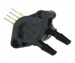 MPX2010DP Pressure Sensor: MPX2010DP Datasheet and Block Diagram
28 March 20224455
 TDA2040 Hi-Fi Audio Power Amplifier: Replacement, Circuit and Datasheet
28 October 20216900
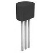 MPSA56 Transistor: MPSA56, Equivalent, Datasheet
07 January 20229853
 BF246 N-Channel Switch: Pinout, Datasheet, Equivalent
27 April 20222570
 STM32H743XIH6 Review: High-Performance 480MHz ARM Cortex-M7 Microcontroller Comparison Guide
24 July 20256609
 PIC12C5XX Series: 8-Pin 8-Bit CMOS Microcontrollers Overview
28 February 2024197
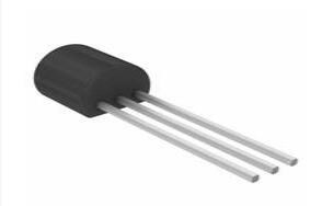
 2N5484 Transistor: 2N5484 Datasheet, Pinout, Equivalent
21 February 20222861
 Reverse Voltage Protection for Battery Chargers
29 March 20225608
 What Are Wi-Fi Modules and Their Uses in IoT Today
04 June 20253136
 How to Increase Laptop Battery Life
03 July 20213480
 What is a DC-to-DC Converter?
23 April 20217485
 Understanding Electronic Speed Controllers (ESCs): Working Principles, Key Specifications, and Sourcing Guide
15 June 2026393
 Organic Semiconductor Market Set to Reach USD 843.62 Billion by 2032, Driven by Rising Demand for Flexible Electronics
05 October 20232539
 Exploring the Advancements in Storage Technologies and Grid Architecture of Electric Vehicle Charging Systems
18 October 20232516
 Semiconductor Market Expected to Surge, Driven by Rising Number of Data Centers
04 June 20242852
Broadcom Limited
In Stock
United States
China
Canada
Japan
Russia
Germany
United Kingdom
Singapore
Italy
Hong Kong(China)
Taiwan(China)
France
Korea
Mexico
Netherlands
Malaysia
Austria
Spain
Switzerland
Poland
Thailand
Vietnam
India
United Arab Emirates
Afghanistan
Åland Islands
Albania
Algeria
American Samoa
Andorra
Angola
Anguilla
Antigua & Barbuda
Argentina
Armenia
Aruba
Australia
Azerbaijan
Bahamas
Bahrain
Bangladesh
Barbados
Belarus
Belgium
Belize
Benin
Bermuda
Bhutan
Bolivia
Bonaire, Sint Eustatius and Saba
Bosnia & Herzegovina
Botswana
Brazil
British Indian Ocean Territory
British Virgin Islands
Brunei
Bulgaria
Burkina Faso
Burundi
Cabo Verde
Cambodia
Cameroon
Cayman Islands
Central African Republic
Chad
Chile
Christmas Island
Cocos (Keeling) Islands
Colombia
Comoros
Congo
Congo (DRC)
Cook Islands
Costa Rica
Côte d’Ivoire
Croatia
Cuba
Curaçao
Cyprus
Czechia
Denmark
Djibouti
Dominica
Dominican Republic
Ecuador
Egypt
El Salvador
Equatorial Guinea
Eritrea
Estonia
Eswatini
Ethiopia
Falkland Islands
Faroe Islands
Fiji
Finland
French Guiana
French Polynesia
Gabon
Gambia
Georgia
Ghana
Gibraltar
Greece
Greenland
Grenada
Guadeloupe
Guam
Guatemala
Guernsey
Guinea
Guinea-Bissau
Guyana
Haiti
Honduras
Hungary
Iceland
Indonesia
Iran
Iraq
Ireland
Isle of Man
Israel
Jamaica
Jersey
Jordan
Kazakhstan
Kenya
Kiribati
Kosovo
Kuwait
Kyrgyzstan
Laos
Latvia
Lebanon
Lesotho
Liberia
Libya
Liechtenstein
Lithuania
Luxembourg
Macao(China)
Madagascar
Malawi
Maldives
Mali
Malta
Marshall Islands
Martinique
Mauritania
Mauritius
Mayotte
Micronesia
Moldova
Monaco
Mongolia
Montenegro
Montserrat
Morocco
Mozambique
Myanmar
Namibia
Nauru
Nepal
New Caledonia
New Zealand
Nicaragua
Niger
Nigeria
Niue
Norfolk Island
North Korea
North Macedonia
Northern Mariana Islands
Norway
Oman
Pakistan
Palau
Palestinian Authority
Panama
Papua New Guinea
Paraguay
Peru
Philippines
Pitcairn Islands
Portugal
Puerto Rico
Qatar
Réunion
Romania
Rwanda
Samoa
San Marino
São Tomé & Príncipe
Saudi Arabia
Senegal
Serbia
Seychelles
Sierra Leone
Sint Maarten
Slovakia
Slovenia
Solomon Islands
Somalia
South Africa
South Sudan
Sri Lanka
St Helena, Ascension, Tristan da Cunha
St. Barthélemy
St. Kitts & Nevis
St. Lucia
St. Martin
St. Pierre & Miquelon
St. Vincent & Grenadines
Sudan
Suriname
Svalbard & Jan Mayen
Sweden
Syria
Tajikistan
Tanzania
Timor-Leste
Togo
Tokelau
Tonga
Trinidad & Tobago
Tunisia
Turkey
Turkmenistan
Turks & Caicos Islands
Tuvalu
U.S. Outlying Islands
U.S. Virgin Islands
Uganda
Ukraine
Uruguay
Uzbekistan
Vanuatu
Vatican City
Venezuela
Wallis & Futuna
Yemen
Zambia
Zimbabwe
![MGA-62563-TR1G]() MGA-62563-TR1G
MGA-62563-TR1GBroadcom Limited
![MGA-22003-BLKG]() MGA-22003-BLKG
MGA-22003-BLKGBroadcom Limited
![ADA-4643-BLKG]() ADA-4643-BLKG
ADA-4643-BLKGBroadcom Limited
![MGA-31389-BLKG]() MGA-31389-BLKG
MGA-31389-BLKGBroadcom Limited
![MGA-631P8-TR1G]() MGA-631P8-TR1G
MGA-631P8-TR1GBroadcom Limited
![ALM-2812-BLKG]() ALM-2812-BLKG
ALM-2812-BLKGBroadcom Limited
![MGA-30989-TR1G]() MGA-30989-TR1G
MGA-30989-TR1GBroadcom Limited
![ABA-52563-BLKG]() ABA-52563-BLKG
ABA-52563-BLKGBroadcom Limited
![MGA-31689-BLKG]() MGA-31689-BLKG
MGA-31689-BLKGBroadcom Limited
![MGA-68563-TR1G]() MGA-68563-TR1G
MGA-68563-TR1GBroadcom Limited


