

 Product
 Brand
Brand Articles
 Tools
Tools
SN75176BP Transceiver: Circuit, Pinout, and Datasheet [Video&FAQ]


8 Terminations 8 Pin SN75176 Receivers 1 Bits 1/1 Drivers/Receivers 1 Functions
The SN75176BP differential bus transceiver is a monolithic integrated circuit designed for two-way data communication on a multipoint bus transmission line. This article mainly introduces circuit, pinout, datasheet and other detailed information about Texas Instruments SN75176BP.

SN75176BP Differential Bus Transceivers
- SN75176BP Description
- SN75176BP Pinout
- SN75176BP CAD Model
- SN75176BP Features
- Specifications
- Parts with Similar Specs
- SN75176BP Typical Application Circuit
- SN75176BP Logic Symbol
- SN75176BP Logic Diagram
- SN75176BP Equivalent Of Each Input
- SN75176BP Typical Of Receiver Output
- SN75176BP Layout
- SN75176BP Alternatives
- SN75176BP Applications
- SN75176BP Package
- SN75176BP Manufacturer
- Trend Analysis
- Datasheet PDF
SN75176BP Description
The SN75176BP differential bus transceiver is a monolithic integrated circuit designed for two-way data communication on a multipoint bus transmission line. It is specially designed for balanced transmission lines and complies with ANSI standard EIA/TIA-422-B and ITU recommendation V.11.
SN75176BP combines a three-state differential line driver and a differential input line receiver, both of which are powered by a single 5V power supply. The driver and the receiver have high-level active and low-level active enable respectively, and they can be connected together externally for direction control. The driver differential output and receiver differential input are connected internally to form a differential input/output (I/O) bus port designed to provide a minimum load on the bus when the driver is disabled or VCC = 0. These ports have a wide positive and negative common-mode voltage range making the device suitable for party-line applications.
The driver is designed to handle loads that sink or source currents up to 60 mA. The driver has positive and negative current limiting and thermal shutdown functions to provide protection in the event of a line fault. Thermal shutdown is designed to occur at a junction temperature of approximately 150°C. The receiver has a minimum input impedance of 12 kΩ, input sensitivity of ±200 mV, and a typical input hysteresis of 50 mV.
SN75176BP can be used in transmission line applications using SN75172 and SN75174 quad differential line drivers and SN75173 and SN75175 quad differential line receivers. The interface type of SN75176BP is RS-485 /RS-422, the operating temperature range is 0°C to +70°C, and the package type is DIP.
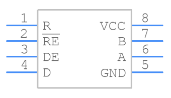
SN75176BP Pinout
The following figure is the SN75176BP Pinout.

Pinout
SN75176BP CAD Model
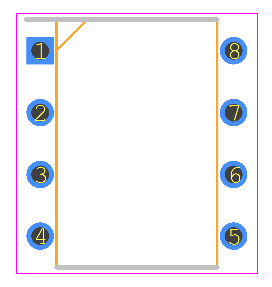

SN75176BP Features
● Bidirectional Transceiver
● Meets Or Exceeds The Requirements Of ANSI Standards EIA/TIA-422-B And ITU Recommendation V.11
● Designed For Multipoint Transmission On Long Bus Lines In Noisy Environments
● 3-State Driver And Receiver Outputs
● Individual Driver And Receiver Enables
● Wide Positive And Negative Input/Output Bus Voltage Ranges
● Driver Output Capability... ±60 mA Max
● Thermal-Shutdown Protection
● Driver Positive And Negative-Current Limiting
● Receiver Input Impedance . . . 12 kΩ Min
● Receiver Input Sensitivity... ±200 mV
● Receiver Input Hysteresis . . . 50 mV Typ
● Operates From Single 5-V Supply
● Low Power Requirements
Specifications
- TypeParameter
- Factory Lead Time12 Weeks
- Contact Plating
Contact plating (finish) provides corrosion protection for base metals and optimizes the mechanical and electrical properties of the contact interfaces.
Gold - Mount
In electronic components, the term "Mount" typically refers to the method or process of physically attaching or fixing a component onto a circuit board or other electronic device. This can involve soldering, adhesive bonding, or other techniques to secure the component in place. The mounting process is crucial for ensuring proper electrical connections and mechanical stability within the electronic system. Different components may have specific mounting requirements based on their size, shape, and function, and manufacturers provide guidelines for proper mounting procedures to ensure optimal performance and reliability of the electronic device.
Through Hole - Mounting Type
The "Mounting Type" in electronic components refers to the method used to attach or connect a component to a circuit board or other substrate, such as through-hole, surface-mount, or panel mount.
Through Hole - Package / Case
refers to the protective housing that encases an electronic component, providing mechanical support, electrical connections, and thermal management.
8-DIP (0.300, 7.62mm) - Number of Pins8
- Weight440.409842mg
- Current - Supply (Nom)70mA
- Operating Temperature
The operating temperature is the range of ambient temperature within which a power supply, or any other electrical equipment, operate in. This ranges from a minimum operating temperature, to a peak or maximum operating temperature, outside which, the power supply may fail.
0°C~70°C - Packaging
Semiconductor package is a carrier / shell used to contain and cover one or more semiconductor components or integrated circuits. The material of the shell can be metal, plastic, glass or ceramic.
Tube - JESD-609 Code
The "JESD-609 Code" in electronic components refers to a standardized marking code that indicates the lead-free solder composition and finish of electronic components for compliance with environmental regulations.
e4 - Pbfree Code
The "Pbfree Code" parameter in electronic components refers to the code or marking used to indicate that the component is lead-free. Lead (Pb) is a toxic substance that has been widely used in electronic components for many years, but due to environmental concerns, there has been a shift towards lead-free alternatives. The Pbfree Code helps manufacturers and users easily identify components that do not contain lead, ensuring compliance with regulations and promoting environmentally friendly practices. It is important to pay attention to the Pbfree Code when selecting electronic components to ensure they meet the necessary requirements for lead-free applications.
yes - Part Status
Parts can have many statuses as they progress through the configuration, analysis, review, and approval stages.
ACTIVE (Last Updated: 4 days ago) - Moisture Sensitivity Level (MSL)
Moisture Sensitivity Level (MSL) is a standardized rating that indicates the susceptibility of electronic components, particularly semiconductors, to moisture-induced damage during storage and the soldering process, defining the allowable exposure time to ambient conditions before they require special handling or baking to prevent failures
1 (Unlimited) - Number of Terminations8
- ECCN Code
An ECCN (Export Control Classification Number) is an alphanumeric code used by the U.S. Bureau of Industry and Security to identify and categorize electronic components and other dual-use items that may require an export license based on their technical characteristics and potential for military use.
EAR99 - TypeTransceiver
- Voltage - Supply
Voltage - Supply refers to the range of voltage levels that an electronic component or circuit is designed to operate with. It indicates the minimum and maximum supply voltage that can be applied for the device to function properly. Providing supply voltages outside this range can lead to malfunction, damage, or reduced performance. This parameter is critical for ensuring compatibility between different components in a circuit.
5V - Terminal Position
In electronic components, the term "Terminal Position" refers to the physical location of the connection points on the component where external electrical connections can be made. These connection points, known as terminals, are typically used to attach wires, leads, or other components to the main body of the electronic component. The terminal position is important for ensuring proper connectivity and functionality of the component within a circuit. It is often specified in technical datasheets or component specifications to help designers and engineers understand how to properly integrate the component into their circuit designs.
DUAL - Number of Functions1
- Terminal Pitch
The center distance from one pole to the next.
2.54mm - Base Part Number
The "Base Part Number" (BPN) in electronic components serves a similar purpose to the "Base Product Number." It refers to the primary identifier for a component that captures the essential characteristics shared by a group of similar components. The BPN provides a fundamental way to reference a family or series of components without specifying all the variations and specific details.
SN75176 - Current - Supply (Max)
The parameter "Current - Supply (Max)" in electronic components refers to the maximum amount of current that a component can draw from a power supply for its operation. This parameter is critical for ensuring that the power supply can adequately meet the demands of the component without causing damage or malfunction. Exceeding this specified maximum current can lead to overheating, reduced performance, or failure of the component. It is essential to consider this value when designing or integrating components into electronic circuits to maintain reliability and functionality.
70mA - Power Supplies
an electronic circuit that converts the voltage of an alternating current (AC) into a direct current (DC) voltage.?
5V - Output Current
The rated output current is the maximum load current that a power supply can provide at a specified ambient temperature. A power supply can never provide more current that it's rated output current unless there is a fault, such as short circuit at the load.
60mA - Current - Supply
Current - Supply is a parameter in electronic components that refers to the maximum amount of electrical current that the component can provide to the circuit it is connected to. It is typically measured in units of amperes (A) and is crucial for determining the power handling capability of the component. Understanding the current supply rating is important for ensuring that the component can safely deliver the required current without overheating or failing. It is essential to consider this parameter when designing circuits to prevent damage to the component and ensure proper functionality of the overall system.
70mA - Data Rate
Data Rate is defined as the amount of data transmitted during a specified time period over a network. It is the speed at which data is transferred from one device to another or between a peripheral device and the computer. It is generally measured in Mega bits per second(Mbps) or Mega bytes per second(MBps).
10 Mbps - Output Characteristics
Output characteristics in electronic components refer to the relationship between the output voltage and output current across a range of input conditions. This parameter is essential for understanding how a device, such as a transistor or operational amplifier, behaves under various loads and operating points. It provides insights into the efficiency, performance, and limitations of the component, helping designers to make informed choices for circuits and applications.
3-STATE - Differential Output
a differential output voltage in electronics is the difference between the values of two AC voltages, 180° out of phase, present at the output terminals of an amplifier when you apply a differential input voltage to the input terminals of an amplifier.
Yes - Nominal Input Voltage
The actual voltage at which a circuit operates can vary from the nominal voltage within a range that permits satisfactory operation of equipment. The word “nominal” means “named”.
2V - Output Polarity
Output polarity in electronic components refers to the orientation of the output signal in relation to the ground or reference voltage. It indicates whether the output voltage is positive or negative with respect to the ground. Positive output polarity means the signal is higher than the ground potential, while negative output polarity signifies that the signal is lower than the ground. This characteristic is crucial for determining compatibility with other components in a circuit and ensuring proper signal processing.
COMPLEMENTARY - Protocol
In electronic components, the parameter "Protocol" refers to a set of rules and standards that govern the communication between devices. It defines the format, timing, sequencing, and error checking methods for data exchange between different components or systems. Protocols ensure that devices can understand and interpret data correctly, enabling them to communicate effectively with each other. Common examples of protocols in electronics include USB, Ethernet, SPI, I2C, and Bluetooth, each with its own specifications for data transmission. Understanding and adhering to protocols is essential for ensuring compatibility and reliable communication between electronic devices.
RS422, RS485 - Input Characteristics
In electronic components, "Input Characteristics" refer to the set of specifications that describe how the component behaves in response to signals or inputs applied to it. These characteristics typically include parameters such as input voltage, input current, input impedance, input capacitance, and input frequency range. Understanding the input characteristics of a component is crucial for designing circuits and systems, as it helps ensure compatibility and proper functioning. By analyzing these parameters, engineers can determine how the component will interact with the signals it receives and make informed decisions about its use in a particular application.
DIFFERENTIAL SCHMITT TRIGGER - Number of Drivers/Receivers1/1
- Driver Number of Bits1
- Receiver Number of Bits1
- Duplex
In the context of electronic components, "Duplex" refers to a type of communication system that allows for bidirectional data flow. It enables two devices to communicate with each other simultaneously, allowing for both sending and receiving of data at the same time. Duplex communication can be further categorized into two types: half-duplex, where data can be transmitted in both directions but not at the same time, and full-duplex, where data can be sent and received simultaneously. This parameter is crucial in networking and telecommunications systems to ensure efficient and effective data transmission between devices.
Half - Receiver Hysteresis
Receiver hysteresis is?commonly used to ensure glitch-free reception even when differential noise is present. This application report compares the noise immunity of the SN65HVD37 to similar devices available from competitors. Contents.
50mV - Number of Transceivers1
- ESD Protection
ESD protection, or Electrostatic Discharge protection, is a feature in electronic components designed to prevent damage caused by sudden electrostatic discharges. These discharges can occur when a person or object with an electric charge comes into contact with a sensitive electronic component, leading to a rapid flow of static electricity that can damage or destroy the component. ESD protection mechanisms in electronic components typically involve the use of special materials or circuitry that can safely dissipate or divert the excess charge away from the sensitive components, thus safeguarding the device from potential harm. Implementing effective ESD protection is crucial in ensuring the reliability and longevity of electronic devices, especially in environments where static electricity buildup is common, such as in manufacturing facilities or areas with low humidity.
No - Receive Delay-Max
Receive Delay-Max is a parameter in electronic components that refers to the maximum amount of time it takes for a device to receive and process incoming signals or data after they have been transmitted. This parameter is crucial in determining the overall performance and efficiency of the component, especially in applications where timing is critical. A lower Receive Delay-Max value indicates faster response times and better overall performance, while a higher value may result in delays and potential issues in data transmission. It is important to consider and optimize the Receive Delay-Max parameter when designing or selecting electronic components for specific applications to ensure reliable and efficient operation.
35 ns - Simplex/Duplex
In electronic components, the parameter "Simplex/Duplex" refers to the type of communication or data transmission mode supported by the component. Simplex communication is a one-way communication mode where data flows only in one direction, from the sender to the receiver. This means that the sender can only transmit data, and the receiver can only receive data. On the other hand, duplex communication is a two-way communication mode where data can flow in both directions, allowing for simultaneous transmission and reception of data between two devices. Understanding whether a component supports simplex or duplex communication is important for determining how data will be exchanged between devices and ensuring compatibility in a given system.
Half Duplex - Transmit Delay-Max
Transmit Delay-Max refers to the maximum time interval it takes for a signal to be transmitted from the input to the output of an electronic component or system. This parameter is critical in digital circuits and communication systems, as it affects the overall performance and timing of data transmission. A lower Transmit Delay-Max indicates faster signal propagation, which is essential for high-speed applications. It is typically specified in nanoseconds or microseconds, depending on the technology and design of the component.
22 ns - Supply Voltage1-Nom
Supply Voltage1-Nom is a parameter in electronic components that refers to the nominal or rated voltage level at which the component is designed to operate optimally. This parameter specifies the voltage level that the component requires to function correctly and efficiently. It is important to ensure that the actual supply voltage provided to the component closely matches the specified nominal voltage to prevent damage or malfunction. Deviating significantly from the nominal voltage may result in unreliable performance or even permanent damage to the component. It is crucial to adhere to the specified supply voltage range to ensure the proper functioning and longevity of the electronic component.
5V - Output Low Current-Max
Output Low Current-Max is a parameter in electronic components that specifies the maximum amount of current that can flow out of the output pin when it is in a low state. This parameter is important for determining the capability of the component to sink current when driving external loads. It is typically measured in units of amperes (A) and helps in ensuring that the component can effectively drive connected devices without being damaged. Designers use this parameter to ensure proper functioning and reliability of the overall circuit by selecting components with appropriate output low current-max ratings.
0.00002A - High Level Input Current-Max
High Level Input Current-Max is a parameter in electronic components that specifies the maximum current that can be safely input to the device when the input signal is at a high logic level. This parameter is important for ensuring that the component operates within its specified limits and does not get damaged due to excessive current flow. It is typically measured in milliamperes (mA) and helps in determining the compatibility of the component with the input signal source. Designers and engineers use this parameter to select components that can handle the expected input current levels without malfunctioning.
0.00002A - Height5.08mm
- Length9.81mm
- Width6.35mm
- Thickness
Thickness in electronic components refers to the measurement of how thick a particular material or layer is within the component structure. It can pertain to various aspects, such as the thickness of a substrate, a dielectric layer, or conductive traces. This parameter is crucial as it impacts the electrical, mechanical, and thermal properties of the component, influencing its performance and reliability in electronic circuits.
3.9mm - REACH SVHC
The parameter "REACH SVHC" in electronic components refers to the compliance with the Registration, Evaluation, Authorization, and Restriction of Chemicals (REACH) regulation regarding Substances of Very High Concern (SVHC). SVHCs are substances that may have serious effects on human health or the environment, and their use is regulated under REACH to ensure their safe handling and minimize their impact.Manufacturers of electronic components need to declare if their products contain any SVHCs above a certain threshold concentration and provide information on the safe use of these substances. This information allows customers to make informed decisions about the potential risks associated with using the components and take appropriate measures to mitigate any hazards.Ensuring compliance with REACH SVHC requirements is essential for electronics manufacturers to meet regulatory standards, protect human health and the environment, and maintain transparency in their supply chain. It also demonstrates a commitment to sustainability and responsible manufacturing practices in the electronics industry.
No SVHC - RoHS Status
RoHS means “Restriction of Certain Hazardous Substances” in the “Hazardous Substances Directive” in electrical and electronic equipment.
ROHS3 Compliant - Lead Free
Lead Free is a term used to describe electronic components that do not contain lead as part of their composition. Lead is a toxic material that can have harmful effects on human health and the environment, so the electronics industry has been moving towards lead-free components to reduce these risks. Lead-free components are typically made using alternative materials such as silver, copper, and tin. Manufacturers must comply with regulations such as the Restriction of Hazardous Substances (RoHS) directive to ensure that their products are lead-free and environmentally friendly.
Lead Free
Parts with Similar Specs
- ImagePart NumberManufacturerPackage / CaseNumber of PinsDriver Number of BitsReceiver Number of BitsData RateSimplex/DuplexSupply VoltageSupply Voltage1-NomView Compare
![SN75176BP]()
SN75176BP
8-DIP (0.300, 7.62mm)
8
1
1
10 Mbps
Half Duplex
5 V
5 V
![SN75176AP]()
8-DIP (0.300, 7.62mm)
8
1
1
10 Mbps
Half Duplex
5 V
5 V
![TL3695P]()
8-DIP (0.300, 7.62mm)
8
1
-
10 Mbps
Half Duplex
5 V
5 V

SN75176BP Typical Application Circuit
The following figure is the Typical Application Circuit of SN75176BP.
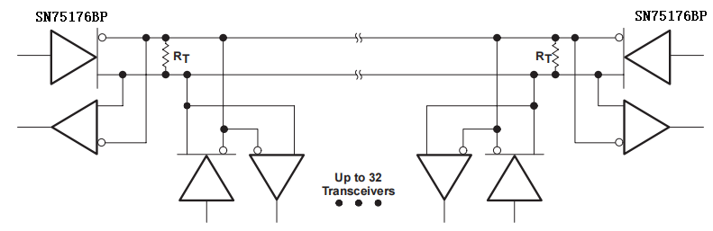
Typical Application Circuit
SN75176BP Logic Symbol
The following figure is the Logic Symbol of SN75176BP.
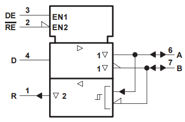
Logic Symbol
SN75176BP Logic Diagram
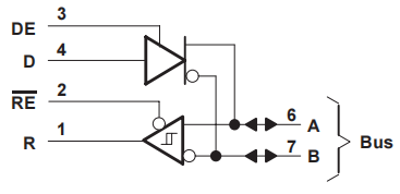
SN75176BP Equivalent Of Each Input
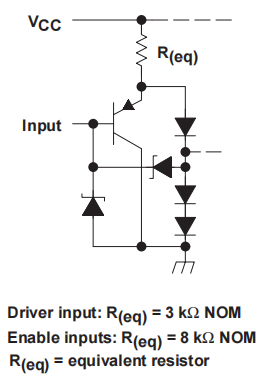
Equivalent Of Each Input
SN75176BP Typical Of Receiver Output
The following figure is the SN75176BP Typical Of Receiver Output.
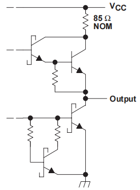
Typical Of Receiver Output
SN75176BP Layout
The following figure is the SN75176BP Layout.
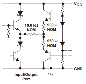
Layout
SN75176BP Alternatives
| Part Number | Description | Manufacturer |
| DS16F95JFQMLVDRIVERS AND INTERFACES | LINE TRANSCEIVER, CDIP8, CERDIP-8 | Texas Instruments |
| SP1485ECPDRIVERS AND INTERFACES | Line Transceiver, 1 Func, 1 Driver, 1 Rcvr, BICMOS, PDIP8, PLASTIC, DIP-8 | Sipex Corporation |
| SN75176BJG-00DRIVERS AND INTERFACES | LINE TRANSCEIVER, CDIP8, 0.300 INCH, HERMETIC SEALED, CERAMIC, DIP-8 | Texas Instruments |
| DS75176BTN/NOPBDRIVERS AND INTERFACES | IC LINE TRANSCEIVER, PDIP8, PLASTIC, DIP-8, Line Driver or Receiver | National Semiconductor Corporation |
| DS16F95J/883DRIVERS AND INTERFACES | IC LINE TRANSCEIVER, CDIP8, CERAMIC, DIP-8, Line Driver or Receiver | National Semiconductor Corporation |
SN75176BP Applications
● Transmission Lines
● Party Line Applications
● Provide Protection In The Event Of A Line Fault
● Be Used In Transmission Line Applications Using SN75172 And SN75174 Quad Differential Line Drivers And SN75173 And SN75175 Quad Differential Line Receivers
SN75176BP Package

Package
SN75176BP Manufacturer
Texas Instruments (TI) became a globally recognized semiconductor manufacturer and expanded its business to 35 countries/regions. It has seen rapid growth. In 1958, TIer first introduced a working integrated circuit.
Today, there are more than 30,000 TI employees worldwide dedicated to designing, manufacturing and selling analog and embedded processing chips. They are eager to solve challenges and change the world through their technologies.
Trend Analysis
Datasheet PDF
- PCN Design/Specification :
- Datasheets :
SN75176BP-Texas-Instruments-datasheet-41217050.pdf
SN75176BP-Texas-Instruments-datasheet-37101727.pdf
SN75176BP-Texas-Instruments-datasheet-65713509.pdf
SN75176BP-Texas-Instruments-datasheet-14121974.pdf
SN75176BP-Texas-Instruments-datasheet-17022103.pdf
SN75176BP.-Texas-Instruments-datasheet-8395021.pdf
SN75176BP-Texas-Instruments-datasheet-8636889.pdf
SN75176BP-Texas-Instruments-datasheet-41705.pdf
What is the difference between SN75LBC184 and SN75176BP?
SN75LBC184 has an internal overvoltage protection circuit.
What is the difference between SN75176BP and MAX485?
There is no difference, they are all RS485 communication integrated circuits that can be directly replaced.
What chip is SN75176BP?
RS422 bus level interface chip, one side sends and receives logic level, the other side sends and receives bus level. Similar to RS485. Such a chip is used to increase the level of driving/receiving capabilities.
What is the SN75176BP differential bus transceiver?
Monolithic integrated circuit.
What is the ITU recommendation for the SN75176BP differential bus transceiver?
V.11.
What power supply does SN75176BP combine a three-state differential line driver and a differential input line receiver?
A single 5V power supply.
What is the purpose of the SN75176BP differential bus transceiver?
Direction control.
What is the I/O bus port designed to provide?
To provide a minimum load on the bus when the driver is disabled.
What kind of voltage range does SN75176BP have?
Common-mode voltage range.
What functions does the driver have to provide protection in the event of a line fault?
Positive and negative current limiting and thermal shutdown functions.
What is the temperature of the SN75176BP differential bus transceiver?
150°C.
What can be used in transmission line applications using SN75172 and SN75174 quad differential line drivers?
SN75176BP.
What is the interface type of SN75176BP?
RS-485 /RS-422.
 IRLZ34N N-Channel Power MOSFET: Pinout, Equivalent and Datasheet
22 October 202112866
![BT152-800R,127 Thyristor: Pinout, Datasheet, Application [FAQ]](https://res.utmel.com/Images/Article/8573419c-625e-4147-8b0e-f9a35c2cdd6e.jpg) BT152-800R,127 Thyristor: Pinout, Datasheet, Application [FAQ]
BT152-800R,127 Thyristor: Pinout, Datasheet, Application [FAQ]27 April 20229342
 OPTIREG™ linear TLE4267 400mA LDO: Solving Automotive Power Stability and Thermal Challenges
04 June 2026456
 74HC04 Hex Inverter: Pinout, Circuit and Datasheet
24 August 202119386
 A Comprehensive Guide to LTC6702HDC#TRMPBF Linear Comparator
06 March 2024265
 TDK C3216X5R1E476M160AC: 47µF MLCC Capacitor Review & Comparison
27 August 20252918
 CP2102 Bridge Driver: Alternative, Pinout and Datasheet
14 July 202111990
 ADS1015 A/D Converter: Datasheet, Pinout and Applications
17 August 20215378
 The Impact of SMPS on LED Lighting and Diverse Industries
05 June 20252906
 The History of Microscope
21 October 20218478
 Shift Registers Made Simple for New Learners
15 July 20253985
 What Is an Electrical Connector? Types and Selection Checklist
14 July 20269942
 Electronic Components in Aerospace Aircraft
15 March 20244260
 Using Microcontrollers in the Internet of Things (IoT) Applications
27 June 20236788
 Introduction to STM32 Microcontrollers
12 March 202125381
 Operational Amplifier Basics: Working Principle and Amplifier Circuit
21 March 202521497
Texas Instruments
In Stock: 200
United States
China
Canada
Japan
Russia
Germany
United Kingdom
Singapore
Italy
Hong Kong(China)
Taiwan(China)
France
Korea
Mexico
Netherlands
Malaysia
Austria
Spain
Switzerland
Poland
Thailand
Vietnam
India
United Arab Emirates
Afghanistan
Åland Islands
Albania
Algeria
American Samoa
Andorra
Angola
Anguilla
Antigua & Barbuda
Argentina
Armenia
Aruba
Australia
Azerbaijan
Bahamas
Bahrain
Bangladesh
Barbados
Belarus
Belgium
Belize
Benin
Bermuda
Bhutan
Bolivia
Bonaire, Sint Eustatius and Saba
Bosnia & Herzegovina
Botswana
Brazil
British Indian Ocean Territory
British Virgin Islands
Brunei
Bulgaria
Burkina Faso
Burundi
Cabo Verde
Cambodia
Cameroon
Cayman Islands
Central African Republic
Chad
Chile
Christmas Island
Cocos (Keeling) Islands
Colombia
Comoros
Congo
Congo (DRC)
Cook Islands
Costa Rica
Côte d’Ivoire
Croatia
Cuba
Curaçao
Cyprus
Czechia
Denmark
Djibouti
Dominica
Dominican Republic
Ecuador
Egypt
El Salvador
Equatorial Guinea
Eritrea
Estonia
Eswatini
Ethiopia
Falkland Islands
Faroe Islands
Fiji
Finland
French Guiana
French Polynesia
Gabon
Gambia
Georgia
Ghana
Gibraltar
Greece
Greenland
Grenada
Guadeloupe
Guam
Guatemala
Guernsey
Guinea
Guinea-Bissau
Guyana
Haiti
Honduras
Hungary
Iceland
Indonesia
Iran
Iraq
Ireland
Isle of Man
Israel
Jamaica
Jersey
Jordan
Kazakhstan
Kenya
Kiribati
Kosovo
Kuwait
Kyrgyzstan
Laos
Latvia
Lebanon
Lesotho
Liberia
Libya
Liechtenstein
Lithuania
Luxembourg
Macao(China)
Madagascar
Malawi
Maldives
Mali
Malta
Marshall Islands
Martinique
Mauritania
Mauritius
Mayotte
Micronesia
Moldova
Monaco
Mongolia
Montenegro
Montserrat
Morocco
Mozambique
Myanmar
Namibia
Nauru
Nepal
New Caledonia
New Zealand
Nicaragua
Niger
Nigeria
Niue
Norfolk Island
North Korea
North Macedonia
Northern Mariana Islands
Norway
Oman
Pakistan
Palau
Palestinian Authority
Panama
Papua New Guinea
Paraguay
Peru
Philippines
Pitcairn Islands
Portugal
Puerto Rico
Qatar
Réunion
Romania
Rwanda
Samoa
San Marino
São Tomé & Príncipe
Saudi Arabia
Senegal
Serbia
Seychelles
Sierra Leone
Sint Maarten
Slovakia
Slovenia
Solomon Islands
Somalia
South Africa
South Sudan
Sri Lanka
St Helena, Ascension, Tristan da Cunha
St. Barthélemy
St. Kitts & Nevis
St. Lucia
St. Martin
St. Pierre & Miquelon
St. Vincent & Grenadines
Sudan
Suriname
Svalbard & Jan Mayen
Sweden
Syria
Tajikistan
Tanzania
Timor-Leste
Togo
Tokelau
Tonga
Trinidad & Tobago
Tunisia
Turkey
Turkmenistan
Turks & Caicos Islands
Tuvalu
U.S. Outlying Islands
U.S. Virgin Islands
Uganda
Ukraine
Uruguay
Uzbekistan
Vanuatu
Vatican City
Venezuela
Wallis & Futuna
Yemen
Zambia
Zimbabwe
![DS14C89AMX]() DS14C89AMX
DS14C89AMXTexas Instruments
![DS90LV031ATMTCX]() DS90LV031ATMTCX
DS90LV031ATMTCXTexas Instruments
![THS6092IDR]() THS6092IDR
THS6092IDRTexas Instruments
![TRSF3232IDBR]() TRSF3232IDBR
TRSF3232IDBRTexas Instruments
![SN65HVD251D]() SN65HVD251D
SN65HVD251DTexas Instruments
![SN65HVD230DR]() SN65HVD230DR
SN65HVD230DRTexas Instruments
![SN65176BDR]() SN65176BDR
SN65176BDRTexas Instruments
![SN65HVD12D]() SN65HVD12D
SN65HVD12DTexas Instruments
![SN65HVD234D]() SN65HVD234D
SN65HVD234DTexas Instruments


