
 Product
 Brand
Brand Articles
 Tools
Tools
PCF8574T I/O Expander[FAQ+Video]: Datasheet, Alternatives, and Circuit

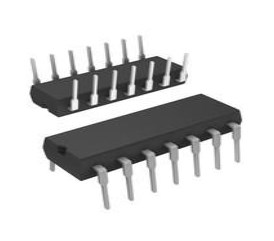
16 Termination 1.27mm 3/5V I/O Expander PCF8574 5V 16-SOIC (0.295, 7.50mm Width)
Unit Price: $1.069006
Ext Price: $1.07


16 Termination 1.27mm 3/5V I/O Expander PCF8574 5V 16-SOIC (0.295, 7.50mm Width)
PCF8574T is a remote 8-bit I/O expander for I2C-bus made by NXP Semiconductors. What do you want to know about it? PCF8574T datasheet? PCF8574T applications? PCF8574T Manufacturer? PCF8574T circuit? PCF8574T package? OK, Magi will tell them all for you.

PCF8574 I2C GPIO Expander Tutorial
PCF8574T Description
The PCF8574T IO Expansion Board is used as a remote 8-bit I/O expander for I2C-bus. Up to 8 PCF8574, T IO Expansion Board can be connected to the I2C-bus, providing up to 64 I/O ports.
The PCF8574T IO Expansion Board features allow the use of multi modules connected to the I2C bus at the same time by connecting the pin header and connector.
There is a small potentiometer on board, which can adjust the backlight of LCD1602 or LCD2004, and a jumper cap to control the switch of the LED light.
PCF8574T CAD Models
Symbol

Footprint

3D Models

PCF8574T Pinout and Configuration

| Pin No | Pin Name | Description |
| 1 | A0 | address input 0 |
| 2 | A1 | address input 1 |
| 3 | A2 | address input 2 |
| 4 | P0 | quasi-bidirectional I/O 0 |
| 5 | P1 | quasi-bidirectional I/O 1 |
| 6 | P2 | quasi-bidirectional I/O 2 |
| 7 | P3 | quasi-bidirectional I/O 3 |
| 8 | VSS | supply ground |
| 9 | P4 | quasi-bidirectional I/O 4 |
| 10 | P5 | quasi-bidirectional I/O 5 |
| 11 | P6 | quasi-bidirectional I/O 6 |
| 12 | P7 | quasi-bidirectional I/O 7 |
| 13 | INT | interrupt output (active LOW) |
| 14 | SCL | serial clock line |
| 15 | SDA | serial data line |
| 16 | VDD | supply voltage |
Specifications
- TypeParameter
- Factory Lead Time7 Weeks
- Mounting Type
The "Mounting Type" in electronic components refers to the method used to attach or connect a component to a circuit board or other substrate, such as through-hole, surface-mount, or panel mount.
Surface Mount - Package / Case
refers to the protective housing that encases an electronic component, providing mechanical support, electrical connections, and thermal management.
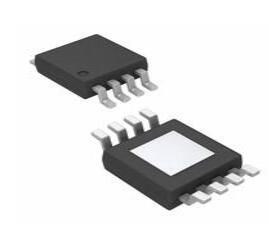
16-SOIC (0.295, 7.50mm Width) - Surface Mount
having leads that are designed to be soldered on the side of a circuit board that the body of the component is mounted on.
YES - Number of I/Os8
- Operating Temperature
The operating temperature is the range of ambient temperature within which a power supply, or any other electrical equipment, operate in. This ranges from a minimum operating temperature, to a peak or maximum operating temperature, outside which, the power supply may fail.
-40°C~85°C - Packaging
Semiconductor package is a carrier / shell used to contain and cover one or more semiconductor components or integrated circuits. The material of the shell can be metal, plastic, glass or ceramic.
Tube - Published1997
- JESD-609 Code
The "JESD-609 Code" in electronic components refers to a standardized marking code that indicates the lead-free solder composition and finish of electronic components for compliance with environmental regulations.
e4 - Part Status
Parts can have many statuses as they progress through the configuration, analysis, review, and approval stages.
Active - Moisture Sensitivity Level (MSL)
Moisture Sensitivity Level (MSL) is a standardized rating that indicates the susceptibility of electronic components, particularly semiconductors, to moisture-induced damage during storage and the soldering process, defining the allowable exposure time to ambient conditions before they require special handling or baking to prevent failures
2 (1 Year) - Number of Terminations16
- Terminal Finish
Terminal Finish refers to the surface treatment applied to the terminals or leads of electronic components to enhance their performance and longevity. It can improve solderability, corrosion resistance, and overall reliability of the connection in electronic assemblies. Common finishes include nickel, gold, and tin, each possessing distinct properties suitable for various applications. The choice of terminal finish can significantly impact the durability and effectiveness of electronic devices.
Nickel/Palladium/Gold (Ni/Pd/Au) - Voltage - Supply
Voltage - Supply refers to the range of voltage levels that an electronic component or circuit is designed to operate with. It indicates the minimum and maximum supply voltage that can be applied for the device to function properly. Providing supply voltages outside this range can lead to malfunction, damage, or reduced performance. This parameter is critical for ensuring compatibility between different components in a circuit.
2.5V~6V - Terminal Position
In electronic components, the term "Terminal Position" refers to the physical location of the connection points on the component where external electrical connections can be made. These connection points, known as terminals, are typically used to attach wires, leads, or other components to the main body of the electronic component. The terminal position is important for ensuring proper connectivity and functionality of the component within a circuit. It is often specified in technical datasheets or component specifications to help designers and engineers understand how to properly integrate the component into their circuit designs.
DUAL - Terminal Form
Occurring at or forming the end of a series, succession, or the like; closing; concluding.
GULL WING - Peak Reflow Temperature (Cel)
Peak Reflow Temperature (Cel) is a parameter that specifies the maximum temperature at which an electronic component can be exposed during the reflow soldering process. Reflow soldering is a common method used to attach electronic components to a circuit board. The Peak Reflow Temperature is crucial because it ensures that the component is not damaged or degraded during the soldering process. Exceeding the specified Peak Reflow Temperature can lead to issues such as component failure, reduced performance, or even permanent damage to the component. It is important for manufacturers and assemblers to adhere to the recommended Peak Reflow Temperature to ensure the reliability and functionality of the electronic components.
260 - Supply Voltage
Supply voltage refers to the electrical potential difference provided to an electronic component or circuit. It is crucial for the proper operation of devices, as it powers their functions and determines performance characteristics. The supply voltage must be within specified limits to ensure reliability and prevent damage to components. Different electronic devices have specific supply voltage requirements, which can vary widely depending on their design and intended application.
5V - Terminal Pitch
The center distance from one pole to the next.
1.27mm - Time@Peak Reflow Temperature-Max (s)
Time@Peak Reflow Temperature-Max (s) refers to the maximum duration that an electronic component can be exposed to the peak reflow temperature during the soldering process, which is crucial for ensuring reliable solder joint formation without damaging the component.
NOT SPECIFIED - Base Part Number
The "Base Part Number" (BPN) in electronic components serves a similar purpose to the "Base Product Number." It refers to the primary identifier for a component that captures the essential characteristics shared by a group of similar components. The BPN provides a fundamental way to reference a family or series of components without specifying all the variations and specific details.
PCF8574 - Pin Count
a count of all of the component leads (or pins)
16 - JESD-30 Code
JESD-30 Code refers to a standardized descriptive designation system established by JEDEC for semiconductor-device packages. This system provides a systematic method for generating designators that convey essential information about the package's physical characteristics, such as size and shape, which aids in component identification and selection. By using JESD-30 codes, manufacturers and engineers can ensure consistency and clarity in the specification of semiconductor packages across various applications and industries.
R-PDSO-G16 - Qualification Status
An indicator of formal certification of qualifications.
Not Qualified - Output Type
The "Output Type" parameter in electronic components refers to the type of signal or data that is produced by the component as an output. This parameter specifies the nature of the output signal, such as analog or digital, and can also include details about the voltage levels, current levels, frequency, and other characteristics of the output signal. Understanding the output type of a component is crucial for ensuring compatibility with other components in a circuit or system, as well as for determining how the output signal can be utilized or processed further. In summary, the output type parameter provides essential information about the nature of the signal that is generated by the electronic component as its output.
Push-Pull - Power Supplies
an electronic circuit that converts the voltage of an alternating current (AC) into a direct current (DC) voltage.?
3/5V - Interface
In electronic components, the term "Interface" refers to the point at which two different systems, devices, or components connect and interact with each other. It can involve physical connections such as ports, connectors, or cables, as well as communication protocols and standards that facilitate the exchange of data or signals between the connected entities. The interface serves as a bridge that enables seamless communication and interoperability between different parts of a system or between different systems altogether. Designing a reliable and efficient interface is crucial in ensuring proper functionality and performance of electronic components and systems.
I2C - Number of Ports
A port is identified for each transport protocol and address combination by a 16-bit unsigned number,.
1 - Number of Bits8
- Clock Frequency
Clock frequency, also known as clock speed, refers to the rate at which a processor or electronic component can execute instructions. It is measured in hertz (Hz) and represents the number of cycles per second that the component can perform. A higher clock frequency typically indicates a faster processing speed and better performance. However, it is important to note that other factors such as architecture, efficiency, and workload also play a significant role in determining the overall performance of a component. In summary, clock frequency is a crucial parameter that influences the speed and efficiency of electronic components in processing data and executing tasks.
100kHz - Supply Current-Max
Supply Current-Max refers to the maximum amount of current that an electronic component or circuit can draw from its power supply under specified operating conditions. It is a critical parameter that determines the power consumption and thermal performance of the device. Exceeding this limit can lead to overheating, potential damage, or failure of the component. Knowing the Supply Current-Max helps in designing circuits that ensure proper operation and reliability.
0.1mA - External Data Bus Width
The External Data Bus Width refers to the number of bits that can be transmitted simultaneously between a microprocessor and external components, such as memory or peripherals. It determines the amount of data that can be transferred in a single clock cycle. A wider data bus allows for faster data transfer rates and can improve overall system performance. Common data bus widths include 8-bit, 16-bit, 32-bit, and 64-bit, with larger widths generally offering higher throughput but requiring more complex circuitry. The External Data Bus Width is an important parameter to consider when designing or evaluating electronic components to ensure compatibility and optimal performance.
1 - Interrupt Output
In electronic components, "Interrupt Output" refers to a feature that allows a device to signal the occurrence of a specific event or condition that requires immediate attention from the system or user. When the specified event occurs, the interrupt output generates a signal to pause the normal operation of the device and divert the attention to handle the urgent task. This feature is commonly used in microcontrollers, processors, and other integrated circuits to efficiently manage tasks and prioritize critical operations. By utilizing interrupt outputs, electronic systems can respond promptly to important events, improve overall performance, and enhance real-time responsiveness.
Yes - Current - Output Source/Sink
The parameter "Current - Output Source/Sink" in electronic components refers to the maximum amount of current that the component can either source (provide) or sink (absorb) at its output pin. This parameter is crucial in determining the capability of the component to drive external loads such as other components or devices. The source current indicates the maximum current that the component can supply to the load, while the sink current indicates the maximum current that the component can draw from the load. Understanding this parameter is essential for designing circuits that require specific current-handling capabilities to ensure proper functionality and reliability.
300μA 25mA - Features
In the context of electronic components, the term "Features" typically refers to the specific characteristics or functionalities that a particular component offers. These features can vary depending on the type of component and its intended use. For example, a microcontroller may have features such as built-in memory, analog-to-digital converters, and communication interfaces like UART or SPI.When evaluating electronic components, understanding their features is crucial in determining whether they meet the requirements of a particular project or application. Engineers and designers often look at features such as operating voltage, speed, power consumption, and communication protocols to ensure compatibility and optimal performance.In summary, the "Features" parameter in electronic components describes the unique attributes and capabilities that differentiate one component from another, helping users make informed decisions when selecting components for their electronic designs.
POR - Length10.3mm
- Height Seated (Max)
Height Seated (Max) is a parameter in electronic components that refers to the maximum allowable height of the component when it is properly seated or installed on a circuit board or within an enclosure. This specification is crucial for ensuring proper fit and alignment within the overall system design. Exceeding the maximum seated height can lead to mechanical interference, electrical shorts, or other issues that may impact the performance and reliability of the electronic device. Manufacturers provide this information to help designers and engineers select components that will fit within the designated space and function correctly in the intended application.
2.65mm - Width7.5mm
- RoHS Status
RoHS means “Restriction of Certain Hazardous Substances” in the “Hazardous Substances Directive” in electrical and electronic equipment.
ROHS3 Compliant
PCF8574T Features
2C-bus to the parallel port expander
100 kHz I2C-bus interface (Standard-mode I2C-bus)
Operating supply voltage 2.5 V to 6 V with non-overvoltage tolerant I/O held to VDD with 100 mA current source
8-bit remote I/O pins that default to inputs at power-up
Latched outputs directly drive LEDs
Total package sink capability of 80 mA
The active LOW open-drain interrupt output
Eight programmable slave addresses using three address pins
Low standby current (2.5 mA typical)
-40 ℃ to +85 ℃ operation
ESD protection exceeds 2000 V HBM per JESD22-A114 and 1000 V CDM per JESD22-C101
Latch-up testing is done to JEDEC Standard JESD78 which exceeds 100 mA
Packages offered: DIP16, SO16, SSOP20
PCF8574T Alternatives
PCF8574T Circuit
The example circuit diagram is shown in the image below.

The main component of the I2C LCD display is the PCF8574 I/O expander, with only two pins SDA and SCL we get a maximum of 8 pins from P0 to P7. PCF8574A also can be used but it has a different address.
All LCD data pins are connected to the PCF8574 where: RS, RW, E, D4, D5, D6, and D7 are connected to P0, P1, P2, P4, P5, P6, and P7 respectively.
PCF8574 I/O expander SDA and SCL pins are connected to Arduino pins A4 and A5 respectively (Arduino SDA and SCL pins).
PCF8574 I/O expander A0, A1, and A2 pins are the address pins that decide the I2C address of the chip. In this example, each pin is connected to +5V through a 10k ohm resistor (the 10k resistor is optional, each pin can be connected directly to +5V).
The I2C address of the PCF8574 is: 0x20 | A2 A1 A0 ( | means OR)
In our circuit A2, A1 and A0 are connected to +5V (through 10k resistors) which means the I2C address is equal to 0x20 | 7 = 0x27
If the PCF8574A is used instead of the PCF8574 the I2C address is: 0x38 | 7 = 0x3F.
PCF8574T Manufacturer
NXP Semiconductors N.V. (NXP) is a Dutch semiconductor designer and manufacturer with headquarters in Eindhoven, Netherlands. The company employs approximately 29,000 people in more than 30 countries. NXP reported revenue of $11.06 billion in 2021.
Originally spun off from Philips in 2006, NXP completed its initial public offering, on August 6, 2010, with shares trading on NASDAQ under the ticker symbol NXPI. On December 23, 2013, NXP Semiconductors was added to the NASDAQ 100. On March 2, 2015, it was announced that NXP would merge with Freescale Semiconductor. The merger was closed on December 7, 2015. On October 27, 2016, it was announced that Qualcomm would try to buy NXP. Because the Chinese merger authority did not approve the acquisition before the deadline set by Qualcomm, the attempt was effectively canceled on July 26, 2018.
PCF8574T Block Diagram

PCF8574T Package


SO-16
Trend Analysis
Datasheet PDF
- Datasheets :
- Environmental Information :
Parts with Similar Specs
- ImagePart NumberManufacturerPackage / CaseInterfaceSupply VoltageTechnologyTerminal PitchPin CountWidthNumber of PortsView Compare
![PCF8574T/3,512]()
PCF8574T/3,512
16-SOIC (0.295, 7.50mm Width)
I2C
5 V
CMOS
1.27 mm
16
7.5 mm
1
![PCF8574AT/3,518]()
16-SOIC (0.295, 7.50mm Width)
I2C
5 V
CMOS
1.27 mm
16
7.5 mm
1
![PCF8574AT/3,512]()
16-SOIC (0.295, 7.50mm Width)
I2C, SMBus
3 V
CMOS
1.27 mm
16
7.5 mm
1
![PCF8574ADW]()
16-SOIC (0.295, 7.50mm Width)
I2C
5 V
CMOS
1.27 mm
16
7.5 mm
1
![PCA9554AD,112]()
16-SOIC (0.295, 7.50mm Width)
I2C
5 V
CMOS
1.27 mm
16
7.5 mm
1


What is I2C converter?
I2C LCD adapter is a device containing a micro-controller PCF8574 chip.
What is I2c module?
I2C Module has an inbuilt PCF8574 I2C chip that converts I2C serial data to parallel data for the LCD display.
What is I2C used for?
The I2C protocol is used to establish communication between two or more ICs (Integrated Circuits), hence why it's known as Inter-Integrated Circuit (I2C) communication.
How do I program PCF8574?
After connecting the I2C Module to LCD, connect the GND and VCC pins of the PCF8574 Module to the GND and 5V pins of Arduino. Finally, the SDA and SCL Pins. Connect them to pins A4 and A5 pins of Arduino UNO respectively.
What is pcf8574t?
The PCF8574/74A provides general-purpose remote I/O expansion via the two-wire bidirectional I2C-bus (serial clock (SCL), serial data (SDA)). The devices consist of eight quasi-bidirectional ports, a 100 kHz I2C-bus interface, three hardware address inputs, and interrupt output operating between 2.5 V and 6 V.
 TL074CN: 3MHz,Solder temperature, Pinout and Datasheet
21 February 20223828
 STM32F407ZET6 Microcontroller: Features, Applications and Datasheet
24 November 20236508
 STM8L151K6U3 Microcontroller: Technical Overview and Applications
29 February 2024135
 SST25VF040B 4-Mbit SPI Serial Flash: Pinout, Equivalent and Datasheet
31 March 20221202
 AD4005 16-Bit 1 MSPS SAR ADC: Eliminating High-Speed Drivers with Easy Drive Technology
06 May 2026147
 STM32U575VGT6 Price Trends 2025: Best Buying Strategies & Vendor Comparison
05 July 2025378
 DS620 Temperature Sensor: Pinout, Application, Alternatives, Datasheet
28 July 20211409
 BC637 NPN Transistor: Circuit, Pinout, and Datasheet
21 April 20222820
 Semiconductor Inspection System Market Expected to Reach US$ 8,380.01 Million By 2030
15 September 20233727
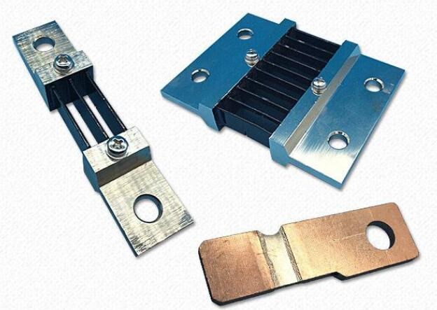 What are Shunts?
07 December 20207743
 What is a Fiber Optic Sensor?
31 October 202510449
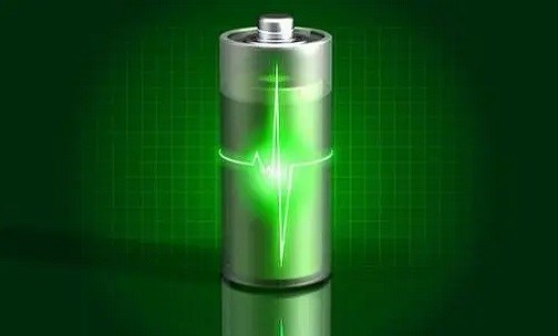 4680 Battery - Upgrade of Battery Technology
17 December 20216775
 Stanford Engineer Sheds Light on Semiconductors: Their Importance, Challenges, and Future
22 September 20231941
 Advantages of Single-Phase Liquid Immersion Cooling Technology
13 November 20232822
 A Combo for Innovation: Open Source and Crowdfunding
15 November 20195381
 Revolutionizing Semiconductor Manufacturing with New Plasma Power Technologies
23 September 20232333
NXP USA Inc.
In Stock: 1
Minimum: 1 Multiples: 1
Qty
Unit Price
Ext Price
1
$1.069006
$1.07
10
$1.008496
$10.08
100
$0.951412
$95.14
500
$0.897558
$448.78
1000
$0.846753
$846.75
Not the price you want? Send RFQ Now and we'll contact you ASAP.
Inquire for More Quantity
![PCA9534PW,118]() PCA9534PW,118
PCA9534PW,118NXP USA Inc.
![PCAL6524HEAZ]() PCAL6524HEAZ
PCAL6524HEAZNXP USA Inc.
![PCA9535PW,118]() PCA9535PW,118
PCA9535PW,118NXP USA Inc.
![PCF8574T/3,518]() PCF8574T/3,518
PCF8574T/3,518NXP USA Inc.
![PCAL6408ABSHP]() PCAL6408ABSHP
PCAL6408ABSHPNXP USA Inc.
![PCA9555BS,118]() PCA9555BS,118
PCA9555BS,118NXP USA Inc.
![PCA9554PW,118]() PCA9554PW,118
PCA9554PW,118NXP USA Inc.
![PCA9539BS,118]() PCA9539BS,118
PCA9539BS,118NXP USA Inc.
![PCA9698BS,118]() PCA9698BS,118
PCA9698BS,118NXP USA Inc.
![PCA9539APW,118]() PCA9539APW,118
PCA9539APW,118NXP USA Inc.


