

 Product
 Brand
Brand Articles
 Tools
Tools
TPS22919DCKR Load Switch: Features, Pinout, and Datasheet


N-Channel 0.65mm PMIC TPS22919 6-TSSOP, SC-88, SOT-363
The TPS22919 is a 6-pin SOT-23 device with a 5.5-V, 1.5-A load switch. This article mainly introduces Features, Pinout, Datasheet and other detailed information about Texas Instruments TPS22919DCKR.

What is a load switch
TPS22919DCKR Description
The TPS22919DCKR is a 6-pin SOT-23 device with a 5.5-V, 1.5-A load switch. The device uses a low resistance N-channel MOSFET to reduce voltage drop for low voltage and high current rails, lowering the drop-out voltage across the device.
A digital input capable of directly connecting with low-voltage control signals controls the switch ON state. A Smart Pull Down is utilized to keep the ON pin from floating until the system sequence is complete when power is initially delivered. The Smart Pull Down will be disconnected once the pin is intentionally driven high (>VIH) to prevent unnecessary power loss.
The TPS22919DCKR load switch is also self-protected, which means it will protect itself in the event of a short circuit on the device's output. It also supports thermal shutdown to prevent overheating damage.
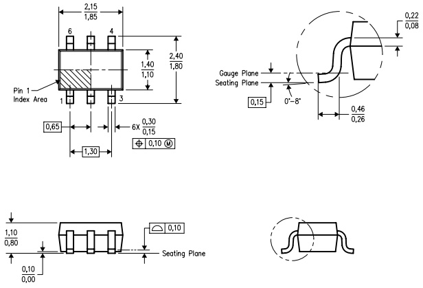
TPS22919DCKR is offered in a standard SC-70 package with a junction temperature range of –40°C to 125°C for operation.
TPS22919DCKR Pinout
The following figure is TPS22919DCKR Pinout.
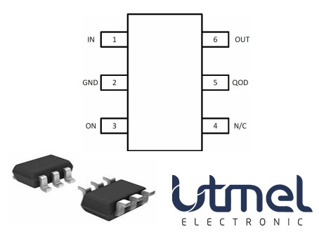
Pinout
| Pin Number | Pin Name | Description |
| 1 | IN | Switch input. |
| 2 | GND | Device ground. |
| 3 | ON | Active high switch control input. Do not leave floating. |
| 4 | NC | No connect pin, leave floating. |
| 5 | QOD | Quick Output Discharge pin. This functionality can be enabled in one of three ways. • Placing an external resistor between VOUT and QOD • Tying QOD directly to VOUT and using the internal resistor value (RPD) • Disabling QOD by leaving pin floating |
| 6 | VOUT | Switch output. |
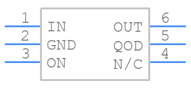
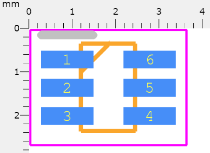
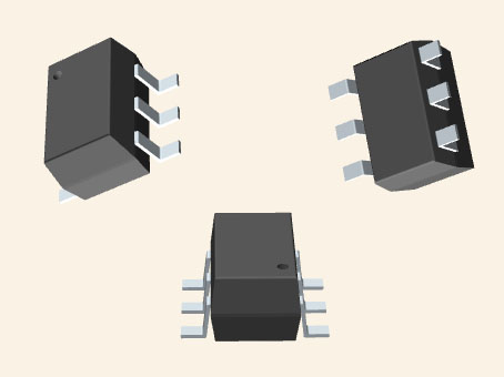
TPS22919DCKR CAD Model
TPS22919DCKR Features
• Input operating voltage range (VIN): 1.6 V to 5.5 V
• Maximum continuous current (IMAX): 1.5 A • On-Resistance (RON):
– 5-V VIN: 89 mΩ (typical)
– 3.6-V VIN: 90 mΩ (typical)
– 1.8-V VIN: 105 mΩ (typical)
• Output short protection (ISC): 3 A (typical)
• Low power consumption:
– ON state (IQ): 8 µA (typical)
– OFF state (ISD): 2 nA (typical)
• Smart ON pin pull down (RPD):
– ON ≥ VIH (ION): 100 nA (maximum)
– ON ≤ VIL (RPD): 530 kΩ (typical)
• Slow Turn ON timing to limit inrush current (tON):
– 5.0 V Turn ON time (tON): 1.95 ms at 3.2 mV/μs
– 3.6 V Turn ON time (tON): 1.75 ms at 2.7 mV/μs
– 1.8 V Turn ON time (tON): 1.5 ms at 1.8 mV/μs
• Adjustable output discharge and fall time:
– Internal QOD resistance = 24 Ω (typical)
Specifications
- TypeParameter
- Factory Lead Time6 Weeks
- Mounting Type
The "Mounting Type" in electronic components refers to the method used to attach or connect a component to a circuit board or other substrate, such as through-hole, surface-mount, or panel mount.
Surface Mount - Package / Case
refers to the protective housing that encases an electronic component, providing mechanical support, electrical connections, and thermal management.
6-TSSOP, SC-88, SOT-363 - Surface Mount
having leads that are designed to be soldered on the side of a circuit board that the body of the component is mounted on.
YES - Operating Temperature
The operating temperature is the range of ambient temperature within which a power supply, or any other electrical equipment, operate in. This ranges from a minimum operating temperature, to a peak or maximum operating temperature, outside which, the power supply may fail.
-40°C~125°C TA - Packaging
Semiconductor package is a carrier / shell used to contain and cover one or more semiconductor components or integrated circuits. The material of the shell can be metal, plastic, glass or ceramic.
Tape & Reel (TR) - JESD-609 Code
The "JESD-609 Code" in electronic components refers to a standardized marking code that indicates the lead-free solder composition and finish of electronic components for compliance with environmental regulations.
e3 - Pbfree Code
The "Pbfree Code" parameter in electronic components refers to the code or marking used to indicate that the component is lead-free. Lead (Pb) is a toxic substance that has been widely used in electronic components for many years, but due to environmental concerns, there has been a shift towards lead-free alternatives. The Pbfree Code helps manufacturers and users easily identify components that do not contain lead, ensuring compliance with regulations and promoting environmentally friendly practices. It is important to pay attention to the Pbfree Code when selecting electronic components to ensure they meet the necessary requirements for lead-free applications.
yes - Part Status
Parts can have many statuses as they progress through the configuration, analysis, review, and approval stages.
Active - Moisture Sensitivity Level (MSL)
Moisture Sensitivity Level (MSL) is a standardized rating that indicates the susceptibility of electronic components, particularly semiconductors, to moisture-induced damage during storage and the soldering process, defining the allowable exposure time to ambient conditions before they require special handling or baking to prevent failures
1 (Unlimited) - Number of Terminations6
- Terminal Finish
Terminal Finish refers to the surface treatment applied to the terminals or leads of electronic components to enhance their performance and longevity. It can improve solderability, corrosion resistance, and overall reliability of the connection in electronic assemblies. Common finishes include nickel, gold, and tin, each possessing distinct properties suitable for various applications. The choice of terminal finish can significantly impact the durability and effectiveness of electronic devices.
Matte Tin (Sn) - Voltage - Supply
Voltage - Supply refers to the range of voltage levels that an electronic component or circuit is designed to operate with. It indicates the minimum and maximum supply voltage that can be applied for the device to function properly. Providing supply voltages outside this range can lead to malfunction, damage, or reduced performance. This parameter is critical for ensuring compatibility between different components in a circuit.
Not Required - Terminal Position
In electronic components, the term "Terminal Position" refers to the physical location of the connection points on the component where external electrical connections can be made. These connection points, known as terminals, are typically used to attach wires, leads, or other components to the main body of the electronic component. The terminal position is important for ensuring proper connectivity and functionality of the component within a circuit. It is often specified in technical datasheets or component specifications to help designers and engineers understand how to properly integrate the component into their circuit designs.
DUAL - Terminal Form
Occurring at or forming the end of a series, succession, or the like; closing; concluding.
GULL WING - Number of Functions1
- Terminal Pitch
The center distance from one pole to the next.
0.65mm - Base Part Number
The "Base Part Number" (BPN) in electronic components serves a similar purpose to the "Base Product Number." It refers to the primary identifier for a component that captures the essential characteristics shared by a group of similar components. The BPN provides a fundamental way to reference a family or series of components without specifying all the variations and specific details.
TPS22919 - JESD-30 Code
JESD-30 Code refers to a standardized descriptive designation system established by JEDEC for semiconductor-device packages. This system provides a systematic method for generating designators that convey essential information about the package's physical characteristics, such as size and shape, which aids in component identification and selection. By using JESD-30 codes, manufacturers and engineers can ensure consistency and clarity in the specification of semiconductor packages across various applications and industries.
R-PDSO-G6 - Number of Outputs1
- Output Type
The "Output Type" parameter in electronic components refers to the type of signal or data that is produced by the component as an output. This parameter specifies the nature of the output signal, such as analog or digital, and can also include details about the voltage levels, current levels, frequency, and other characteristics of the output signal. Understanding the output type of a component is crucial for ensuring compatibility with other components in a circuit or system, as well as for determining how the output signal can be utilized or processed further. In summary, the output type parameter provides essential information about the nature of the signal that is generated by the electronic component as its output.
N-Channel - Interface
In electronic components, the term "Interface" refers to the point at which two different systems, devices, or components connect and interact with each other. It can involve physical connections such as ports, connectors, or cables, as well as communication protocols and standards that facilitate the exchange of data or signals between the connected entities. The interface serves as a bridge that enables seamless communication and interoperability between different parts of a system or between different systems altogether. Designing a reliable and efficient interface is crucial in ensuring proper functionality and performance of electronic components and systems.
On/Off - Output Configuration
Output Configuration in electronic components refers to the arrangement or setup of the output pins or terminals of a device. It defines how the output signals are structured and how they interact with external circuits or devices. The output configuration can determine the functionality and compatibility of the component in a circuit design. Common types of output configurations include single-ended, differential, open-drain, and push-pull configurations, each serving different purposes and applications in electronic systems. Understanding the output configuration of a component is crucial for proper integration and operation within a circuit.
High Side - Input Type
Input type in electronic components refers to the classification of the signal or data that a component can accept for processing or conversion. It indicates whether the input is analog, digital, or a specific format such as TTL or CMOS. Understanding input type is crucial for ensuring compatibility between different electronic devices and circuits, as it determines how signals are interpreted and interacted with.
Non-Inverting - Switch Type
Based on their characteristics, there are basically three types of switches: Linear switches, tactile switches and clicky switches.
General Purpose - Ratio - Input:Output
The parameter "Ratio - Input:Output" in electronic components refers to the relationship between the input and output quantities of a device or system. It is a measure of how the input signal or energy is transformed or converted into the output signal or energy. This ratio is often expressed as a numerical value or percentage, indicating the efficiency or effectiveness of the component in converting the input to the desired output. A higher ratio typically signifies better performance or higher efficiency, while a lower ratio may indicate losses or inefficiencies in the conversion process. Understanding and optimizing the input-output ratio is crucial in designing and evaluating electronic components for various applications.
1:1 - Voltage - Load
Voltage - Load refers to the voltage across a load component in an electronic circuit when it is connected and operational. It represents the electrical potential difference that drives current through the load, which can be a resistor, motor, or other devices that consume electrical power. The voltage - load relationship is crucial for determining how much power the load will utilize and how it will affect the overall circuit performance. Properly managing voltage - load is essential for ensuring devices operate efficiently and safely within their specified limits.
1.6V~5.5V - Fault Protection
Protection against electric shock under. single fault conditions.
Short Circuit - Output Peak Current Limit-Nom
Output Peak Current Limit-Nom is a parameter in electronic components that specifies the maximum current that can be delivered by the output under normal operating conditions. This limit is typically set to protect the component from damage due to excessive current flow. It ensures that the component operates within its safe operating limits and prevents overheating or other potential issues. Designers and engineers use this parameter to ensure proper functioning and reliability of the electronic system in which the component is used.
3A - Rds On (Typ)
The parameter "Rds On (Typ)" in electronic components refers to the typical on-state resistance of a MOSFET (Metal-Oxide-Semiconductor Field-Effect Transistor) when it is fully conducting. This parameter indicates the resistance encountered by the current flowing through the MOSFET when it is in the on-state, which affects the power dissipation and efficiency of the component. A lower Rds On value indicates better conduction and lower power loss in the MOSFET. Designers often consider this parameter when selecting components for applications where minimizing power loss and maximizing efficiency are critical factors.
89m Ω - Built-in Protections
Built-in protections in electronic components refer to the safety features and mechanisms that are integrated into the component to prevent damage or malfunction in various situations. These protections are designed to safeguard the component from overvoltage, overcurrent, overheating, short circuits, and other potential hazards that could occur during operation. By having built-in protections, electronic components can operate more reliably and safely, extending their lifespan and reducing the risk of failure. These protections are essential for ensuring the overall performance and longevity of electronic devices and systems.
TRANSIENT; OVER CURRENT; THERMAL - Output Current Flow Direction
Output Current Flow Direction refers to the orientation of current flowing out of a component or circuit. It indicates whether the current is being sourced from the component or sent to another component in the circuit. This parameter is crucial for understanding how electronic components interact within a circuit and ensures correct connectivity and functionality in circuit design. The direction can affect the operation and performance of the overall system.
SINK - Features
In the context of electronic components, the term "Features" typically refers to the specific characteristics or functionalities that a particular component offers. These features can vary depending on the type of component and its intended use. For example, a microcontroller may have features such as built-in memory, analog-to-digital converters, and communication interfaces like UART or SPI.When evaluating electronic components, understanding their features is crucial in determining whether they meet the requirements of a particular project or application. Engineers and designers often look at features such as operating voltage, speed, power consumption, and communication protocols to ensure compatibility and optimal performance.In summary, the "Features" parameter in electronic components describes the unique attributes and capabilities that differentiate one component from another, helping users make informed decisions when selecting components for their electronic designs.
Load Discharge, Slew Rate Controlled - Length2mm
- RoHS Status
RoHS means “Restriction of Certain Hazardous Substances” in the “Hazardous Substances Directive” in electrical and electronic equipment.
ROHS3 Compliant
TPS22919DCKR Functional Block Diagram
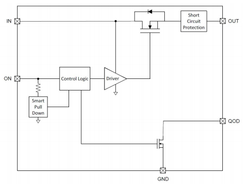
TPS22919DCKR Simplified Schematic
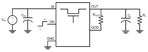
TPS22919DCKR Test Circuit
The TPS22919DCKR Test Circuit is shown as follows.
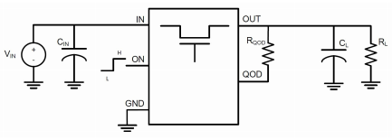
Test Circuit
(1) The control signal's rise and fall times are 100 nanoseconds.
(2) The time constant at the load affects the turn-off and fall times. When the switch is deactivated on the TPS22919 devices, the internal pull-down resistance QOD is enabled. (RQOD + RPD,QOD || RL) *CL is the time constant.
TPS22919DCKR Layout
All traces must be as brief as possible for optimal performance. In order to reduce the impacts of parasitic trace inductances on normal operation, the input and output capacitors must be located close to the device. The parasitic electrical effects are reduced by using large traces for VIN, VOUT, and GND.
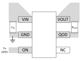
Layout
TPS22919DCKR Applications
• Personal electronics
• Set-top box
• HDTV
• Multi function printer
TPS22919DCKR Package
TPS22919DCKR Manufacturer
Texas Instruments (TI), a multinational semiconductor business with operations in 35 countries, is first and foremost a reflection of its employees. We are problem-solvers cooperating to transform the world via technology, from the TIer who introduced the first functional integrated circuit in 1958 to the more than 30,000 TIers throughout the world today who develop, build, and distribute analog and embedded processor chips.
Trend Analysis
What is the TPS22919DCKR?
5.5 V, 1.5 A, 90-mΩ Self-Protected Load Switch with Controlled Rise Time.
What does the TPS22919DCKR use to reduce voltage drop?
Low resistance N-channel MOSFET.
What does a digital input do to the TPS22919DCKR?
A digital input capable of directly connecting with low-voltage control signals controls the switch ON state.
What is used to keep the ON pin from floating until the system sequence is complete when power is initially delivered?
A Smart Pull Down.
What is the TPS22919DCKR load switch?
Self-protected.
What does the TPS22919DCKR support to prevent overheating damage?
Thermal shutdown.
What is the junction temperature range of the TPS22919DCKR?
–40°C to 125°C for operation.
 74LS107 Dual JK Flip-Flops: Flip-Flops Datasheet pdf, Pinout and Diagram
20 December 20216527
 Essential Tips for Using STM32H743ZIT6 in Projects
24 July 20252948
 SI5347 Clock Generator: Features, Pinout and Datasheet
18 April 20221159
 AD8397 310mA High-Output Op-Amp: Performance Analysis and PCB Layout Handbook
14 March 2026322
 AD7768 24-Bit 8-Channel ADC: High-Speed Simultaneous Sampling Deep Dive
10 March 20261014
 IRF9530 Power MOSFET: Pinout, Alternatives and Datasheet
08 September 20217877
 AD8221 Precision Instrumentation Amplifier: High CMRR Performance and Design Guide
25 February 2026697
 XC2331D 16/32-Bit Single-Chip Microcontroller: A Technical Overview
29 February 2024199
 What is An Optoisolator?
09 January 20218592
 How to Identify the Perfect Proximity Sensor for Your Application
19 July 20251845
 Humanoid Robot BOM Breakdown: Every Chip Inside a Physical AI Platform
28 July 2026917
 How are Integrated Circuits produced?
20 October 202526635
 What is a Wireless Network Adapter?
01 June 20216975
 What is a Reed Relay?
16 April 20219543
 The Introduction of Car Fuse
09 October 20216969
 What is an LTPO Display?
08 October 20219198
Texas Instruments
In Stock: 10000
United States
China
Canada
Japan
Russia
Germany
United Kingdom
Singapore
Italy
Hong Kong(China)
Taiwan(China)
France
Korea
Mexico
Netherlands
Malaysia
Austria
Spain
Switzerland
Poland
Thailand
Vietnam
India
United Arab Emirates
Afghanistan
Åland Islands
Albania
Algeria
American Samoa
Andorra
Angola
Anguilla
Antigua & Barbuda
Argentina
Armenia
Aruba
Australia
Azerbaijan
Bahamas
Bahrain
Bangladesh
Barbados
Belarus
Belgium
Belize
Benin
Bermuda
Bhutan
Bolivia
Bonaire, Sint Eustatius and Saba
Bosnia & Herzegovina
Botswana
Brazil
British Indian Ocean Territory
British Virgin Islands
Brunei
Bulgaria
Burkina Faso
Burundi
Cabo Verde
Cambodia
Cameroon
Cayman Islands
Central African Republic
Chad
Chile
Christmas Island
Cocos (Keeling) Islands
Colombia
Comoros
Congo
Congo (DRC)
Cook Islands
Costa Rica
Côte d’Ivoire
Croatia
Cuba
Curaçao
Cyprus
Czechia
Denmark
Djibouti
Dominica
Dominican Republic
Ecuador
Egypt
El Salvador
Equatorial Guinea
Eritrea
Estonia
Eswatini
Ethiopia
Falkland Islands
Faroe Islands
Fiji
Finland
French Guiana
French Polynesia
Gabon
Gambia
Georgia
Ghana
Gibraltar
Greece
Greenland
Grenada
Guadeloupe
Guam
Guatemala
Guernsey
Guinea
Guinea-Bissau
Guyana
Haiti
Honduras
Hungary
Iceland
Indonesia
Iran
Iraq
Ireland
Isle of Man
Israel
Jamaica
Jersey
Jordan
Kazakhstan
Kenya
Kiribati
Kosovo
Kuwait
Kyrgyzstan
Laos
Latvia
Lebanon
Lesotho
Liberia
Libya
Liechtenstein
Lithuania
Luxembourg
Macao(China)
Madagascar
Malawi
Maldives
Mali
Malta
Marshall Islands
Martinique
Mauritania
Mauritius
Mayotte
Micronesia
Moldova
Monaco
Mongolia
Montenegro
Montserrat
Morocco
Mozambique
Myanmar
Namibia
Nauru
Nepal
New Caledonia
New Zealand
Nicaragua
Niger
Nigeria
Niue
Norfolk Island
North Korea
North Macedonia
Northern Mariana Islands
Norway
Oman
Pakistan
Palau
Palestinian Authority
Panama
Papua New Guinea
Paraguay
Peru
Philippines
Pitcairn Islands
Portugal
Puerto Rico
Qatar
Réunion
Romania
Rwanda
Samoa
San Marino
São Tomé & Príncipe
Saudi Arabia
Senegal
Serbia
Seychelles
Sierra Leone
Sint Maarten
Slovakia
Slovenia
Solomon Islands
Somalia
South Africa
South Sudan
Sri Lanka
St Helena, Ascension, Tristan da Cunha
St. Barthélemy
St. Kitts & Nevis
St. Lucia
St. Martin
St. Pierre & Miquelon
St. Vincent & Grenadines
Sudan
Suriname
Svalbard & Jan Mayen
Sweden
Syria
Tajikistan
Tanzania
Timor-Leste
Togo
Tokelau
Tonga
Trinidad & Tobago
Tunisia
Turkey
Turkmenistan
Turks & Caicos Islands
Tuvalu
U.S. Outlying Islands
U.S. Virgin Islands
Uganda
Ukraine
Uruguay
Uzbekistan
Vanuatu
Vatican City
Venezuela
Wallis & Futuna
Yemen
Zambia
Zimbabwe
![TPS22913CYZVR]() TPS22913CYZVR
TPS22913CYZVRTexas Instruments
![TPS2052BDR]() TPS2052BDR
TPS2052BDRTexas Instruments
![TPS2051BDGNR]() TPS2051BDGNR
TPS2051BDGNRTexas Instruments
![TPS2044BD]() TPS2044BD
TPS2044BDTexas Instruments
![TPS2042BDR]() TPS2042BDR
TPS2042BDRTexas Instruments
![ULQ2003ADR]() ULQ2003ADR
ULQ2003ADRTexas Instruments
![TPS22945DCKR]() TPS22945DCKR
TPS22945DCKRTexas Instruments
![TPS2042BDGN]() TPS2042BDGN
TPS2042BDGNTexas Instruments
![TPS2557DRBT]() TPS2557DRBT
TPS2557DRBTTexas Instruments
![TPS2044BDR]() TPS2044BDR
TPS2044BDRTexas Instruments


