
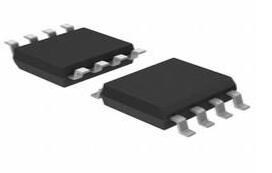
TPS61022RWUR Boost Converter, 0.5-V 7-VQFN and Switching Voltage Regulators

7 Terminals 0.5V TPS61022 DC DC Voltage Regulator SWITCHING REGULATOR 1 Outputs 600kHz 1MHz Tape & Reel (TR) 7-VFQFN
Unit Price: $0.238220
Ext Price: $0.24


7 Terminals 0.5V TPS61022 DC DC Voltage Regulator SWITCHING REGULATOR 1 Outputs 600kHz 1MHz Tape & Reel (TR) 7-VFQFN
TPS61022RWUR is an 8-A Boost Converter with 0.5-V Ultra-low Input Voltage. This article is going to explain guide details for you. Welcome your RFQ!

Boost Converters (DC-DC Step-Up)
- What is TPS61022RWUR?
- TPS61022RWUR Pinout
- TPS61022RWUR CAD Mode
- Specifications
- TPS61022RWUR Block Diagram
- TPS61022RWUR Features
- TPS61022RWUR Application
- TPS61022RWUR Application Circuit
- TPS61022RWUR Layout Example
- TPS61022RWUR Environmental and Export Classification
- TPS61022RWUR Package Dimensions
- TPS61022RWUR Manufacturer
What is TPS61022RWUR?
The TPS61022RWUR is an 8-A Boost Converter having a 0.5-V Input Voltage. The TPS61022RWUR is a power supply for portable equipment and IoT devices that are powered by batteries and supercapacitors of various types. Over the whole temperature range, the TPS61022RWUR has a minimum 6.5-A valley switch current limit. The TPS61022RWUR provides supercapacitor backup power applications with a wide input voltage range of 0.5 V to 5.5 V, even if the supercapacitor is deeply discharged.
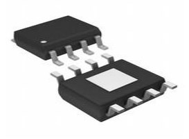
TPS61022RWUR Pinout

TPS61022RWUR Pinout
TPS61022RWUR CAD Mode

TPS61022RWUR Symbol

TPS61022RWUR Footprint

TPS61022RWUR 3D Model
Specifications
- TypeParameter
- Factory Lead Time16 Weeks
- Mounting Type
The "Mounting Type" in electronic components refers to the method used to attach or connect a component to a circuit board or other substrate, such as through-hole, surface-mount, or panel mount.
Surface Mount - Package / Case
refers to the protective housing that encases an electronic component, providing mechanical support, electrical connections, and thermal management.
7-VFQFN - Surface Mount
having leads that are designed to be soldered on the side of a circuit board that the body of the component is mounted on.
YES - Operating Temperature
The operating temperature is the range of ambient temperature within which a power supply, or any other electrical equipment, operate in. This ranges from a minimum operating temperature, to a peak or maximum operating temperature, outside which, the power supply may fail.
-40°C~125°C TJ - Packaging
Semiconductor package is a carrier / shell used to contain and cover one or more semiconductor components or integrated circuits. The material of the shell can be metal, plastic, glass or ceramic.
Tape & Reel (TR) - JESD-609 Code
The "JESD-609 Code" in electronic components refers to a standardized marking code that indicates the lead-free solder composition and finish of electronic components for compliance with environmental regulations.
e4 - Pbfree Code
The "Pbfree Code" parameter in electronic components refers to the code or marking used to indicate that the component is lead-free. Lead (Pb) is a toxic substance that has been widely used in electronic components for many years, but due to environmental concerns, there has been a shift towards lead-free alternatives. The Pbfree Code helps manufacturers and users easily identify components that do not contain lead, ensuring compliance with regulations and promoting environmentally friendly practices. It is important to pay attention to the Pbfree Code when selecting electronic components to ensure they meet the necessary requirements for lead-free applications.
yes - Part Status
Parts can have many statuses as they progress through the configuration, analysis, review, and approval stages.
Active - Moisture Sensitivity Level (MSL)
Moisture Sensitivity Level (MSL) is a standardized rating that indicates the susceptibility of electronic components, particularly semiconductors, to moisture-induced damage during storage and the soldering process, defining the allowable exposure time to ambient conditions before they require special handling or baking to prevent failures
2 (1 Year) - Number of Terminations7
- Terminal Finish
Terminal Finish refers to the surface treatment applied to the terminals or leads of electronic components to enhance their performance and longevity. It can improve solderability, corrosion resistance, and overall reliability of the connection in electronic assemblies. Common finishes include nickel, gold, and tin, each possessing distinct properties suitable for various applications. The choice of terminal finish can significantly impact the durability and effectiveness of electronic devices.
Nickel/Palladium/Gold (Ni/Pd/Au) - Terminal Position
In electronic components, the term "Terminal Position" refers to the physical location of the connection points on the component where external electrical connections can be made. These connection points, known as terminals, are typically used to attach wires, leads, or other components to the main body of the electronic component. The terminal position is important for ensuring proper connectivity and functionality of the component within a circuit. It is often specified in technical datasheets or component specifications to help designers and engineers understand how to properly integrate the component into their circuit designs.
DUAL - Terminal Form
Occurring at or forming the end of a series, succession, or the like; closing; concluding.
NO LEAD - Base Part Number
The "Base Part Number" (BPN) in electronic components serves a similar purpose to the "Base Product Number." It refers to the primary identifier for a component that captures the essential characteristics shared by a group of similar components. The BPN provides a fundamental way to reference a family or series of components without specifying all the variations and specific details.
TPS61022 - JESD-30 Code
JESD-30 Code refers to a standardized descriptive designation system established by JEDEC for semiconductor-device packages. This system provides a systematic method for generating designators that convey essential information about the package's physical characteristics, such as size and shape, which aids in component identification and selection. By using JESD-30 codes, manufacturers and engineers can ensure consistency and clarity in the specification of semiconductor packages across various applications and industries.
S-PDSO-N7 - Function
The parameter "Function" in electronic components refers to the specific role or purpose that the component serves within an electronic circuit. It defines how the component interacts with other elements, influences the flow of electrical signals, and contributes to the overall behavior of the system. Functions can include amplification, signal processing, switching, filtering, and energy storage, among others. Understanding the function of each component is essential for designing effective and efficient electronic systems.
Step-Up - Number of Outputs1
- Voltage - Input (Max)
Voltage - Input (Max) is a parameter in electronic components that specifies the maximum voltage that can be safely applied to the input of the component without causing damage. This parameter is crucial for ensuring the proper functioning and longevity of the component. Exceeding the maximum input voltage can lead to electrical overstress, which may result in permanent damage or failure of the component. It is important to carefully adhere to the specified maximum input voltage to prevent any potential issues and maintain the reliability of the electronic system.
5.5V - Output Voltage
Output voltage is a crucial parameter in electronic components that refers to the voltage level produced by the component as a result of its operation. It represents the electrical potential difference between the output terminal of the component and a reference point, typically ground. The output voltage is a key factor in determining the performance and functionality of the component, as it dictates the level of voltage that will be delivered to the connected circuit or load. It is often specified in datasheets and technical specifications to ensure compatibility and proper functioning within a given system.
5V - Output Type
The "Output Type" parameter in electronic components refers to the type of signal or data that is produced by the component as an output. This parameter specifies the nature of the output signal, such as analog or digital, and can also include details about the voltage levels, current levels, frequency, and other characteristics of the output signal. Understanding the output type of a component is crucial for ensuring compatibility with other components in a circuit or system, as well as for determining how the output signal can be utilized or processed further. In summary, the output type parameter provides essential information about the nature of the signal that is generated by the electronic component as its output.
Adjustable - Voltage - Input (Min)
Voltage - Input (Min) refers to the minimum voltage level that an electronic component requires to operate correctly. It indicates the lowest voltage that can be applied to the component while still allowing it to function as intended. If the input voltage falls below this specified minimum, the component may not perform properly or may fail to operate altogether. This parameter is critical for ensuring reliable operation and longevity of the device in electronic circuits.
0.5V - Input Voltage-Nom
Input Voltage-Nom refers to the nominal or rated input voltage that an electronic component or device is designed to operate within. This parameter specifies the voltage level at which the component is expected to function optimally and safely. It is important to ensure that the actual input voltage supplied to the component does not exceed this nominal value to prevent damage or malfunction. Manufacturers provide this specification to guide users in selecting the appropriate power supply or input voltage source for the component. It is a critical parameter to consider when designing or using electronic circuits to ensure reliable performance and longevity of the component.
3.6V - Analog IC - Other Type
Analog IC - Other Type is a parameter used to categorize electronic components that are integrated circuits (ICs) designed for analog signal processing but do not fall into more specific subcategories such as amplifiers, comparators, or voltage regulators. These ICs may include specialized analog functions such as analog-to-digital converters (ADCs), digital-to-analog converters (DACs), voltage references, or signal conditioning circuits. They are typically used in various applications where precise analog signal processing is required, such as in audio equipment, instrumentation, communication systems, and industrial control systems. Manufacturers provide detailed specifications for these components to help engineers select the most suitable IC for their specific design requirements.
SWITCHING REGULATOR - Output Configuration
Output Configuration in electronic components refers to the arrangement or setup of the output pins or terminals of a device. It defines how the output signals are structured and how they interact with external circuits or devices. The output configuration can determine the functionality and compatibility of the component in a circuit design. Common types of output configurations include single-ended, differential, open-drain, and push-pull configurations, each serving different purposes and applications in electronic systems. Understanding the output configuration of a component is crucial for proper integration and operation within a circuit.
Positive - Voltage - Output (Min/Fixed)
Voltage - Output (Min/Fixed) refers to the minimum fixed output voltage level that an electronic component, such as a voltage regulator or power supply, is designed to provide under specified load conditions. This parameter ensures that the device consistently delivers a reliable voltage that meets the requirements of the connected circuits or components. It is critical for applications where stable and predictable voltage is necessary for proper operation.
2.2V - Topology
In the context of electronic components, "topology" refers to the arrangement or configuration of the components within a circuit or system. It defines how the components are connected to each other and how signals flow between them. The choice of topology can significantly impact the performance, efficiency, and functionality of the electronic system. Common topologies include series, parallel, star, mesh, and hybrid configurations, each with its own advantages and limitations. Designers carefully select the appropriate topology based on the specific requirements of the circuit to achieve the desired performance and functionality.
Boost - Control Mode
In electronic components, "Control Mode" refers to the method or mode of operation used to regulate or control the behavior of the component. This parameter determines how the component responds to input signals or commands to achieve the desired output. The control mode can vary depending on the specific component and its intended function, such as voltage regulation, current limiting, or frequency modulation. Understanding the control mode of an electronic component is crucial for proper integration and operation within a circuit or system.
CURRENT-MODE - Frequency - Switching
"Frequency - Switching" in electronic components refers to the rate at which a device, such as a transistor or switching regulator, turns on and off during operation. This parameter is crucial in determining the efficiency and performance of power converters, oscillators, and other circuits that rely on rapid switching. Higher switching frequencies typically allow for smaller component sizes but may require more advanced design considerations to manage heat and electromagnetic interference.
600kHz 1MHz - Control Technique
In electronic components, "Control Technique" refers to the method or approach used to regulate and manage the operation of the component. This parameter is crucial in determining how the component functions within a circuit or system. Different control techniques can include analog control, digital control, pulse-width modulation (PWM), and various feedback mechanisms. The choice of control technique can impact the performance, efficiency, and overall functionality of the electronic component. It is important to select the appropriate control technique based on the specific requirements and characteristics of the application in which the component will be used.
PULSE WIDTH MODULATION - Synchronous Rectifier
Synchronous rectification is a technique for improving the efficiency of rectification by replacing diodes with actively controlled switches, usually power MOSFETs or power bipolar junction transistors (BJT).
Yes - Length2mm
- Width2mm
- RoHS Status
RoHS means “Restriction of Certain Hazardous Substances” in the “Hazardous Substances Directive” in electrical and electronic equipment.
ROHS3 Compliant
TPS61022RWUR Block Diagram

TPS61022RWUR Block Diagram
TPS61022RWUR Features
Input voltage range: 0.5 V to 5.5 V
1.8-V minimum input voltage for start-up
Output voltage setting range: 2.2 V to 5.5 V
Two 12-mΩ (LS) / 18-mΩ (HS) MOSFETs
8-A valley switching current limit
94.7% efficiency at VIN = 3.6 V, VOUT = 5 V and IOUT = 3 A
1-MHz switching frequency when VIN > 1.5 V and 0.6-MHz switching frequency when VIN < 1 V
±2.5% reference voltage accuracy over –40°C to +125°C
Pin-selectable auto PFM operation mode or forced PWM operation mode at light load
Pass-through mode when VIN > VOUT
True disconnection between input and output during shutdown
Output overvoltage and thermal shutdown protection
Output short-circuit protection
2-mm × 2-mm VQFN 7-pin package
TPS61022RWUR Application
USB port
Supercap backup
GPRS power supply
TPS61022RWUR Application Circuit

TPS61022RWUR Application Circuit
TPS61022RWUR Layout Example

TPS61022RWUR Layout Example
TPS61022RWUR Environmental and Export Classification
| Attribute | Description |
| RoHS Status | ROHS3 Compliant |
| Moisture Sensitivity Level (MSL) | 2 (1 Year) |
| REACH Status | REACH Unaffected |
| ECCN | EAR99 |
| HTSUS | 8542.39.0001 |
TPS61022RWUR Package Dimensions

TPS61022RWUR Package Dimensions
TPS61022RWUR Manufacturer
Texas Instruments Incorporated (TI) is an American technology company headquartered in Dallas, Texas, that designs and manufactures semiconductors and various integrated circuits, which it sells to electronics designers and manufacturers globally. It is one of the top 10 semiconductor companies worldwide based on sales volume.
What are the TPS61022RWUR powered by?
Batteries and super capacitors
What is the minimum temperature range of the TPS61022RWUR?
6.5-A valley switch current limit
What is the TPS61022RWUR?
8-A Boost Converter
What is the operating temperature of TPS61022RWUR?
-40°C~125°C TJ
How many pins of TPS61022RWUR?
7 Pins
 LM2576 Voltage Regulator: Features, Speicifications and Applications
19 May 2021927
 IR2153 Half-Bridge Driver: Datasheet, Circuit and Equivalent
14 October 202114024
![A6K SWITCH ROTARY DIP HEX 25MA 24V[Video]: Datasheet, Features, and Output Codes](https://res.utmel.com/Images/Article/d6e80446-68b3-42fa-b1d8-10bbce9388eb.png) A6K SWITCH ROTARY DIP HEX 25MA 24V[Video]: Datasheet, Features, and Output Codes
A6K SWITCH ROTARY DIP HEX 25MA 24V[Video]: Datasheet, Features, and Output Codes31 March 2022925
 MGA-81563 Amplifier: Pinout, Equivalent and Datasheet
07 April 20222079
 Exploring the STM32F410CBT6 Microcontroller: Features, Specifications, and Applications
29 February 2024152
 MCP1702 250 mA Low Quiescent Current LDO Regulator: Circuit, Datasheet pdf and Equivalents
26 November 20212843
 LM318 OP-AMP: Datasheet, Pinout, Alternatives and Circuit
09 September 20216426
 ADP7118 Linear Regulator: Features, Pinout and Datasheet
14 December 20211078
 Apple M1 Ultra -- The Technology Behind the Chip Interconnection
12 March 20224896
 MIT Technology Review Officially Released 2022 Top 10 Breakthrough Technologies in the World
26 April 20225364
 Automatic Voltage Regulator: Ultimate Guide to Stable Power and Equipment Protection
06 May 20255902
 Does the Terminal Resistance of the CAN Bus Have to be 120Ω?
19 April 202234243
 Hybrid Sources Powered Electric Vehicles - Part 2
20 March 20232669
 The Key Role of Electronic Components in IoT Devices
01 September 20235026
 What are Proximity Sensors?
24 October 20257568
 Logic - Translators, Level Shifters: A Semiconductor Device on A Circuit
22 February 20231683
Texas Instruments
In Stock: 9249
Minimum: 1 Multiples: 1
Qty
Unit Price
Ext Price
1
$0.238220
$0.24
10
$0.224736
$2.25
100
$0.212015
$21.20
500
$0.200015
$100.01
1000
$0.188693
$188.69
Not the price you want? Send RFQ Now and we'll contact you ASAP.
Inquire for More Quantity
![LM2574HVMX-3.3]() LM2574HVMX-3.3
LM2574HVMX-3.3Texas Instruments
![LM25574MTX]() LM25574MTX
LM25574MTXTexas Instruments
![LM2577MX-ADJ]() LM2577MX-ADJ
LM2577MX-ADJTexas Instruments
![TLV62565DBVR]() TLV62565DBVR
TLV62565DBVRTexas Instruments
![LM25011MY/NOPB]() LM25011MY/NOPB
LM25011MY/NOPBTexas Instruments
![LM2575T-5.0/NOPB]() LM2575T-5.0/NOPB
LM2575T-5.0/NOPBTexas Instruments
![MC33063ADR]() MC33063ADR
MC33063ADRTexas Instruments
![LM2675MX-ADJ/NOPB]() LM2675MX-ADJ/NOPB
LM2675MX-ADJ/NOPBTexas Instruments
![LM2574N-5.0/NOPB]() LM2574N-5.0/NOPB
LM2574N-5.0/NOPBTexas Instruments
![LM2576SX-5.0/NOPB]() LM2576SX-5.0/NOPB
LM2576SX-5.0/NOPBTexas Instruments


