
 Product
 Brand
Brand Articles
 Tools
Tools
ADP7118 Linear Regulator: Features, Pinout and Datasheet

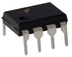
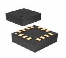
Enable, Soft Start Fixed ADP7118 PMIC 8 8-SOIC (0.154, 3.90mm Width) Exposed Pad
Unit Price: $2.273306
Ext Price: $2.27


Enable, Soft Start Fixed ADP7118 PMIC 8 8-SOIC (0.154, 3.90mm Width) Exposed Pad
The ADP7118 is a low quiescent current, LDO linear regulator that operates from 2.7 V to 20 V and provides up to 200 mA of output current. Drawing a low 180 μA of quiescent current (typical) at full load makes the ADP7118 ideal for portable equipment. Furthermore, Huge range of Semiconductors, Capacitors, Resistors and IcS in stock. Welcome RFQ.

Linear Regulator Operation Using a MOSFET
ADP7118 Pinout

Pinout
ADP7118 CAD Model

PCB Symbol

PCB Footprint

3D Model
ADP7118 Overview
The ADP7118 is a CMOS, low dropout (LDO) linear regulator that operates from 2.7 V to 20 V and provides up to 200 mA of output current. This high input voltage LDO is ideal for the regulation of high performance analog and mixed-signal circuits operating from 20 V down to 1.2 V rails. Using an advanced proprietary architecture, the device provides high power supply rejection, low noise, and achieves excellent line and load transient response with a small 2.2 μF ceramic output capacitor. The ADP7118 regulator output noise is 11 μV rms independent of the output voltage for the fixed options of 5 V or less. The ADP7118 is available in 16 fixed output voltage options. The following voltages are available from stock: 1.2 V (adjustable), 1.8 V, 2.5 V, 3.3 V, 4.5 V, and 5.0 V. Additional voltages available by special order are 1.5 V, 1.85 V, 2.0 V, 2.2 V, 2.75 V, 2.8 V, 2.85 V, 3.8 V, 4.2 V, and 4.6 V.
This article provides you with a basic overview of the ADP7118 Linear Regulator, including its pin descriptions, features and specifications, etc., to help you quickly understand what ADP7118 is.
ADP7118 Features
● Low noise: 11 μV rms independent of fixed output voltage PSRR of 88 dB at 10 kHz, 68 dB at 100 kHz, 50 dB at 1 MHz, VOUT ≤ 5 V, VIN = 7 V
● Input voltage range: 2.7 V to 20 V
● Maximum output current: 200 mA
● Initial accuracy: ±0.8%
● Accuracy over line, load, and temperature
◆ −1.2% to +1.5%, TJ = −40°C to +85°C
◆ ±1.8%, TJ = −40°C to +125°C
● Low dropout voltage: 200 mV (typical) at a 200 mA load, VOUT = 5 V
● User programmable soft start (LFCSP and SOIC only)
● Low quiescent current, IGND = 50 μA (typical) with no load
● Low shutdown current: 1.8 μA at VIN = 5 V, 3.0 μA at VIN = 20 V
● Stable with a small 2.2 μF ceramic output capacitor
● Fixed output voltage options: 1.8 V, 2.5 V, 3.3 V, 4.5 V, and 5.0 V, 16 standard voltages between 1.2 V and 5.0 V are available
● Adjustable output from 1.2 V to VIN – VDO, output can be adjusted above initial set point
● Precision enable
● 2 mm × 2 mm, 6-lead LFCSP, 8-Lead SOIC, 5-Lead TSOT
● AEC-Q100 qualified for automotive applications
ADP7118 Advantage
The ADP7118 is available in a 6-lead, 2 mm × 2 mm LFCSP making it not only a very compact solution, but it also provides excellent thermal performance for applications requiring up to 200 mA of output current in a small, low profile footprint. The ADP7118 is also available in a 5-lead TSOT and an 8-lead SOIC. The ADP7118 is available in 16 fixed output voltage options, ranging from 1.2 V to 5.0 V. The ADP7118 architecture allows any fixed output voltage to be set to a higher voltage with an external voltage divider.
The ADP7118 uses the EN pin to enable and disable the VOUT pin under normal operating conditions. When EN is high, VOUT turns on, and when EN is low, VOUT turns off. For automatic startup, EN can be tied to VIN. The ADP7118 is supported by the ADIsimPower™ design tool set. ADIsimPower is a collection of tools that produce complete power designs optimized for a specific design goal. The tools enable the user to generate a full schematic, bill of materials, and calculate performance in minutes. The ADP7118 is designed for operation with small, space-saving ceramic capacitors, but functions with general-purpose capacitors as long as care is taken with regard to the effective series resistance (ESR) value. The ADP7118 uses an internal soft start (SS pin open) to limit the inrush current when the output is enabled. The ADP7118 is protected against damage due to excessive power dissipation by current and thermal overload protection circuits. The ADP7118 is designed to current limit when the output load reaches 400 mA (typical). When the output load exceeds 400 mA, the output voltage is reduced to maintain a constant current limit.
Specifications
- TypeParameter
- Lifecycle Status
Lifecycle Status refers to the current stage of an electronic component in its product life cycle, indicating whether it is active, obsolete, or transitioning between these states. An active status means the component is in production and available for purchase. An obsolete status indicates that the component is no longer being manufactured or supported, and manufacturers typically provide a limited time frame for support. Understanding the lifecycle status is crucial for design engineers to ensure continuity and reliability in their projects.
PRODUCTION (Last Updated: 1 month ago) - Factory Lead Time8 Weeks
- Mount
In electronic components, the term "Mount" typically refers to the method or process of physically attaching or fixing a component onto a circuit board or other electronic device. This can involve soldering, adhesive bonding, or other techniques to secure the component in place. The mounting process is crucial for ensuring proper electrical connections and mechanical stability within the electronic system. Different components may have specific mounting requirements based on their size, shape, and function, and manufacturers provide guidelines for proper mounting procedures to ensure optimal performance and reliability of the electronic device.
Surface Mount - Mounting Type
The "Mounting Type" in electronic components refers to the method used to attach or connect a component to a circuit board or other substrate, such as through-hole, surface-mount, or panel mount.
Surface Mount - Package / Case
refers to the protective housing that encases an electronic component, providing mechanical support, electrical connections, and thermal management.
8-SOIC (0.154, 3.90mm Width) Exposed Pad - Number of Pins8
- Operating Temperature
The operating temperature is the range of ambient temperature within which a power supply, or any other electrical equipment, operate in. This ranges from a minimum operating temperature, to a peak or maximum operating temperature, outside which, the power supply may fail.
-40°C~125°C TA - Packaging
Semiconductor package is a carrier / shell used to contain and cover one or more semiconductor components or integrated circuits. The material of the shell can be metal, plastic, glass or ceramic.
Tube - JESD-609 Code
The "JESD-609 Code" in electronic components refers to a standardized marking code that indicates the lead-free solder composition and finish of electronic components for compliance with environmental regulations.
e3 - Pbfree Code
The "Pbfree Code" parameter in electronic components refers to the code or marking used to indicate that the component is lead-free. Lead (Pb) is a toxic substance that has been widely used in electronic components for many years, but due to environmental concerns, there has been a shift towards lead-free alternatives. The Pbfree Code helps manufacturers and users easily identify components that do not contain lead, ensuring compliance with regulations and promoting environmentally friendly practices. It is important to pay attention to the Pbfree Code when selecting electronic components to ensure they meet the necessary requirements for lead-free applications.
no - Part Status
Parts can have many statuses as they progress through the configuration, analysis, review, and approval stages.
Active - Moisture Sensitivity Level (MSL)
Moisture Sensitivity Level (MSL) is a standardized rating that indicates the susceptibility of electronic components, particularly semiconductors, to moisture-induced damage during storage and the soldering process, defining the allowable exposure time to ambient conditions before they require special handling or baking to prevent failures
3 (168 Hours) - Number of Terminations8
- ECCN Code
An ECCN (Export Control Classification Number) is an alphanumeric code used by the U.S. Bureau of Industry and Security to identify and categorize electronic components and other dual-use items that may require an export license based on their technical characteristics and potential for military use.
EAR99 - Terminal Finish
Terminal Finish refers to the surface treatment applied to the terminals or leads of electronic components to enhance their performance and longevity. It can improve solderability, corrosion resistance, and overall reliability of the connection in electronic assemblies. Common finishes include nickel, gold, and tin, each possessing distinct properties suitable for various applications. The choice of terminal finish can significantly impact the durability and effectiveness of electronic devices.
Matte Tin (Sn) - Terminal Position
In electronic components, the term "Terminal Position" refers to the physical location of the connection points on the component where external electrical connections can be made. These connection points, known as terminals, are typically used to attach wires, leads, or other components to the main body of the electronic component. The terminal position is important for ensuring proper connectivity and functionality of the component within a circuit. It is often specified in technical datasheets or component specifications to help designers and engineers understand how to properly integrate the component into their circuit designs.
DUAL - Terminal Form
Occurring at or forming the end of a series, succession, or the like; closing; concluding.
GULL WING - Peak Reflow Temperature (Cel)
Peak Reflow Temperature (Cel) is a parameter that specifies the maximum temperature at which an electronic component can be exposed during the reflow soldering process. Reflow soldering is a common method used to attach electronic components to a circuit board. The Peak Reflow Temperature is crucial because it ensures that the component is not damaged or degraded during the soldering process. Exceeding the specified Peak Reflow Temperature can lead to issues such as component failure, reduced performance, or even permanent damage to the component. It is important for manufacturers and assemblers to adhere to the recommended Peak Reflow Temperature to ensure the reliability and functionality of the electronic components.
260 - Number of Functions1
- Time@Peak Reflow Temperature-Max (s)
Time@Peak Reflow Temperature-Max (s) refers to the maximum duration that an electronic component can be exposed to the peak reflow temperature during the soldering process, which is crucial for ensuring reliable solder joint formation without damaging the component.
30 - Base Part Number
The "Base Part Number" (BPN) in electronic components serves a similar purpose to the "Base Product Number." It refers to the primary identifier for a component that captures the essential characteristics shared by a group of similar components. The BPN provides a fundamental way to reference a family or series of components without specifying all the variations and specific details.
ADP7118 - Pin Count
a count of all of the component leads (or pins)
8 - Current - Supply (Max)
The parameter "Current - Supply (Max)" in electronic components refers to the maximum amount of current that a component can draw from a power supply for its operation. This parameter is critical for ensuring that the power supply can adequately meet the demands of the component without causing damage or malfunction. Exceeding this specified maximum current can lead to overheating, reduced performance, or failure of the component. It is essential to consider this value when designing or integrating components into electronic circuits to maintain reliability and functionality.
320μA - Number of Outputs1
- Qualification Status
An indicator of formal certification of qualifications.
Not Qualified - Voltage - Input (Max)
Voltage - Input (Max) is a parameter in electronic components that specifies the maximum voltage that can be safely applied to the input of the component without causing damage. This parameter is crucial for ensuring the proper functioning and longevity of the component. Exceeding the maximum input voltage can lead to electrical overstress, which may result in permanent damage or failure of the component. It is important to carefully adhere to the specified maximum input voltage to prevent any potential issues and maintain the reliability of the electronic system.
20V - Output Voltage
Output voltage is a crucial parameter in electronic components that refers to the voltage level produced by the component as a result of its operation. It represents the electrical potential difference between the output terminal of the component and a reference point, typically ground. The output voltage is a key factor in determining the performance and functionality of the component, as it dictates the level of voltage that will be delivered to the connected circuit or load. It is often specified in datasheets and technical specifications to ensure compatibility and proper functioning within a given system.
2.5V - Output Type
The "Output Type" parameter in electronic components refers to the type of signal or data that is produced by the component as an output. This parameter specifies the nature of the output signal, such as analog or digital, and can also include details about the voltage levels, current levels, frequency, and other characteristics of the output signal. Understanding the output type of a component is crucial for ensuring compatibility with other components in a circuit or system, as well as for determining how the output signal can be utilized or processed further. In summary, the output type parameter provides essential information about the nature of the signal that is generated by the electronic component as its output.
Fixed - Max Output Current
The maximum current that can be supplied to the load.
200mA - Output Configuration
Output Configuration in electronic components refers to the arrangement or setup of the output pins or terminals of a device. It defines how the output signals are structured and how they interact with external circuits or devices. The output configuration can determine the functionality and compatibility of the component in a circuit design. Common types of output configurations include single-ended, differential, open-drain, and push-pull configurations, each serving different purposes and applications in electronic systems. Understanding the output configuration of a component is crucial for proper integration and operation within a circuit.
Positive - Quiescent Current
The quiescent current is defined as the current level in the amplifier when it is producing an output of zero.
140μA - Control Features
Control features in electronic components refer to specific functionalities or characteristics that allow users to manage and regulate the operation of the component. These features are designed to provide users with control over various aspects of the component's performance, such as adjusting settings, monitoring parameters, or enabling specific modes of operation. Control features can include options for input/output configurations, power management, communication protocols, and other settings that help users customize and optimize the component's behavior according to their requirements. Overall, control features play a crucial role in enhancing the flexibility, usability, and performance of electronic components in various applications.
Enable, Soft Start - Accuracy
Accuracy in electronic components refers to the degree to which a measured value agrees with the true or accepted value. It evaluates the precision of a component in providing correct output or measurement under specified conditions. High accuracy indicates minimal deviation from the actual value, while low accuracy shows significant error in measurement. This parameter is crucial in applications where precise data is essential for reliable performance and decision-making.
0.8 % - Output Voltage 1
Output Voltage 1 is a parameter commonly found in electronic components such as voltage regulators, power supplies, and amplifiers. It refers to the voltage level that is produced or delivered by the component at a specific output terminal or pin. This parameter is crucial for determining the performance and functionality of the component in a circuit. The specified output voltage should meet the requirements of the connected devices or components to ensure proper operation and compatibility. It is important to carefully consider and verify the output voltage 1 specification when selecting and using electronic components in a design or application.
2.5V - Number of Regulators
A regulator is a mechanism or device that controls something such as pressure, temperature, or fluid flow. The voltage regulator keeps the power level stabilized. A regulator is a mechanism or device that controls something such as pressure, temperature, or fluid flow.
1 - Min Input Voltage
The parameter "Min Input Voltage" in electronic components refers to the minimum voltage level that must be applied to the component for it to operate within its specified parameters. This value is crucial as providing a voltage below this minimum threshold may result in the component malfunctioning or not functioning at all. It is important to adhere to the specified minimum input voltage to ensure the proper operation and longevity of the electronic component. Failure to meet this requirement may lead to potential damage to the component or the overall system in which it is used.
2.7V - Protection Features
Protection features in electronic components refer to the built-in mechanisms or functionalities designed to safeguard the component and the overall system from various external factors or internal faults. These features are crucial for ensuring the reliability, longevity, and safety of the electronic device. Common protection features include overvoltage protection, overcurrent protection, reverse polarity protection, thermal protection, and short-circuit protection. By activating these features when necessary, the electronic component can prevent damage, malfunctions, or hazards that may arise from abnormal operating conditions or unforeseen events. Overall, protection features play a vital role in enhancing the robustness and resilience of electronic components in diverse applications.
Over Current, Over Temperature - Current - Quiescent (Iq)
The parameter "Current - Quiescent (Iq)" in electronic components refers to the amount of current consumed by a device when it is in a quiescent or idle state, meaning when it is not actively performing any tasks or operations. This parameter is important because it represents the baseline power consumption of the device even when it is not actively being used. A lower quiescent current (Iq) value is desirable as it indicates that the device is more energy-efficient and will consume less power when not in use, which can help extend battery life in portable devices and reduce overall power consumption in electronic systems. Designers often pay close attention to the quiescent current specification when selecting components for low-power applications or battery-operated devices.
140μA - Voltage Dropout (Max)
Voltage Dropout (Max) refers to the minimum voltage difference between the input and output of a voltage regulator or linear power supply needed to maintain proper regulation. It indicates the maximum allowable voltage drop across the device for it to function effectively without dropout. If the input voltage falls below this threshold, the output voltage may drop below the specified level, leading to potential operational issues for connected components. This parameter is critical for ensuring stable and reliable power delivery in electronic circuits.
0.42V @ 200mA - PSRR
PSRR stands for Power Supply Rejection Ratio. It is a measure of how well a device, such as an amplifier or a voltage regulator, can reject variations in the power supply voltage. A high PSRR value indicates that the device is able to maintain its performance even when the power supply voltage fluctuates. This parameter is important in ensuring stable and reliable operation of electronic components, especially in applications where the power supply voltage may not be perfectly regulated. A good PSRR helps to minimize noise and interference in the output signal of the device.
88dB ~ 50dB (10kHz ~ 1MHz) - Voltage Tolerance-Max
Voltage Tolerance-Max is a parameter in electronic components that specifies the maximum allowable deviation from the rated voltage without causing damage or malfunction. It indicates the range within which the component can safely operate without being affected by voltage fluctuations. This parameter is crucial for ensuring the reliability and longevity of the component in various electrical systems. Manufacturers provide this specification to help users understand the limits within which the component can function properly and to prevent potential failures due to overvoltage conditions.
2% - Min Current Limit
Min Current Limit is a parameter in electronic components that refers to the minimum amount of current that must flow through the component to ensure proper operation. This parameter is important because if the current falls below this limit, the component may not function as intended or may even be damaged. Manufacturers specify the minimum current limit to help users understand the operating conditions and limitations of the component. It is crucial to ensure that the current flowing through the component remains above the specified minimum limit to maintain its performance and reliability.
250mA - Input Voltage Absolute-Max
The "Input Voltage Absolute-Max" parameter in electronic components refers to the maximum voltage that can be safely applied to the input of the component without causing damage. This specification is crucial for ensuring the reliable operation and longevity of the component. Exceeding the absolute maximum input voltage can lead to permanent damage, malfunction, or even complete failure of the component. It is important for designers and engineers to carefully adhere to this specification to prevent any potential issues and ensure the proper functioning of the electronic system.
44V - Height1.65mm
- Length5mm
- Width4mm
- RoHS Status
RoHS means “Restriction of Certain Hazardous Substances” in the “Hazardous Substances Directive” in electrical and electronic equipment.
ROHS3 Compliant - Lead Free
Lead Free is a term used to describe electronic components that do not contain lead as part of their composition. Lead is a toxic material that can have harmful effects on human health and the environment, so the electronics industry has been moving towards lead-free components to reduce these risks. Lead-free components are typically made using alternative materials such as silver, copper, and tin. Manufacturers must comply with regulations such as the Restriction of Hazardous Substances (RoHS) directive to ensure that their products are lead-free and environmentally friendly.
Contains Lead
ADP7118 Functional Block Diagram

Internal Block Diagram
ADP7118 Equivalent
| Model number | Manufacturer | Description |
| ADP7118ARDZ-2.5-R7 | Analog Devices Inc | 20 V, 200 mA, Low Noise, CMOS LDO Linear Regulator |
| ADP7118AUJZ-2.5-R7 | Analog Devices Inc | 20 V, 200 mA, Low Noise, CMOS LDO Linear Regulator |
Parts with Similar Specs
- ImagePart NumberManufacturerPackage / CaseNumber of PinsNumber of OutputsMax Output CurrentMin Input VoltageVoltage - Input (Max)Output VoltageAccuracyView Compare
![ADP7118ARDZ-2.5]()
ADP7118ARDZ-2.5
8-SOIC (0.154, 3.90mm Width) Exposed Pad
8
1
200 mA
2.7 V
20V
2.5 V
0.8 %
![LP2987AIMX-5.0/NOPB]()
8-SOIC (0.154, 3.90mm Width) Exposed Pad
8
1
200 mA
2.7 V
40V
39 V
0.8 %
![LP2988AIM-5.0]()
8-SOIC (0.154, 3.90mm Width)
8
1
200 mA
2.1 V
16V
5 V
0.8 %
![ADP7142ARDZ-R7]()
8-SOIC (0.154, 3.90mm Width)
8
1
200 mA
2.1 V
16V
5 V
0.8 %
![LP2988AIMX-3.3/NOPB]()
8-SOIC (0.154, 3.90mm Width)
8
1
200 mA
2.1 V
16V
3.3 V
0.8 %


ADP7118 Applications
● Regulation to noise sensitive applications
● ADC and DAC circuits, precision amplifiers, power for VCO VTUNE control
● Communications and infrastructure
● Medical and healthcare
● Industrial and instrumentation
● Supported by ADIsimPower tool
ADP7118 Package

8-Lead Standard Small Outline Package
ADP7118 Manufacturer
Analog Devices (NASDAQ: ADI) is a world leader in the design, manufacture, and marketing of a broad portfolio of high performance analog, mixed-signal, and digital signal processing (DSP) integrated circuits (ICs) used in virtually all types of electronic equipment. Since our inception in 1965, we have focused on solving the engineering challenges associated with signal processing in electronic equipment. Used by over 100,000 customers worldwide, our signal processing products play a fundamental role in converting, conditioning, and processing real-world phenomena such as temperature, pressure, sound, light, speed, and motion into electrical signals to be used in a wide array of electronic devices.
Trend Analysis
Datasheet PDF
- Datasheets :
- Other Related Documents :
- ConflictMineralStatement :
What is the essential property of the ADP7118?
The ADP7118 is a CMOS, low dropout (LDO) linear regulator that operates from 2.7 V to 20 V and provides up to 200 mA of output current.
Does ADP7118 have excessive power protection?
The ADP7118 is protected against damage due to excessive power dissipation by current and thermal overload protection circuits. The ADP7118 is designed to current limit when the output load reaches 400 mA (typical). When the output load exceeds 400 mA, the output voltage is reduced to maintain a constant current limit.
 6N138 Optocouplers: Features, Pinout, and Datasheet
15 December 20216529
 2N4401 NPN Transistor: Datasheet, Pinout, and Equivalent
25 August 202117296
 74HC244D: Overview, Features, and Applications
15 November 2023939
 KSZ8081MNX Transceiver: Pinout, Equivalent and Datasheet
24 January 20223022
 Buying the AD9958? Read This First — Specs, SPI Traps, and Better Alternatives
25 March 2026383
![PCF8574T I/O Expander[FAQ+Video]: Datasheet, Alternatives, and Circuit](https://res.utmel.com/Images/Article/4ad60219-2090-44ed-b523-f80bb3224763.jpg) PCF8574T I/O Expander[FAQ+Video]: Datasheet, Alternatives, and Circuit
PCF8574T I/O Expander[FAQ+Video]: Datasheet, Alternatives, and Circuit23 April 20226344
 FT232HL-REEL USB Interface IC: Pinout, Datasheet, Function
19 August 20212820
 LIS2DHTR Motion Sensor: 3-Axis, Application Hint, Datasheet PDF
23 February 20221792
 Tough Times for Japanese Component Manufacturers
10 August 20222956
 What are Wire Wound Resistors?
19 January 202612213
 Switching Power Supply Debugging: 10 Most Common Problems
26 December 202523383
 The Development Trends in the Field of Electronic Component Applications
28 July 20235060
 Exploring the Advancements in Storage Technologies and Grid Architecture of Electric Vehicle Charging Systems
18 October 20232507
 BMW CEO: The Car Chip Problem Will Not Be Solved Until 2023
12 April 20225661
 What is a USB Type-C Connector?
28 October 20256455
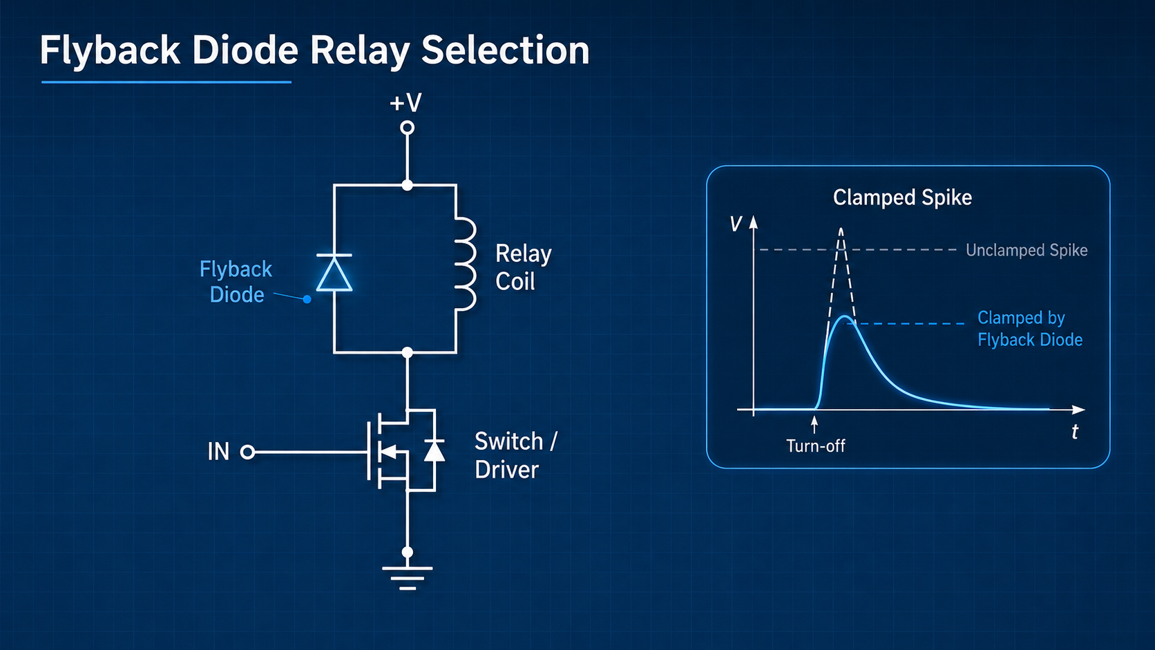 Flyback Diode Relay Selection: How to Choose the Right Diode for a Relay Coil
11 June 2026650
Analog Devices Inc.
In Stock: 4
Minimum: 1 Multiples: 1
Qty
Unit Price
Ext Price
1
$2.273306
$2.27
10
$2.144628
$21.45
100
$2.023234
$202.32
500
$1.908712
$954.36
1000
$1.800671
$1,800.67
Not the price you want? Send RFQ Now and we'll contact you ASAP.
Inquire for More Quantity
![LT1764EQ-3.3#PBF]() LT1764EQ-3.3#PBF
LT1764EQ-3.3#PBFLinear Technology/Analog Devices
![ADP151AUJZ-3.3-R7]() ADP151AUJZ-3.3-R7
ADP151AUJZ-3.3-R7Analog Devices Inc.
![ADP7118AUJZ-5.0-R7]() ADP7118AUJZ-5.0-R7
ADP7118AUJZ-5.0-R7Analog Devices Inc.
![ADP150AUJZ-3.3-R7]() ADP150AUJZ-3.3-R7
ADP150AUJZ-3.3-R7Analog Devices Inc.
![ADP123AUJZ-R7]() ADP123AUJZ-R7
ADP123AUJZ-R7Analog Devices Inc.
![ADM7150ARDZ-5.0]() ADM7150ARDZ-5.0
ADM7150ARDZ-5.0Analog Devices Inc.
![LT1763CS8#TRPBF]() LT1763CS8#TRPBF
LT1763CS8#TRPBFLinear Technology/Analog Devices
![ADP3338AKCZ-2.5RL7]() ADP3338AKCZ-2.5RL7
ADP3338AKCZ-2.5RL7Analog Devices Inc.
![ADP3338AKCZ-3.3RL7]() ADP3338AKCZ-3.3RL7
ADP3338AKCZ-3.3RL7Analog Devices Inc.
![ADP1755ACPZ-R7]() ADP1755ACPZ-R7
ADP1755ACPZ-R7Analog Devices Inc.


