
 Product
 Brand
Brand Articles
 Tools
Tools
TPS92630QPWPRQ1 LED Driver: Pinout, Manufacturer, and Datasheet

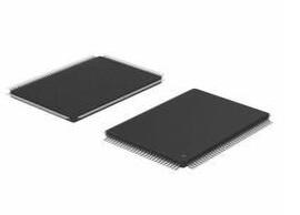
Gold PMIC Automotive, AEC-Q100 Series TPS92630 16 Pin 14V 16-PowerTSSOP (0.173, 4.40mm Width)


Gold PMIC Automotive, AEC-Q100 Series TPS92630 16 Pin 14V 16-PowerTSSOP (0.173, 4.40mm Width)
TPS92630QPWPRQ1 is an Automotive Three-channel Linear LED driver with Analog and PWM dimming. This passage will cover its manufacturer, specification, datasheet, and others.
- TPS92630QPWPRQ1 Description
- TPS92630QPWPRQ1 Application
- TPS92630QPWPRQ1 Application Circiut
- TPS92630QPWPRQ1 CAD Models
- Specifications
- TPS92630QPWPRQ1 Features
- TPS92630QPWPRQ1 Dimensions
- TPS92630QPWPRQ1 Package
- TPS92630QPWPRQ1 Functional Block Diagram
- TPS92630QPWPRQ1 Advantages
- TPS92630QPWPRQ1 Pin Configuration and Functions
- Trend Analysis
- Datasheet PDF
- Parts with Similar Specs
TPS92630QPWPRQ1 Description
The TPS92630QPWPRQ1 is a three-channel constant-current regulator with individual PWM dimming for high-brightness red or white LEDs in vehicle lighting. When paralleled, each channel has a current capability of up to 150 mA, for a total current capability of 450 mA. The device ensures that channels and devices are well-matched in terms of current. LED common-cathode connections are possible with a high-side current source.
Even when differing numbers of LEDs are connected to the output, the complex control loop allows for great precision between channels. Each channel is dimmed or disabled when a separate PWM channel is used.
TPS92630QPWPRQ1 Application
Automotive LED Lighting Applications, Such As:
• Daytime Running Light
• Position Light
• Fog Light
• Rear Light
• Stop or Taillight
• Interior Lighting
TPS92630QPWPRQ1 Application Circiut

TPS92630QPWPRQ1 CAD Models
Symbol

Footprint

3D Models

Specifications
- TypeParameter
- Lifecycle Status
Lifecycle Status refers to the current stage of an electronic component in its product life cycle, indicating whether it is active, obsolete, or transitioning between these states. An active status means the component is in production and available for purchase. An obsolete status indicates that the component is no longer being manufactured or supported, and manufacturers typically provide a limited time frame for support. Understanding the lifecycle status is crucial for design engineers to ensure continuity and reliability in their projects.
ACTIVE (Last Updated: 3 days ago) - Factory Lead Time6 Weeks
- Contact Plating
Contact plating (finish) provides corrosion protection for base metals and optimizes the mechanical and electrical properties of the contact interfaces.
Gold - Mount
In electronic components, the term "Mount" typically refers to the method or process of physically attaching or fixing a component onto a circuit board or other electronic device. This can involve soldering, adhesive bonding, or other techniques to secure the component in place. The mounting process is crucial for ensuring proper electrical connections and mechanical stability within the electronic system. Different components may have specific mounting requirements based on their size, shape, and function, and manufacturers provide guidelines for proper mounting procedures to ensure optimal performance and reliability of the electronic device.
Surface Mount - Mounting Type
The "Mounting Type" in electronic components refers to the method used to attach or connect a component to a circuit board or other substrate, such as through-hole, surface-mount, or panel mount.
Surface Mount - Package / Case
refers to the protective housing that encases an electronic component, providing mechanical support, electrical connections, and thermal management.
16-PowerTSSOP (0.173, 4.40mm Width) - Number of Pins16
- Operating Temperature
The operating temperature is the range of ambient temperature within which a power supply, or any other electrical equipment, operate in. This ranges from a minimum operating temperature, to a peak or maximum operating temperature, outside which, the power supply may fail.
-40°C~125°C TA - Packaging
Semiconductor package is a carrier / shell used to contain and cover one or more semiconductor components or integrated circuits. The material of the shell can be metal, plastic, glass or ceramic.
Tape & Reel (TR) - Series
In electronic components, the "Series" refers to a group of products that share similar characteristics, designs, or functionalities, often produced by the same manufacturer. These components within a series typically have common specifications but may vary in terms of voltage, power, or packaging to meet different application needs. The series name helps identify and differentiate between various product lines within a manufacturer's catalog.
Automotive, AEC-Q100 - JESD-609 Code
The "JESD-609 Code" in electronic components refers to a standardized marking code that indicates the lead-free solder composition and finish of electronic components for compliance with environmental regulations.
e4 - Pbfree Code
The "Pbfree Code" parameter in electronic components refers to the code or marking used to indicate that the component is lead-free. Lead (Pb) is a toxic substance that has been widely used in electronic components for many years, but due to environmental concerns, there has been a shift towards lead-free alternatives. The Pbfree Code helps manufacturers and users easily identify components that do not contain lead, ensuring compliance with regulations and promoting environmentally friendly practices. It is important to pay attention to the Pbfree Code when selecting electronic components to ensure they meet the necessary requirements for lead-free applications.
yes - Part Status
Parts can have many statuses as they progress through the configuration, analysis, review, and approval stages.
Active - Moisture Sensitivity Level (MSL)
Moisture Sensitivity Level (MSL) is a standardized rating that indicates the susceptibility of electronic components, particularly semiconductors, to moisture-induced damage during storage and the soldering process, defining the allowable exposure time to ambient conditions before they require special handling or baking to prevent failures
3 (168 Hours) - Number of Terminations16
- ECCN Code
An ECCN (Export Control Classification Number) is an alphanumeric code used by the U.S. Bureau of Industry and Security to identify and categorize electronic components and other dual-use items that may require an export license based on their technical characteristics and potential for military use.
EAR99 - TypeLinear
- Applications
The parameter "Applications" in electronic components refers to the specific uses or functions for which a component is designed. It encompasses various fields such as consumer electronics, industrial automation, telecommunications, automotive, and medical devices. Understanding the applications helps in selecting the right components for a particular design based on performance, reliability, and compatibility requirements. This parameter also guides manufacturers in targeting their products to relevant markets and customer needs.
Automotive - Terminal Position
In electronic components, the term "Terminal Position" refers to the physical location of the connection points on the component where external electrical connections can be made. These connection points, known as terminals, are typically used to attach wires, leads, or other components to the main body of the electronic component. The terminal position is important for ensuring proper connectivity and functionality of the component within a circuit. It is often specified in technical datasheets or component specifications to help designers and engineers understand how to properly integrate the component into their circuit designs.
DUAL - Terminal Form
Occurring at or forming the end of a series, succession, or the like; closing; concluding.
GULL WING - Peak Reflow Temperature (Cel)
Peak Reflow Temperature (Cel) is a parameter that specifies the maximum temperature at which an electronic component can be exposed during the reflow soldering process. Reflow soldering is a common method used to attach electronic components to a circuit board. The Peak Reflow Temperature is crucial because it ensures that the component is not damaged or degraded during the soldering process. Exceeding the specified Peak Reflow Temperature can lead to issues such as component failure, reduced performance, or even permanent damage to the component. It is important for manufacturers and assemblers to adhere to the recommended Peak Reflow Temperature to ensure the reliability and functionality of the electronic components.
260 - Number of Functions1
- Supply Voltage
Supply voltage refers to the electrical potential difference provided to an electronic component or circuit. It is crucial for the proper operation of devices, as it powers their functions and determines performance characteristics. The supply voltage must be within specified limits to ensure reliability and prevent damage to components. Different electronic devices have specific supply voltage requirements, which can vary widely depending on their design and intended application.
14V - Time@Peak Reflow Temperature-Max (s)
Time@Peak Reflow Temperature-Max (s) refers to the maximum duration that an electronic component can be exposed to the peak reflow temperature during the soldering process, which is crucial for ensuring reliable solder joint formation without damaging the component.
NOT SPECIFIED - Base Part Number
The "Base Part Number" (BPN) in electronic components serves a similar purpose to the "Base Product Number." It refers to the primary identifier for a component that captures the essential characteristics shared by a group of similar components. The BPN provides a fundamental way to reference a family or series of components without specifying all the variations and specific details.
TPS92630 - Number of Outputs3
- Max Output Current
The maximum current that can be supplied to the load.
150mA - Max Supply Voltage
In general, the absolute maximum common-mode voltage is VEE-0.3V and VCC+0.3V, but for products without a protection element at the VCC side, voltages up to the absolute maximum rated supply voltage (i.e. VEE+36V) can be supplied, regardless of supply voltage.
40V - Output Current
The rated output current is the maximum load current that a power supply can provide at a specified ambient temperature. A power supply can never provide more current that it's rated output current unless there is a fault, such as short circuit at the load.
150mA - Max Supply Current
Max Supply Current refers to the maximum amount of electrical current that a component can draw from its power supply under normal operating conditions. It is a critical parameter that ensures the component operates reliably without exceeding its thermal limits or damaging internal circuitry. Exceeding this current can lead to overheating, performance degradation, or failure of the component. Understanding this parameter is essential for designing circuits that provide adequate power while avoiding overload situations.
850μA - Quiescent Current
The quiescent current is defined as the current level in the amplifier when it is producing an output of zero.
600μA - Max Output Voltage
The maximum output voltage refers to the dynamic area beyond which the output is saturated in the positive or negative direction, and is limited according to the load resistance value.
40V - Voltage - Output
Voltage - Output is a parameter that refers to the electrical potential difference between the output terminal or pin of an electronic component and a reference point, typically ground. It indicates the level of voltage that the component is capable of providing at its output under specified operating conditions. This parameter is crucial in determining the performance and functionality of the component in a circuit, as it directly affects the signal or power being delivered to other components or devices connected to the output. Engineers and designers use the voltage output specification to ensure compatibility and proper functioning of the component within the overall system.
4V~75V - Min Input Voltage
The parameter "Min Input Voltage" in electronic components refers to the minimum voltage level that must be applied to the component for it to operate within its specified parameters. This value is crucial as providing a voltage below this minimum threshold may result in the component malfunctioning or not functioning at all. It is important to adhere to the specified minimum input voltage to ensure the proper operation and longevity of the electronic component. Failure to meet this requirement may lead to potential damage to the component or the overall system in which it is used.
5V - Max Input Voltage
Max Input Voltage refers to the maximum voltage level that an electronic component can safely handle without getting damaged. This parameter is crucial for ensuring the proper functioning and longevity of the component. Exceeding the specified maximum input voltage can lead to overheating, electrical breakdown, or permanent damage to the component. It is important to carefully adhere to the manufacturer's guidelines regarding the maximum input voltage to prevent any potential issues and maintain the reliability of the electronic device.
40V - Output Current per Channel
Output Current per Channel is a specification commonly found in electronic components such as amplifiers, audio interfaces, and power supplies. It refers to the maximum amount of electrical current that can be delivered by each individual output channel of the component. This parameter is important because it determines the capacity of the component to drive connected devices or loads. A higher output current per channel means the component can deliver more power to connected devices, while a lower output current may limit the performance or functionality of the component in certain applications. It is crucial to consider the output current per channel when selecting electronic components to ensure they can meet the power requirements of the intended system or setup.
450mA - Internal Switch(s)
The term "Internal Switch(s)" in electronic components typically refers to a built-in mechanism within a device that allows for the control of electrical current flow. These internal switches can be used to turn circuits on or off, change the direction of current, or regulate the flow of electricity within the component. They are often designed to be controlled externally, either manually or automatically, to enable various functions or operations within the electronic device. Internal switches play a crucial role in the overall functionality and performance of electronic components by providing a means to manage and manipulate electrical signals effectively.
Yes - Dimming
Dimming is a feature in electronic components, such as LED lights or display screens, that allows the user to adjust the brightness level of the device. It is a method of controlling the amount of light output by the component, typically by varying the voltage or current supplied to it. Dimming can be achieved through various techniques, such as pulse-width modulation (PWM) or analog dimming. This feature is commonly used to save energy, create ambiance, or enhance visual comfort in different applications.
Analog, PWM - Min Input Voltage (DC)
Min Input Voltage (DC) refers to the minimum direct current (DC) voltage that an electronic component or device requires to operate properly. This parameter is crucial for ensuring that the component receives enough power to function within its specified operating range. If the input voltage falls below the minimum threshold, the component may not function correctly or may not operate at all. It is important to adhere to the specified minimum input voltage to prevent damage to the component and ensure reliable performance.
5V - Number of Segments7
- Multiplexed Display Capability
Multiplexed Display Capability refers to the ability of an electronic component or system to control multiple display elements using fewer input/output lines. This is achieved by rapidly switching between different displays or segments, allowing for efficient communication and reduced wiring complexity. In multiplexed systems, each display is activated sequentially, creating the illusion of simultaneous display to the user. This capability is commonly utilized in devices like LED matrices and LCD screens to enhance functionality while conserving space and resources.
NO - Height1.2mm
- Length5mm
- Width4.4mm
- Thickness
Thickness in electronic components refers to the measurement of how thick a particular material or layer is within the component structure. It can pertain to various aspects, such as the thickness of a substrate, a dielectric layer, or conductive traces. This parameter is crucial as it impacts the electrical, mechanical, and thermal properties of the component, influencing its performance and reliability in electronic circuits.
1mm - RoHS Status
RoHS means “Restriction of Certain Hazardous Substances” in the “Hazardous Substances Directive” in electrical and electronic equipment.
ROHS3 Compliant - Lead Free
Lead Free is a term used to describe electronic components that do not contain lead as part of their composition. Lead is a toxic material that can have harmful effects on human health and the environment, so the electronics industry has been moving towards lead-free components to reduce these risks. Lead-free components are typically made using alternative materials such as silver, copper, and tin. Manufacturers must comply with regulations such as the Restriction of Hazardous Substances (RoHS) directive to ensure that their products are lead-free and environmentally friendly.
Lead Free
TPS92630QPWPRQ1 Features
Qualified for Automotive Applications
AEC-Q100 Qualified With the Following Results:
– Device Temperature Grade 1: –40°C to 125 °C Ambient Operating Temperature Range
– Device HBM ESD Classification Level H2
– Device CDM ESD Classification Level C3B
3-Ch. LED Driver With Analog and PWM Dimming
Wide Input-Voltage Range: 5 V–40 V
Adjustable Constant Output Current Set by reference Resistor
– Max. Current: 150 mA per Channel
– Max. Current: 450 mA in Parallel Operation Mode
– Accuracy: ±1.5% per Channel When I(IOUTx) > 30 mA
– Accuracy: ±2.5% per Device When I(IOUTx) > 30 mA
Parallel Outputs for Higher Current Using MultipleICs or Multiple Channels of a Single IC
Low Dropout Voltage
– Max. Dropout: 40 0 mV at 60 mA per Channel
– Max. Dropout: 0.9 V at 150 mA per Channel
Independent PWM Dimming per Channel
Open and Shorted LED Detection With DeglitchTimer
LED-String Voltage Feedback per Channel for single-LED Short Detection
Separate Fault Pin for Single-LED Short Failure
Fault Pin for Open, Short, and Thermal ShutdownFailure Reporting, Allowing Parallel Bus Connection up to 15 Devices
Device Accommodates a Slow Input-Voltage dV/dt(0.5 V/min) With No Issues
Operating Junction Temperature Range –40°C to150°C
Package: 16-Pin Thermally Enhanced PWP Package (HTSSOP)
TPS92630QPWPRQ1 Dimensions
| Height | 1.2mm |
| Length | 5mm |
| Thickness | 1mm |
| Width | 4.4mm |
TPS92630QPWPRQ1 Package
TPS92630QPWPRQ1 Functional Block Diagram

TPS92630QPWPRQ1 Advantages
Constant LED -Current Setting
Control of the three LED output channels is through separate linear current regulators. A common external resistor sets the current in each channel.
The device features a separate PWM dimming control pin for each output channel. PWM inputs also function as shutdown pins when output is unused.
FAULT Diagnostics
The TPS92630QPWPRQ1 device has two fault pins, FAULT and FAULT _S. FAULT _S is a dedicated fault pin for the single LED short failure and FAULT is for general faults, that is, short, open, and thermal shutdown.
Short-Circuit Detection
The device includes three internal comparators for LED forward-voltage measurement. With external resistor dividers, the device compares total LED forward voltage with the internal reference voltage. This feature enables the detection of one or more shorted LED s.
Open-Load Detection
Detection of an open-load condition occurs when the voltage across the channel, V(VIN) – V(IOUTx), is less than the open-load detection voltage, V(OLV)
Thermal Foldback
The TPS92630-Q1 device integrates thermal shutdown protection to prevent the device from overheating.
TPS92630QPWPRQ1 Pin Configuration and Functions

| PIN | |||
| Name | NO. | I/O | DESCRIPTION |
| EN | 2 | I | Enable and shut down |
| FAULT | 6 | I/O | Fault pin. Leave floating if not used |
| FAULT_S | 7 | I/O | Single-LED short fault. Leave floating if not used |
| GND | 10 | - | Ground |
| IOUT1 | 16 | O | Current output pin. Connect to VSNS1 if not used. |
| IOUT2 | 15 | O | Current output pin. Connect to VSNS2 if not used. |
| IOUT3 | 14 | O | Current output pin. Connect to VSNS3 if not used. |
| PWM1 | 3 | I | PWM input and channel ON or OFF. Tie to GND if this channel is not used |
| PWM2 | 4 | I | PWM input and channel ON or OFF. Tie to GND if this channel is not used |
| PWM3 | 5 | I | PWM input and channel ON or OFF. Tie to GND if this channel is not used |
| REF | 9 | O | Reference resistor pin for the normal current setting |
| TEMP | 8 | I/O | Temperature foldback threshold program. Tie to GND if not used. |
| VIN | 1 | Input pin – VBAT supply | |
| VSNS1 | 11 | String voltage sense. Connect to IOUT1 if not used | |
| VSNS2 | 12 | String voltage sense. Connect to IOUT2 if not used | |
| VSNS3 | 13 | String voltage sense. Connect to IOUT3 if not used | |
| Thermal pad | - | - | Connect to GND |
Trend Analysis
Datasheet PDF
- PCN Design/Specification :
Parts with Similar Specs
- ImagePart NumberManufacturerPackage / CaseNumber of PinsNumber of OutputsMin Input VoltageMin Input Voltage (DC)Max Input VoltageMax Output CurrentOutput CurrentMax Output VoltageView Compare
![TPS92630QPWPRQ1]()
TPS92630QPWPRQ1
16-PowerTSSOP (0.173, 4.40mm Width)
16
3
5 V
5 V
40 V
150 mA
150 mA
40 V
![LM3532TMX-40A/NOPB]()
16-VFQFN Exposed Pad
16
3
2.7 V
-
6.5 V
75 mA
75 mA
-
![LV5217GP-TE-L-E]()
16-WFBGA, DSBGA
16
3
-
-
-
-
-
-
![TPS60231RGTR]()
16-WFQFN
16
3
-
-
-
-
-
-
![FAN5616MPX]()
16-WFQFN Exposed Pad
16
3
-
-
-
-
-
-


What’s the recommended operating conditions?
VIN is between 5 and 40v. PWMx, EN, and VSNSx are between 0 and 40v. FAULT and FAULT-S are between 0 and 20v. Others are between 0 and 5v.
What is TPS92630QPWPRQ1?
The TPS92630QPWPRQ1device is a three-channel linear LED driver with analog and PWM dimming control. Its full-diagnostic and built-in protection capabilities make it a suitable choice for variable-intensity LED lighting applications up to the medium-power range.
How many pins does LP5018RSMR have?
16
Can TPS92630QPWPRQ1 be operated in 100℃?
Yes, its operating junction temperature range is from -40 to 150℃.
In order to reduce the damage, what should we pay attention to?
First, TJ must be less than 150℃. If the input voltage is very high, the power dissipation might be large.
Secondly, The devices are currently available in the TSSOP-EP package, which has good thermal impedance.
Thirdly,  the PCB layout is also very important. Good PCB design can optimize heat transfer.
 AD9508 1.65 GHz Clock Buffer: Datasheet, Ultra-Low Jitter Specs, and Configuration Analysis
21 April 2026275
 KSZ8895MQXI Ethernet Switch SPI Interface 128-PQFP: Datasheet, Pinout, and equivalent
11 February 20222131
 STM32H743: Detailed Datasheet, Pinout, and Alternatives Guide
23 January 20267501
 BC550 NPN Transistor: Pinout, Datasheet, and Equivalents
18 August 20217808
 SP0503BAHT TVS Diode Arrays: Circuit, Pinout, and Datasheet
25 February 20223746
 MAX6675 Type-K Thermocouple Converter : Datasheet, Pinout, Comparison
14 September 202111331
 STWD100NYWY3F: ST, Watchdog Timer Circuit, STWD100NYWY3F PDF
05 January 20222225
 TE Connectivity 1-968855-1 Terminal: Complete Automotive Wiring Guide
28 August 2025193
 Introduction to FinFET
18 March 202130169
 Top 10 Technology Trends in the Global Semiconductor Industry in 2022
08 January 20229260
 What is the Difference between MOM, MIM and MOS Capacitors?
17 April 202569301
 What is a Thyristor?
11 December 202012109
 Bridge Rectifier: Functions, Circuits and Applications
03 November 202015631
 Introduction to TFT Displays
29 August 20209567
 The Proactive Playbook for EOL Component Sourcing: Managing NRND Without Adding Risk
09 June 2026143
 Analyzing Temperature Parameters of Si, SiC and GaN Power Devices
09 September 20231489
Texas Instruments
In Stock: 18323
United States
China
Canada
Japan
Russia
Germany
United Kingdom
Singapore
Italy
Hong Kong(China)
Taiwan(China)
France
Korea
Mexico
Netherlands
Malaysia
Austria
Spain
Switzerland
Poland
Thailand
Vietnam
India
United Arab Emirates
Afghanistan
Åland Islands
Albania
Algeria
American Samoa
Andorra
Angola
Anguilla
Antigua & Barbuda
Argentina
Armenia
Aruba
Australia
Azerbaijan
Bahamas
Bahrain
Bangladesh
Barbados
Belarus
Belgium
Belize
Benin
Bermuda
Bhutan
Bolivia
Bonaire, Sint Eustatius and Saba
Bosnia & Herzegovina
Botswana
Brazil
British Indian Ocean Territory
British Virgin Islands
Brunei
Bulgaria
Burkina Faso
Burundi
Cabo Verde
Cambodia
Cameroon
Cayman Islands
Central African Republic
Chad
Chile
Christmas Island
Cocos (Keeling) Islands
Colombia
Comoros
Congo
Congo (DRC)
Cook Islands
Costa Rica
Côte d’Ivoire
Croatia
Cuba
Curaçao
Cyprus
Czechia
Denmark
Djibouti
Dominica
Dominican Republic
Ecuador
Egypt
El Salvador
Equatorial Guinea
Eritrea
Estonia
Eswatini
Ethiopia
Falkland Islands
Faroe Islands
Fiji
Finland
French Guiana
French Polynesia
Gabon
Gambia
Georgia
Ghana
Gibraltar
Greece
Greenland
Grenada
Guadeloupe
Guam
Guatemala
Guernsey
Guinea
Guinea-Bissau
Guyana
Haiti
Honduras
Hungary
Iceland
Indonesia
Iran
Iraq
Ireland
Isle of Man
Israel
Jamaica
Jersey
Jordan
Kazakhstan
Kenya
Kiribati
Kosovo
Kuwait
Kyrgyzstan
Laos
Latvia
Lebanon
Lesotho
Liberia
Libya
Liechtenstein
Lithuania
Luxembourg
Macao(China)
Madagascar
Malawi
Maldives
Mali
Malta
Marshall Islands
Martinique
Mauritania
Mauritius
Mayotte
Micronesia
Moldova
Monaco
Mongolia
Montenegro
Montserrat
Morocco
Mozambique
Myanmar
Namibia
Nauru
Nepal
New Caledonia
New Zealand
Nicaragua
Niger
Nigeria
Niue
Norfolk Island
North Korea
North Macedonia
Northern Mariana Islands
Norway
Oman
Pakistan
Palau
Palestinian Authority
Panama
Papua New Guinea
Paraguay
Peru
Philippines
Pitcairn Islands
Portugal
Puerto Rico
Qatar
Réunion
Romania
Rwanda
Samoa
San Marino
São Tomé & Príncipe
Saudi Arabia
Senegal
Serbia
Seychelles
Sierra Leone
Sint Maarten
Slovakia
Slovenia
Solomon Islands
Somalia
South Africa
South Sudan
Sri Lanka
St Helena, Ascension, Tristan da Cunha
St. Barthélemy
St. Kitts & Nevis
St. Lucia
St. Martin
St. Pierre & Miquelon
St. Vincent & Grenadines
Sudan
Suriname
Svalbard & Jan Mayen
Sweden
Syria
Tajikistan
Tanzania
Timor-Leste
Togo
Tokelau
Tonga
Trinidad & Tobago
Tunisia
Turkey
Turkmenistan
Turks & Caicos Islands
Tuvalu
U.S. Outlying Islands
U.S. Virgin Islands
Uganda
Ukraine
Uruguay
Uzbekistan
Vanuatu
Vatican City
Venezuela
Wallis & Futuna
Yemen
Zambia
Zimbabwe
![UCC25710DWR]() UCC25710DWR
UCC25710DWRTexas Instruments
![LM3447MTX/NOPB]() LM3447MTX/NOPB
LM3447MTX/NOPBTexas Instruments
![TPS61040DBVR]() TPS61040DBVR
TPS61040DBVRTexas Instruments
![TPS61041DBVR]() TPS61041DBVR
TPS61041DBVRTexas Instruments
![TPS61165DRVR]() TPS61165DRVR
TPS61165DRVRTexas Instruments
![LM3409HVMY/NOPB]() LM3409HVMY/NOPB
LM3409HVMY/NOPBTexas Instruments
![TLC59116IRHBR]() TLC59116IRHBR
TLC59116IRHBRTexas Instruments
![TLC5971PWPR]() TLC5971PWPR
TLC5971PWPRTexas Instruments
![TLC5940PWPR]() TLC5940PWPR
TLC5940PWPRTexas Instruments
![TLC5922DAP]() TLC5922DAP
TLC5922DAPTexas Instruments


