

 Product
 Brand
Brand Articles
 Tools
Tools
USB3300 Transceiver: Features, Pinout, and Datasheet [Video&FAQ]

3V~3.6V USB 2.0, OTG ULPI Controllers Interface ICs QUAD USB3300 32 Pins Controller 32-VFQFN Exposed Pad


3V~3.6V USB 2.0, OTG ULPI Controllers Interface ICs QUAD USB3300 32 Pins Controller 32-VFQFN Exposed Pad
The USB3300 is a high-speed USB Physical Layer Transceiver that can withstand extreme temperatures (PHY). This article mainly introduces Features, Pinout, Datasheet and other detailed information about Microchip Technology USB3300.

Cheap USB Host Microcontroller [CH559, ESP32, HID]
USB3300 Description
The USB3300 is a high-speed USB Physical Layer Transceiver that can withstand extreme temperatures (PHY). To connect to a ULPI-compliant Link layer, the USB3300 uses a low pin count interface (ULPI). Using in-band signaling and status byte transfers between the Link and PHY, the ULPI interface reduces the UTMI+ interface from 54 to 12 pins.
The ULPI interface was built into this PHY from the ground up. This design does not use any UTMI to ULPI wrappers, resulting in a smooth ULPI to Link interface. As a result, a PHY with reduced transmit and receive latency has been developed. Microchip's low latency high speed and full speed receivers allow current UTMI Links to be converted to ULPI via a simple wrapper.
The USB3300 PHY can be used as a device, a host, or an On-The-Go (OTG) device thanks to the ULPI interface. With no additional pins, designs employing the USB3300 PHY as a device can add host and OTG functionality later.
The USB3300 is the best way to incorporate Hi-Speed USB into new designs because to its ULPI interface and Microchip's patented technologies. The USB3300 has an industry-leading tiny footprint packaging (5mm by 5mm) and a height of less than 1mm. Furthermore, the USB3300 includes all DP and DM termination resistances and only requires a few extra components.
USB3300 Pinout
With a via array to the ground plane, the exposed flag of the QFN package must be linked to the ground. This is the USB3300's main ground connection.

Pinout
| Pin Number | Pin Name | Description |
| 1 | GND | Ground |
| 2 | GND | Ground |
| 3 | CPEN | External 5 volt supply enable. This pin is used to enable the external Vbus power supply. The CPEN pin is low on POR. |
| 4 | VBUS | VBUS pin of the USB cable. The USB3300 uses this pin for the Vbus comparator inputs and for Vbus pulsing during session request protocol. |
| 5 | ID | ID pin of the USB cable. For non-OTG applications this pin can be floated. For an A-Device ID = 0. For a B-Device ID = 1. |
| 6 | VDD3.3 | 3.3V Supply. A 0.1uF bypass capacitor should be connected between this pin and the ground plane on the PCB. |
| 7 | DP | D+ pin of the USB cable. |
| 8 | DM | D- pin of the USB cable. |
| 9 | RESET | Optional active high transceiver reset. This is the same as a write to the ULPI Reset, address 04h, bit 5. This does not reset the ULPI register set. This pin includes an integrated pull-down resistor to ground. If not used, this pin can be floated or connected to ground (recommended). |
| 10 | EXTVBUS | External Vbus Detect. Connect to fault output of an external USB power switch or an external Vbus Valid comparator. This pin has a pull down resistor to prevent it from floating when the ULPI bit UseExternalVbusIndicator is set to 0. |
| 11 | NXT | The PHY asserts NXT to throttle the data. When the Link is sending data to the PHY, NXT indicates when the current byte has been accepted by the PHY. The Link places the next byte on the data bus in the following clock cycle. |
| 12 | DIR | Controls the direction of the data bus. When the PHY has data to transfer to the Link, it drives DIR high to take ownership of the bus. When the PHY has no data to transfer it drives DIR low and monitors the bus for commands from the Link. The PHY will pull DIR high whenever the interface cannot accept data from the Link, such as during PLL start-up. |
| 13 | STP | The Link asserts STP for one clock cycle to stop the data stream currently on the bus. If the Link is sending data to the PHY, STP indicates the last byte of data was on the bus in the previous cycle. |
| 14 | CLKOUT | 60MHz reference clock output. All ULPI signals are driven synchronous to the rising edge of this clock. |
| 15 | VDD1.8 | 1.8V for digital circuitry on chip. Supplied by On-Chip Regulator when REG_EN is active. Place a 0.1uF capacitor near this pin and connect the capacitor from this pin to ground. Connect pin 15 to pin 26. |
| 16 | VDD3.3 | A 0.1uF bypass capacitor should be connected between this pin and the ground plane on the PCB. |
| 17 | DATA[7] | 8-bit bi-directional data bus. Bus ownership is determined by DIR. The Link and PHY initiate data transfers by driving a non-zero pattern onto the data bus. ULPI defines interface timing for a single-edge data transfers with respect to rising edge of CLKOUT. DATA[7] is the MSB and DATA[0] is the LSB. |
| 18 | DATA[6] | |
| 19 | DATA[5] | |
| 20 | DATA[4] | |
| 21 | DATA[3] | |
| 22 | DATA[2] | |
| 23 | DATA[1] | |
| 24 | DATA[0] | |
| 25 | VDD3.3 | A 0.1uF bypass capacitor should be connected between this pin and the ground plane on the PCB. |
| 26 | VDD1.8 | 1.8V for digital circuitry on chip. Supplied by On-Chip Regulator when REG_EN is active. When using the internal regulators, place a 4.7uF low-ESR capacitor near this pin and connect the capacitor from this pin to ground. Connect pin 26 to pin 15. Do not connect VDD1.8 to VDDA1.8 when using internal regulators. When the regulators are disabled, pin 29 may be connected to pins 26 and 15. |
| 27 | XO | Crystal pin. If using an external clock on XI this pin should be floated. |
| 28 | XI | Crystal pin. A 24MHz crystal is supported. The crystal is placed across XI and XO. An external 24MHz clock source may be driven into XI in place of a crystal. |
| 29 | VDDA1.8 | 1.8V for analog circuitry on chip. Supplied by On-Chip Regulator when REG_EN is active. Place a 0.1uF capacitor near this pin and connect the capacitor from this pin to ground. When using the internal regulators, place a 4.7uF low-ESR capacitor near this pin in parallel with the 0.1uF capacitor. Do not connect VDD1.8A to VDD1.8 when using internal regulators. When the regulators are disabled, pin 29 may be connected to pins 26 and 15. |
| 30 | VDD3.3 | Analog 3.3 volt supply. A 0.1uF low ESR bypass capacitor connected to the ground plane of the PCB is recommended. |
| 31 | REG_EN | On-Chip 1.8V regulator enable. Connect to ground to disable both of the on chip (VDDA1.8 and VDD1.8) regulators. When regulators are disabled: • External 1.8V must be supplied to VDDA1.8 and VDD1.8 pins. When the regulators are disabled, VDDA1.8 may be connected to VDD1.8 and a bypass capacitor (0.1uF recommended) should be connected to each pin. • The voltage at VDD3.3 must be at least 2.64V (0.8 * 3.3V) before voltage is applied to VDDA1.8 and VDD1.8. |
| 32 | RBIAS | External 12KΩ +/- 1% bias resistor to ground. |
| GND FLAG | Ground. The flag must be connected to the ground plane with a via array under the exposed flag. This is the main ground for the IC. |
USB3300 CAD Model

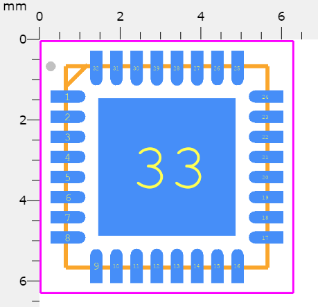
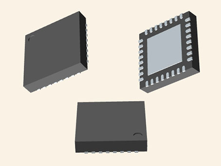
USB3300 Features
• USB-IF Hi-Speed certified to the Universal Serial Bus Specification Rev 2.0
• Interface compliant with the ULPI Specification revision 1.1 in 8-bit mode
• Industry standard UTMI+ Low Pin Interface (ULPI) Converts 54 UTMI+ signals into a standard 12 pin Link controller interface
• 54.7mA Unconfigured Current (typical) - ideal for bus powered applications
• 83uA suspend current (typical) - ideal for battery powered applications
• Latch-Up performance exceeds 150 mA per EIA /JESD 78, Class II
• ESD protection levels of ±8kV HBM without external protection devices
• Integrated protection to withstand IEC61000-4-2 ESD tests (±8kV contact and ±15kV air) per 3rd party test facility
• Supports FS preamble for FS hubs with a LS device attached (UTMI+ Level 3)
• Supports HS SOF and LS keep-alive pulse
• Includes full support for the optional On-The-Go (OTG) protocol detailed in the On-The-Go Supplement Revision 1.0a specification
• Supports the OTG Host Negotiation Protocol (HNP) and Session Request Protocol (SRP)
• Allows host to turn VBUS off to conserve battery power in OTG applications
• Supports OTG monitoring of VBUS levels with internal comparators. Includes support for an external VBUS or fault monitor.
• Low Latency Hi-Speed Receiver (43 Hi-Speed clocks Max) allows use of legacy UTMI Links with a ULPI wrapper
• Integrated Pull-up resistor on STP for interface protection allows a reliable Link/PHY start-up with slow Links (software configured for low power)
• Internal 1.8 volt regulators allow operation from a single 3.3 volt supply
• Internal short circuit protection of ID, DP and DM lines to VBUS or ground
• Integrated 24MHz Crystal Oscillator supports either crystal operation or 24MHz external clock input
• Internal PLL for 480MHz Hi-Speed USB operation
• Industrial Operating Temperature -40°C to +85°C
• 32 pin, QFN RoHS Compliant package (5 x 5 x 0.90 mm height)
Specifications
- TypeParameter
- Factory Lead Time11 Weeks
- Contact Plating
Contact plating (finish) provides corrosion protection for base metals and optimizes the mechanical and electrical properties of the contact interfaces.
Tin - Mount
In electronic components, the term "Mount" typically refers to the method or process of physically attaching or fixing a component onto a circuit board or other electronic device. This can involve soldering, adhesive bonding, or other techniques to secure the component in place. The mounting process is crucial for ensuring proper electrical connections and mechanical stability within the electronic system. Different components may have specific mounting requirements based on their size, shape, and function, and manufacturers provide guidelines for proper mounting procedures to ensure optimal performance and reliability of the electronic device.
Surface Mount - Package / Case
refers to the protective housing that encases an electronic component, providing mechanical support, electrical connections, and thermal management.
32-VFQFN Exposed Pad - Number of Pins32
- Weight188.609377mg
- Usage LevelIndustrial grade
- Operating Temperature
The operating temperature is the range of ambient temperature within which a power supply, or any other electrical equipment, operate in. This ranges from a minimum operating temperature, to a peak or maximum operating temperature, outside which, the power supply may fail.
-40°C~85°C - Packaging
Semiconductor package is a carrier / shell used to contain and cover one or more semiconductor components or integrated circuits. The material of the shell can be metal, plastic, glass or ceramic.
Tray - Published2005
- JESD-609 Code
The "JESD-609 Code" in electronic components refers to a standardized marking code that indicates the lead-free solder composition and finish of electronic components for compliance with environmental regulations.
e3 - Pbfree Code
The "Pbfree Code" parameter in electronic components refers to the code or marking used to indicate that the component is lead-free. Lead (Pb) is a toxic substance that has been widely used in electronic components for many years, but due to environmental concerns, there has been a shift towards lead-free alternatives. The Pbfree Code helps manufacturers and users easily identify components that do not contain lead, ensuring compliance with regulations and promoting environmentally friendly practices. It is important to pay attention to the Pbfree Code when selecting electronic components to ensure they meet the necessary requirements for lead-free applications.
yes - Part Status
Parts can have many statuses as they progress through the configuration, analysis, review, and approval stages.
Active - Moisture Sensitivity Level (MSL)
Moisture Sensitivity Level (MSL) is a standardized rating that indicates the susceptibility of electronic components, particularly semiconductors, to moisture-induced damage during storage and the soldering process, defining the allowable exposure time to ambient conditions before they require special handling or baking to prevent failures
3 (168 Hours) - Number of Terminations32
- Voltage - Supply
Voltage - Supply refers to the range of voltage levels that an electronic component or circuit is designed to operate with. It indicates the minimum and maximum supply voltage that can be applied for the device to function properly. Providing supply voltages outside this range can lead to malfunction, damage, or reduced performance. This parameter is critical for ensuring compatibility between different components in a circuit.
3V~3.6V - Terminal Position
In electronic components, the term "Terminal Position" refers to the physical location of the connection points on the component where external electrical connections can be made. These connection points, known as terminals, are typically used to attach wires, leads, or other components to the main body of the electronic component. The terminal position is important for ensuring proper connectivity and functionality of the component within a circuit. It is often specified in technical datasheets or component specifications to help designers and engineers understand how to properly integrate the component into their circuit designs.
QUAD - Peak Reflow Temperature (Cel)
Peak Reflow Temperature (Cel) is a parameter that specifies the maximum temperature at which an electronic component can be exposed during the reflow soldering process. Reflow soldering is a common method used to attach electronic components to a circuit board. The Peak Reflow Temperature is crucial because it ensures that the component is not damaged or degraded during the soldering process. Exceeding the specified Peak Reflow Temperature can lead to issues such as component failure, reduced performance, or even permanent damage to the component. It is important for manufacturers and assemblers to adhere to the recommended Peak Reflow Temperature to ensure the reliability and functionality of the electronic components.
260 - Supply Voltage
Supply voltage refers to the electrical potential difference provided to an electronic component or circuit. It is crucial for the proper operation of devices, as it powers their functions and determines performance characteristics. The supply voltage must be within specified limits to ensure reliability and prevent damage to components. Different electronic devices have specific supply voltage requirements, which can vary widely depending on their design and intended application.
3.3V - Time@Peak Reflow Temperature-Max (s)
Time@Peak Reflow Temperature-Max (s) refers to the maximum duration that an electronic component can be exposed to the peak reflow temperature during the soldering process, which is crucial for ensuring reliable solder joint formation without damaging the component.
40 - Base Part Number
The "Base Part Number" (BPN) in electronic components serves a similar purpose to the "Base Product Number." It refers to the primary identifier for a component that captures the essential characteristics shared by a group of similar components. The BPN provides a fundamental way to reference a family or series of components without specifying all the variations and specific details.
USB3300 - Function
The parameter "Function" in electronic components refers to the specific role or purpose that the component serves within an electronic circuit. It defines how the component interacts with other elements, influences the flow of electrical signals, and contributes to the overall behavior of the system. Functions can include amplification, signal processing, switching, filtering, and energy storage, among others. Understanding the function of each component is essential for designing effective and efficient electronic systems.
Controller - Voltage
Voltage is a measure of the electric potential difference between two points in an electrical circuit. It is typically represented by the symbol "V" and is measured in volts. Voltage is a crucial parameter in electronic components as it determines the flow of electric current through a circuit. It is responsible for driving the movement of electrons from one point to another, providing the energy needed for electronic devices to function properly. In summary, voltage is a fundamental concept in electronics that plays a key role in the operation and performance of electronic components.
5V - Interface
In electronic components, the term "Interface" refers to the point at which two different systems, devices, or components connect and interact with each other. It can involve physical connections such as ports, connectors, or cables, as well as communication protocols and standards that facilitate the exchange of data or signals between the connected entities. The interface serves as a bridge that enables seamless communication and interoperability between different parts of a system or between different systems altogether. Designing a reliable and efficient interface is crucial in ensuring proper functionality and performance of electronic components and systems.
ULPI - Operating Supply Current
Operating Supply Current, also known as supply current or quiescent current, is a crucial parameter in electronic components that indicates the amount of current required for the device to operate under normal conditions. It represents the current drawn by the component from the power supply while it is functioning. This parameter is important for determining the power consumption of the component and is typically specified in datasheets to help designers calculate the overall power requirements of their circuits. Understanding the operating supply current is essential for ensuring proper functionality and efficiency of electronic systems.
54.7mA - Number of Ports
A port is identified for each transport protocol and address combination by a 16-bit unsigned number,.
1 - Data Rate
Data Rate is defined as the amount of data transmitted during a specified time period over a network. It is the speed at which data is transferred from one device to another or between a peripheral device and the computer. It is generally measured in Mega bits per second(Mbps) or Mega bytes per second(MBps).
480 Mbps - Protocol
In electronic components, the parameter "Protocol" refers to a set of rules and standards that govern the communication between devices. It defines the format, timing, sequencing, and error checking methods for data exchange between different components or systems. Protocols ensure that devices can understand and interpret data correctly, enabling them to communicate effectively with each other. Common examples of protocols in electronics include USB, Ethernet, SPI, I2C, and Bluetooth, each with its own specifications for data transmission. Understanding and adhering to protocols is essential for ensuring compatibility and reliable communication between electronic devices.
USB - Telecom IC Type
Telecom IC Type refers to integrated circuits specifically designed for telecommunications applications. These components facilitate various functions such as signal processing, data modulation and demodulation, and communication protocol handling. They can be used in devices like mobile phones, modems, and network equipment, ensuring reliable data transmission and reception. Telecom ICs support different standards and technologies, making them essential for modern communication systems.
INTERFACE CIRCUIT - ESD Protection
ESD protection, or Electrostatic Discharge protection, is a feature in electronic components designed to prevent damage caused by sudden electrostatic discharges. These discharges can occur when a person or object with an electric charge comes into contact with a sensitive electronic component, leading to a rapid flow of static electricity that can damage or destroy the component. ESD protection mechanisms in electronic components typically involve the use of special materials or circuitry that can safely dissipate or divert the excess charge away from the sensitive components, thus safeguarding the device from potential harm. Implementing effective ESD protection is crucial in ensuring the reliability and longevity of electronic devices, especially in environments where static electricity buildup is common, such as in manufacturing facilities or areas with low humidity.
Yes - USB
USB stands for Universal Serial Bus, which is a common interface used for connecting various electronic devices to a computer or other host device. It allows for the transfer of data, power, and communication between devices. USB ports are found on a wide range of devices such as computers, smartphones, printers, cameras, and more. The USB standard has evolved over the years to include different versions with varying data transfer speeds and power delivery capabilities. Overall, USB has become a widely adopted and versatile standard for connecting and interacting with electronic components.
USB 2.0 - Standards
The parameter "Standards" in electronic components refers to established criteria or specifications that ensure interoperability, safety, and performance across various electronic devices and systems. These standards are often set by recognized organizations and describe the characteristics, dimensions, and testing methods for components. Adherence to these standards helps manufacturers produce compatible and reliable products, facilitates communication between devices, and ensures compliance with regulatory requirements. Standards play a crucial role in the consistency and quality of electronic components in the industry.
USB 2.0, OTG - Ambient Temperature Range High
This varies from person to person, but it is somewhere between 68 and 77 degrees F on average. The temperature setting that is comfortable for an individual may fluctuate with humidity and outside temperature as well. The temperature of an air conditioned room can also be considered ambient temperature.
85°C - Height1mm
- Length5mm
- Width5mm
- REACH SVHC
The parameter "REACH SVHC" in electronic components refers to the compliance with the Registration, Evaluation, Authorization, and Restriction of Chemicals (REACH) regulation regarding Substances of Very High Concern (SVHC). SVHCs are substances that may have serious effects on human health or the environment, and their use is regulated under REACH to ensure their safe handling and minimize their impact.Manufacturers of electronic components need to declare if their products contain any SVHCs above a certain threshold concentration and provide information on the safe use of these substances. This information allows customers to make informed decisions about the potential risks associated with using the components and take appropriate measures to mitigate any hazards.Ensuring compliance with REACH SVHC requirements is essential for electronics manufacturers to meet regulatory standards, protect human health and the environment, and maintain transparency in their supply chain. It also demonstrates a commitment to sustainability and responsible manufacturing practices in the electronics industry.
No SVHC - Radiation Hardening
Radiation hardening is the process of making electronic components and circuits resistant to damage or malfunction caused by high levels of ionizing radiation, especially for environments in outer space (especially beyond the low Earth orbit), around nuclear reactors and particle accelerators, or during nuclear accidents or nuclear warfare.
No - RoHS Status
RoHS means “Restriction of Certain Hazardous Substances” in the “Hazardous Substances Directive” in electrical and electronic equipment.
ROHS3 Compliant - Lead Free
Lead Free is a term used to describe electronic components that do not contain lead as part of their composition. Lead is a toxic material that can have harmful effects on human health and the environment, so the electronics industry has been moving towards lead-free components to reduce these risks. Lead-free components are typically made using alternative materials such as silver, copper, and tin. Manufacturers must comply with regulations such as the Restriction of Hazardous Substances (RoHS) directive to ensure that their products are lead-free and environmentally friendly.
Lead Free
Parts with Similar Specs
- ImagePart NumberManufacturerPackage / CaseNumber of PinsInterfaceNumber of PortsData RateSupply VoltageRoHS StatusMountView Compare
![USB3300-EZK]()
USB3300-EZK
32-VFQFN Exposed Pad
32
ULPI
1
480 Mbps
3.3 V
ROHS3 Compliant
Surface Mount
![USB3343-CP]()
24-VFQFN Exposed Pad
24
UART, USB
1
480 Mbps
1.8 V
ROHS3 Compliant
Surface Mount
![78Q2123/F]()
28-VFQFN Exposed Pad
28
-
2
480 Mbps
3.3 V
ROHS3 Compliant
Surface Mount
![USB2422-I/MJ]()
32-VFQFN Exposed Pad
32
-
-
100 Mbps
3.3 V
ROHS3 Compliant
Surface Mount
![USB2412-DZK]()
24-VFQFN Exposed Pad
24
-
-
480 Mbps
3.3 V
ROHS3 Compliant
Surface Mount


USB3300 Functional Block Diagram
The USB3300 is a USB PHY with a lot of features. It includes a comprehensive Hi-Speed USB 2.0 PHY with the ULPI industry-standard interface to help you get your USB device to market quickly.

Functional Block Diagram
USB3300 Application Diagrams
The followings are USB3300 Application Diagrams.
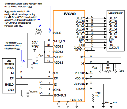
Application Diagram (Peripheral)
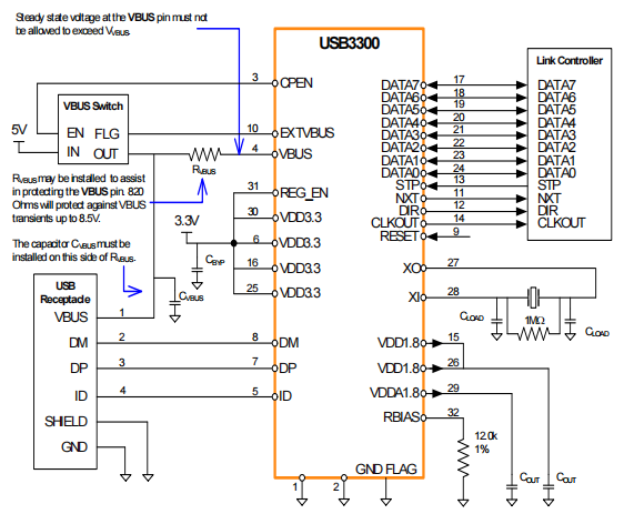
Application Diagram (HOST or OTG)
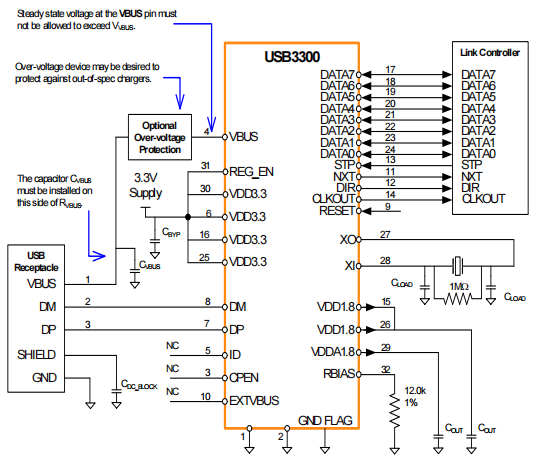
Application Diagram (Peripheral with Over-voltage Protection)
USB3300 Alternatives
| Part Number | Description | Manufacturer |
| USB3300-EZK-TRTELECOMMUNICATION CIRCUITS | DATACOM, INTERFACE CIRCUIT, QCC32, 5 X 5 MM, 0.90 MM HEIGHT, ROHS COMPLIANT, QFN-32 | Microchip Technology Inc |
| USB3300-EZKTELECOMMUNICATION CIRCUITS | DATACOM, INTERFACE CIRCUIT, QCC32, 5 X 5 MM, 0.90 MM HEIGHT, ROHS COMPLIANT, QFN-32 | Microchip Technology Inc |
| USB3300I-EZK-TRTELECOMMUNICATION CIRCUITS | DATACOM, INTERFACE CIRCUIT | Microchip Technology Inc |
USB3300 Applications
The USB3300 is the ideal companion to any ASIC, SoC or FPGA solution designed with a ULPI Hi-Speed USB host, peripheral or OTG core.
The USB3300 is well suited for:
• Cell Phones
• PDAs
• MP3 Players
• Scanners
• External Hard Drives
• Digital Still and Video Cameras
• Portable Media Players
• Printers
USB3300 Package
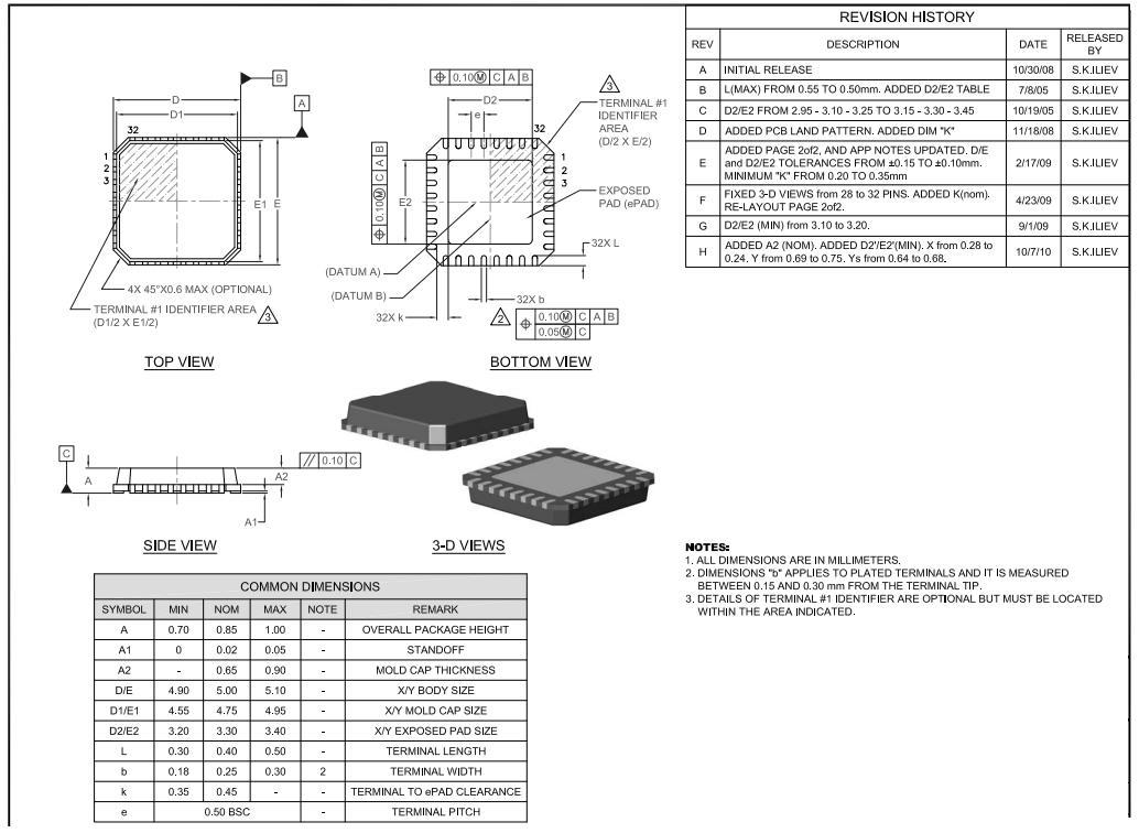
USB3300 Manufacturer
Microchip Technology Incorporated is a leading manufacturer of smart, networked, and secure embedded control solutions. Customers may create optimal designs using the company's simple development tools and broad product choices, which reduce risk while lowering overall system costs and time to market. The company's technologies are used by over 120,000 clients in the industrial, automotive, consumer, aerospace and defense, communications, and computing sectors. Microchip Technology Inc., based in Chandler, Arizona, offers outstanding technical assistance as well as reliable delivery and quality.
Trend Analysis
Datasheet PDF
- PCN Design/Specification :
- PCN Packaging :
- ConflictMineralStatement :
- Datasheets :
What is the USB3300?
A high-speed USB Physical Layer Transceiver.
What does the USB3300 use to connect to a ULPI-compliant Link layer?
Low pin count interface.
How many pins does the ULPI interface reduce the UTMI+ interface?
54 to 12 pins.
What interface was built into the USB3300 from the ground up?
ULPI.
What type of PHY has been developed?
Reduced transmit and receive latency.
What does the USB3300 PHY do with no additional pins?
Add host and OTG functionality later.
What is the best way to incorporate the USB3300 PHY into new designs?
Hi-Speed USB.
What is the size of the USB3300?
5mm by 5mm.
What types of termination resistances does the USB3300 include?
DP and DM termination resistances.
 In-Depth Analysis of the Microchip PIC16F873/874/876/877 Microcontrollers
29 February 2024479
 NTE987 Operational Amplifier: Datasheet, Pinout and Equivalent
16 September 20212609
 AT90CAN32 Microcontroller: Pinout, Equivalent and Datasheet
23 February 20221563
 TPS92515QDGQRQ1 LED Drivers: Equivalence, Datasheet, and Pinout
21 March 20221799
 TL431CLP IC Adjustable ±2.2% 100 mA TO-92-3: Datasheet, Pinout, and Schematic
03 March 2022483
 AT28C256 Paged Parallel EEPROM: Pinout, Equivalent and Datasheet
21 April 20224106
 A Comprehensive Guide to the AD558 Digital to Analog Converter (DAC)
06 March 20241040
 MJE13007 NPN Bipolar Power Transistor: Equivalent, Datasheet and Pinout
22 October 202129214
 Semiconductor R&D Spending: Top 12 Countries
20 September 20233791
 Domestic SSD Master Chip Maker, Achieving a New Breakthrough in PCIe 5.0
27 April 2022708
 Ceramic Capacitor Failure Mode and Mechanism Analysis
21 May 202213942
 HDMI RF Modulators: Architecture, Setup, Types, and Commercial Applications
18 May 2026343
 What is DDR5 SDRAM? The Ultimate Guide to Specs, Architecture, and Market Trends
05 January 202611637
 The Practical Engineer’s Guide to the NE555N Timer: Pinout, Setup, and Troubleshooting
29 May 2026288
 Optical Gates for High-Speed Optical Processing Using Semiconductor-Based Amplifiers
30 December 20222043
 nF Capacitors: Definition, Conversion, Circuit Applications, and Selection
12 August 20257721
Microchip Technology
In Stock: 490
United States
China
Canada
Japan
Russia
Germany
United Kingdom
Singapore
Italy
Hong Kong(China)
Taiwan(China)
France
Korea
Mexico
Netherlands
Malaysia
Austria
Spain
Switzerland
Poland
Thailand
Vietnam
India
United Arab Emirates
Afghanistan
Åland Islands
Albania
Algeria
American Samoa
Andorra
Angola
Anguilla
Antigua & Barbuda
Argentina
Armenia
Aruba
Australia
Azerbaijan
Bahamas
Bahrain
Bangladesh
Barbados
Belarus
Belgium
Belize
Benin
Bermuda
Bhutan
Bolivia
Bonaire, Sint Eustatius and Saba
Bosnia & Herzegovina
Botswana
Brazil
British Indian Ocean Territory
British Virgin Islands
Brunei
Bulgaria
Burkina Faso
Burundi
Cabo Verde
Cambodia
Cameroon
Cayman Islands
Central African Republic
Chad
Chile
Christmas Island
Cocos (Keeling) Islands
Colombia
Comoros
Congo
Congo (DRC)
Cook Islands
Costa Rica
Côte d’Ivoire
Croatia
Cuba
Curaçao
Cyprus
Czechia
Denmark
Djibouti
Dominica
Dominican Republic
Ecuador
Egypt
El Salvador
Equatorial Guinea
Eritrea
Estonia
Eswatini
Ethiopia
Falkland Islands
Faroe Islands
Fiji
Finland
French Guiana
French Polynesia
Gabon
Gambia
Georgia
Ghana
Gibraltar
Greece
Greenland
Grenada
Guadeloupe
Guam
Guatemala
Guernsey
Guinea
Guinea-Bissau
Guyana
Haiti
Honduras
Hungary
Iceland
Indonesia
Iran
Iraq
Ireland
Isle of Man
Israel
Jamaica
Jersey
Jordan
Kazakhstan
Kenya
Kiribati
Kosovo
Kuwait
Kyrgyzstan
Laos
Latvia
Lebanon
Lesotho
Liberia
Libya
Liechtenstein
Lithuania
Luxembourg
Macao(China)
Madagascar
Malawi
Maldives
Mali
Malta
Marshall Islands
Martinique
Mauritania
Mauritius
Mayotte
Micronesia
Moldova
Monaco
Mongolia
Montenegro
Montserrat
Morocco
Mozambique
Myanmar
Namibia
Nauru
Nepal
New Caledonia
New Zealand
Nicaragua
Niger
Nigeria
Niue
Norfolk Island
North Korea
North Macedonia
Northern Mariana Islands
Norway
Oman
Pakistan
Palau
Palestinian Authority
Panama
Papua New Guinea
Paraguay
Peru
Philippines
Pitcairn Islands
Portugal
Puerto Rico
Qatar
Réunion
Romania
Rwanda
Samoa
San Marino
São Tomé & Príncipe
Saudi Arabia
Senegal
Serbia
Seychelles
Sierra Leone
Sint Maarten
Slovakia
Slovenia
Solomon Islands
Somalia
South Africa
South Sudan
Sri Lanka
St Helena, Ascension, Tristan da Cunha
St. Barthélemy
St. Kitts & Nevis
St. Lucia
St. Martin
St. Pierre & Miquelon
St. Vincent & Grenadines
Sudan
Suriname
Svalbard & Jan Mayen
Sweden
Syria
Tajikistan
Tanzania
Timor-Leste
Togo
Tokelau
Tonga
Trinidad & Tobago
Tunisia
Turkey
Turkmenistan
Turks & Caicos Islands
Tuvalu
U.S. Outlying Islands
U.S. Virgin Islands
Uganda
Ukraine
Uruguay
Uzbekistan
Vanuatu
Vatican City
Venezuela
Wallis & Futuna
Yemen
Zambia
Zimbabwe
![KSZ8895MQXIA]() KSZ8895MQXIA
KSZ8895MQXIAMicrochip Technology
![USB2514BI-AEZG]() USB2514BI-AEZG
USB2514BI-AEZGMicrochip Technology
![USB2514B-AEZC-TR]() USB2514B-AEZC-TR
USB2514B-AEZC-TRMicrochip Technology
![MCP2515-I/ST]() MCP2515-I/ST
MCP2515-I/STMicrochip Technology
![MCP2515-I/SO]() MCP2515-I/SO
MCP2515-I/SOMicrochip Technology
![ENC28J60-I/SS]() ENC28J60-I/SS
ENC28J60-I/SSMicrochip Technology
![KSZ8873MMLI]() KSZ8873MMLI
KSZ8873MMLIMicrochip Technology
![MCP2200-I/SO]() MCP2200-I/SO
MCP2200-I/SOMicrochip Technology
![KSZ8863RLLI]() KSZ8863RLLI
KSZ8863RLLIMicrochip Technology
![KSZ8863MLL]() KSZ8863MLL
KSZ8863MLLMicrochip Technology


