
 Product
 Brand
Brand Articles
 Tools
Tools
Where & How to Use CA3240 Dual Op Amp? [FAQ]

Renesas Electronics America Inc.
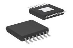
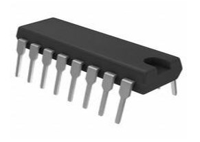
10pA 90 dB Instrumentational OP Amps 4V~36V ±2V~18V CA3240 8 Pins 8-DIP (0.300, 7.62mm)


10pA 90 dB Instrumentational OP Amps 4V~36V ±2V~18V CA3240 8 Pins 8-DIP (0.300, 7.62mm)
The CA3240 is a dual version of the popular CA3140 series integrated circuit operational amplifiers. This article will introduce CA3240 systematically from its features, pinout to its specifications, applications, also including CA3240 datasheet and so much more. Furthermore, Huge range of Semiconductors, Capacitors, Resistors and IcS in stock. Welcome RFQ.

How OpAmps Work - The Learning Circuit
CA3240 Pinout
The following figure is the diagram of CA3240 Pinout.

Pinout
CA3240 CAD Model
The followings are CA3240 Symbol, Footprint, and 3D Model.

PCB Symbol

PCB Footprint

3D Model
CA3240 Overview
The CA3240 is a dual version of the popular CA3140 series integrated circuit operational amplifiers. CD3240 combines the advantages of MOS and bipolar transistors on the same monolithic chip. The gate-protected MOSFET input transistors provide high input impedance and a wide common-mode input voltage range (typically to 0.5V below the negative supply rail).
This article provides you with a basic overview of the CA3240 Dual Operational Amplifier, including its pin descriptions, features and specifications, etc., to help you quickly understand what CA3240 is.
CA3240 Features
● Number of Channels: 2 Channel
● Can work from a single power supply
● GBP - Gain Bandwidth Product: 4.5 MHz
● Supply Voltage - Max: 36 V
● Supply Voltage - Min: 4 V
● Maximum Dual Supply Voltage: +/- 18 V
● Minimum Dual Supply Voltage: +/- 2 V
● Operating Supply Current: 8 mA
● Output Current per Channel: 40 mA
● SR - Slew Rate: 9 V/us
● CMRR - Common Mode Rejection Ratio: 70 dB
● Vos - Input Offset Voltage: 15 mV
Specifications
- TypeParameter
- Factory Lead Time12 Weeks
- Mounting Type
The "Mounting Type" in electronic components refers to the method used to attach or connect a component to a circuit board or other substrate, such as through-hole, surface-mount, or panel mount.
Through Hole - Package / Case
refers to the protective housing that encases an electronic component, providing mechanical support, electrical connections, and thermal management.
8-DIP (0.300, 7.62mm) - Surface Mount
having leads that are designed to be soldered on the side of a circuit board that the body of the component is mounted on.
NO - Usage LevelIndustrial grade
- Operating Temperature
The operating temperature is the range of ambient temperature within which a power supply, or any other electrical equipment, operate in. This ranges from a minimum operating temperature, to a peak or maximum operating temperature, outside which, the power supply may fail.
-40°C~85°C - Packaging
Semiconductor package is a carrier / shell used to contain and cover one or more semiconductor components or integrated circuits. The material of the shell can be metal, plastic, glass or ceramic.
Tube - Published1998
- JESD-609 Code
The "JESD-609 Code" in electronic components refers to a standardized marking code that indicates the lead-free solder composition and finish of electronic components for compliance with environmental regulations.
e3 - Part Status
Parts can have many statuses as they progress through the configuration, analysis, review, and approval stages.
Active - Moisture Sensitivity Level (MSL)
Moisture Sensitivity Level (MSL) is a standardized rating that indicates the susceptibility of electronic components, particularly semiconductors, to moisture-induced damage during storage and the soldering process, defining the allowable exposure time to ambient conditions before they require special handling or baking to prevent failures
1 (Unlimited) - Number of Terminations8
- Terminal Finish
Terminal Finish refers to the surface treatment applied to the terminals or leads of electronic components to enhance their performance and longevity. It can improve solderability, corrosion resistance, and overall reliability of the connection in electronic assemblies. Common finishes include nickel, gold, and tin, each possessing distinct properties suitable for various applications. The choice of terminal finish can significantly impact the durability and effectiveness of electronic devices.
Matte Tin (Sn) - annealed - Terminal Position
In electronic components, the term "Terminal Position" refers to the physical location of the connection points on the component where external electrical connections can be made. These connection points, known as terminals, are typically used to attach wires, leads, or other components to the main body of the electronic component. The terminal position is important for ensuring proper connectivity and functionality of the component within a circuit. It is often specified in technical datasheets or component specifications to help designers and engineers understand how to properly integrate the component into their circuit designs.
DUAL - Number of Functions2
- Supply Voltage
Supply voltage refers to the electrical potential difference provided to an electronic component or circuit. It is crucial for the proper operation of devices, as it powers their functions and determines performance characteristics. The supply voltage must be within specified limits to ensure reliability and prevent damage to components. Different electronic devices have specific supply voltage requirements, which can vary widely depending on their design and intended application.
15V - Base Part Number
The "Base Part Number" (BPN) in electronic components serves a similar purpose to the "Base Product Number." It refers to the primary identifier for a component that captures the essential characteristics shared by a group of similar components. The BPN provides a fundamental way to reference a family or series of components without specifying all the variations and specific details.
CA3240 - Pin Count
a count of all of the component leads (or pins)
8 - JESD-30 Code
JESD-30 Code refers to a standardized descriptive designation system established by JEDEC for semiconductor-device packages. This system provides a systematic method for generating designators that convey essential information about the package's physical characteristics, such as size and shape, which aids in component identification and selection. By using JESD-30 codes, manufacturers and engineers can ensure consistency and clarity in the specification of semiconductor packages across various applications and industries.
R-PDIP-T8 - Number of Circuits2
- Current - Supply
Current - Supply is a parameter in electronic components that refers to the maximum amount of electrical current that the component can provide to the circuit it is connected to. It is typically measured in units of amperes (A) and is crucial for determining the power handling capability of the component. Understanding the current supply rating is important for ensuring that the component can safely deliver the required current without overheating or failing. It is essential to consider this parameter when designing circuits to prevent damage to the component and ensure proper functionality of the overall system.
8mA - Slew Rate
the maximum rate of output voltage change per unit time.
9V/μs - Amplifier Type
Amplifier Type refers to the classification or categorization of amplifiers based on their design, functionality, and characteristics. Amplifiers are electronic devices that increase the amplitude of a signal, such as voltage or current. The type of amplifier determines its specific application, performance capabilities, and operating characteristics. Common types of amplifiers include operational amplifiers (op-amps), power amplifiers, audio amplifiers, and radio frequency (RF) amplifiers. Understanding the amplifier type is crucial for selecting the right component for a particular circuit or system design.
General Purpose - Common Mode Rejection Ratio
Common Mode Rejection Ratio (CMRR) is a measure of the ability of a differential amplifier to reject input signals that are common to both input terminals. It is defined as the ratio of the differential gain to the common mode gain. A high CMRR indicates that the amplifier can effectively eliminate noise and interference that affects both inputs simultaneously, enhancing the fidelity of the amplified signal. CMRR is typically expressed in decibels (dB), with higher values representing better performance in rejecting common mode signals.
90 dB - Current - Input Bias
The parameter "Current - Input Bias" in electronic components refers to the amount of current required at the input terminal of a device to maintain proper operation. It is a crucial specification as it determines the minimum input current needed for the component to function correctly. Input bias current can affect the performance and accuracy of the device, especially in precision applications where small signal levels are involved. It is typically specified in datasheets for operational amplifiers, transistors, and other semiconductor devices to provide users with important information for circuit design and analysis.
10pA - Voltage - Supply, Single/Dual (±)
The parameter "Voltage - Supply, Single/Dual (±)" in electronic components refers to the power supply voltage required for the proper operation of the component. This parameter indicates whether the component requires a single power supply voltage (e.g., 5V) or a dual power supply voltage (e.g., ±15V). For components that require a single power supply voltage, only one voltage level is needed for operation. On the other hand, components that require a dual power supply voltage need both positive and negative voltage levels to function correctly.Understanding the voltage supply requirements of electronic components is crucial for designing and integrating them into circuits to ensure proper functionality and prevent damage due to incorrect voltage levels.
4V~36V ±2V~18V - Neg Supply Voltage-Nom (Vsup)
The parameter "Neg Supply Voltage-Nom (Vsup)" in electronic components refers to the nominal negative supply voltage that the component requires to operate within its specified performance characteristics. This parameter indicates the minimum voltage level that must be provided to the component's negative supply pin for proper functionality. It is important to ensure that the negative supply voltage provided to the component does not exceed the maximum specified value to prevent damage or malfunction. Understanding and adhering to the specified negative supply voltage requirements is crucial for the reliable operation of the electronic component in a circuit.
-15V - Unity Gain BW-Nom
Unity Gain Bandwidth, often abbreviated as Unity Gain BW or UGBW, refers to the frequency at which an amplifier can provide a gain of one (0 dB). It is a critical parameter in assessing the performance of operational amplifiers and other amplifying devices, indicating the range of frequencies over which the amplifier can operate without distortion. Unity Gain BW is particularly important in applications where signal fidelity is crucial, as it helps determine the maximum frequency of operation for a given gain level. As the gain is reduced, the bandwidth typically increases, ensuring that the amplifier can still operate effectively across various signal frequencies.
4500 kHz - Supply Voltage Limit-Max
The parameter "Supply Voltage Limit-Max" in electronic components refers to the maximum voltage that the component can safely handle without getting damaged. This specification is crucial for ensuring the reliable operation and longevity of the component within a given electrical system. Exceeding the maximum supply voltage limit can lead to overheating, electrical breakdown, or permanent damage to the component. It is important to carefully adhere to this limit when designing and operating electronic circuits to prevent potential failures and ensure the overall system's performance and safety.
18V - Voltage - Input Offset
Voltage - Input Offset is a parameter that refers to the difference in voltage between the input terminals of an electronic component, such as an operational amplifier, when the input voltage is zero. It is an important characteristic that can affect the accuracy and performance of the component in various applications. A low input offset voltage is desirable as it indicates that the component will have minimal error in its output when the input signal is near zero. Manufacturers typically provide this specification in the component's datasheet to help users understand the component's behavior and make informed decisions when designing circuits.
5mV - Neg Supply Voltage-Max (Vsup)
Neg Supply Voltage-Max (Vsup) refers to the maximum negative supply voltage that an electronic component can tolerate without being damaged. It indicates the lowest voltage level that can be applied to the negative supply pin of the device. Exceeding this parameter can lead to functional failure or permanent damage to the component. This specification is crucial for ensuring proper operation and preventing circuit malfunction in designs that utilize negative voltage supplies.
-18V - RoHS Status
RoHS means “Restriction of Certain Hazardous Substances” in the “Hazardous Substances Directive” in electrical and electronic equipment.
ROHS3 Compliant
CA3240 Functional Block Diagram
The following is the Functional Diagram of CA3240.

Functional Diagram
The following diagram shows the CA3240 Schematic Diagram (One Amplifier of Two).
.png")
Schematic Diagram (One Amplifier of Two)
Where to Use CA3240 Op Amp?
CA3240 IC can be used to realize general-purpose op-amp operation circuits like comparator, differential amplification or mathematical operations. Moreover, the device specifically designed for applications like transducer amplifiers, dc amplification blocks to be implemented more easily in single-supply-voltage systems. For example, these devices can be operated directly from the standard 5V supply used in digital electronics without additional -5V supply.
In addition with two of those op-amps on board, the device can perform two different functions at a time that comes in handy in applications. The device is popular among hobbyists and engineers for being low cost and good performance.
How to Use CA3240 Op Amp IC?
As mentioned above CA3240 is a dual op-amp IC. The internal connection diagram of CA3240 is shown below.

Now let us take a single op-amp from the two and construct a simple application circuit as shown below.

In the above circuit, the op-amp acts as a Non-Inverting Amplifier (Since the input is given to the Non-inverting terminal of the op-amp) and output is provided as Vo. Also, the device is powered from a single voltage source of VCC.
We have the equation for the output Vo =Input voltage * Gain = Vi * A = Vi * (1+R1/R2)
For example:
Say R1 = 100, R2 = 10 and Input voltage Vi = 20mV
We will have Vo = 20m*(1+10)=220mV
With that, we have realized the amplifier circuit of the op-amp and in a similar way, we use the device to design all other application circuits of an op-amp.
Similar Op-Amp. ICs
LM158, LM158A, LM358, LM358A, LM2904, LM2904Q, LM4558, LM747
CA3240 Applications
● Ground Referenced Single Amplifiers in Automobile and Portable Instrumentation
● Sample and Hold Amplifiers
● Long Duration Timers/Multivibrators (Microseconds Minutes-Hours)
● Photocurrent Instrumentation
● Intrusion Alarm System
● Comparators
● Instrumentation Amplifiers
● Active Filters
● Function Generators
● Power Supplies
Using Warning
Note: Please check their parameters and pin configuration before replacing them in your circuit.
CA3240 Manufacturer
Renesas Electronics Corporation is a Japanese semiconductor manufacturer headquartered in Tokyo, Japan, initially incorporated in 2002 as Renesas Technology, the consolidated entity of the semiconductor units of Hitachi and Mitsubishi excluding their dynamic random-access memory businesses, to which NEC Electronics merged in 2010, resulting in a minor change in the corporate name and logo to as it is now.
Renesas Electronics delivers trusted embedded design innovation with complete semiconductor solutions that enable billions of connected, intelligent devices to enhance the way people work and live - securely and safely.The number one global supplier of microcontrollers, and a leader in Analog & Power and SoC products, Renesas provides the expertise, quality, and comprehensive solutions for a broad range of Automotive, Industrial, Home Electronics (HE), Office Automation (OA) and Information Communication Technology (ICT) applications to help shape a limitless future.
Datasheet PDF
- Datasheets :
- ConflictMineralStatement :
How many pins of CA3240EZ?
8 Pins.
What’s the operating temperature of CA3240EZ?
-40°C~85°C.
What is Bimos operational amplifier?
w/MOSFET Input, Bipolar Output. Description: The NTE7144 is an integrated circuit operational amplifier in an 8–Lead Mini–DIP type package that combines the advantages of high–voltage PMOS transistors with high–voltage bipolar transistors on a single monolithic chip.
What is operational amplifier?
An operational amplifier is an integrated circuit that can amplify weak electric signals. An operational amplifier has two input pins and one output pin. Its basic role is to amplify and output the voltage difference between the two input pins.
Why is it called operational amplifier?
Originally, op-amps were so named because they were used to model the basic mathematical operations of addition, subtraction, integration, differentiation, etc. in electronic analog computers. In this sense a true operational amplifier is an ideal circuit element.
 AD843 CBFET Series 250 V/µs Op-Amp: High-Speed Performance and Stability Analysis
28 February 202642
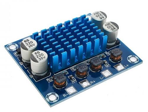 What you need to know about TPA3110 Bluetooth Audio Power Amplifier Board
26 April 202216758
 LM317K 1.2V TO 37V VOLTAGE REGULATOR:Pinout, Datasheet, and Applications
14 September 20212624
![BT152-800R,127 Thyristor: Pinout, Datasheet, Application [FAQ]](https://res.utmel.com/Images/Article/8573419c-625e-4147-8b0e-f9a35c2cdd6e.jpg) BT152-800R,127 Thyristor: Pinout, Datasheet, Application [FAQ]
BT152-800R,127 Thyristor: Pinout, Datasheet, Application [FAQ]27 April 20227951
 TXS0108EPWR: Applications, Features and Datasheet
18 October 20231233
 TPS1H100AQPWPRQ1 High-Side Power Switch: Features, Pinout, and Datasheet
26 March 2022319
![LS14500 3.6 V AA Lithium Battery 2.6 Ah[Video+FAQ]](https://res.utmel.com/Images/Article/e56d6782-c55e-4720-a448-6da3b6402280.png) LS14500 3.6 V AA Lithium Battery 2.6 Ah[Video+FAQ]
LS14500 3.6 V AA Lithium Battery 2.6 Ah[Video+FAQ]23 April 2022379
 ULN2001A Transistor Array: Pinout, Equivalent and Datasheet
30 November 20212459
 How much do you know about Button Battery?
15 March 20244768
 Elon Musk: The Neuralink Brain Chip Developed By Its Company Could Help Treat Morbid Obesity
24 April 20222257
 Utmel Customer Rating Standard, Rights and Interests
24 July 20203682
 Power Converter with Inbuilt Charging technology using WBG Devices
18 January 20242207
 13 kinds of sensors in mobile phones and what are recorded by the sensors
26 November 2025117539
 Selection Criteria for Power Management ICs (PMICs)
06 April 20223396
 What are the Types and Dielectric of Ceramic Capacitors?
16 October 202511351
 The History of Thermometers
09 January 202616544
Renesas Electronics America Inc.
In Stock
United States
China
Canada
Japan
Russia
Germany
United Kingdom
Singapore
Italy
Hong Kong(China)
Taiwan(China)
France
Korea
Mexico
Netherlands
Malaysia
Austria
Spain
Switzerland
Poland
Thailand
Vietnam
India
United Arab Emirates
Afghanistan
Åland Islands
Albania
Algeria
American Samoa
Andorra
Angola
Anguilla
Antigua & Barbuda
Argentina
Armenia
Aruba
Australia
Azerbaijan
Bahamas
Bahrain
Bangladesh
Barbados
Belarus
Belgium
Belize
Benin
Bermuda
Bhutan
Bolivia
Bonaire, Sint Eustatius and Saba
Bosnia & Herzegovina
Botswana
Brazil
British Indian Ocean Territory
British Virgin Islands
Brunei
Bulgaria
Burkina Faso
Burundi
Cabo Verde
Cambodia
Cameroon
Cayman Islands
Central African Republic
Chad
Chile
Christmas Island
Cocos (Keeling) Islands
Colombia
Comoros
Congo
Congo (DRC)
Cook Islands
Costa Rica
Côte d’Ivoire
Croatia
Cuba
Curaçao
Cyprus
Czechia
Denmark
Djibouti
Dominica
Dominican Republic
Ecuador
Egypt
El Salvador
Equatorial Guinea
Eritrea
Estonia
Eswatini
Ethiopia
Falkland Islands
Faroe Islands
Fiji
Finland
French Guiana
French Polynesia
Gabon
Gambia
Georgia
Ghana
Gibraltar
Greece
Greenland
Grenada
Guadeloupe
Guam
Guatemala
Guernsey
Guinea
Guinea-Bissau
Guyana
Haiti
Honduras
Hungary
Iceland
Indonesia
Iran
Iraq
Ireland
Isle of Man
Israel
Jamaica
Jersey
Jordan
Kazakhstan
Kenya
Kiribati
Kosovo
Kuwait
Kyrgyzstan
Laos
Latvia
Lebanon
Lesotho
Liberia
Libya
Liechtenstein
Lithuania
Luxembourg
Macao(China)
Madagascar
Malawi
Maldives
Mali
Malta
Marshall Islands
Martinique
Mauritania
Mauritius
Mayotte
Micronesia
Moldova
Monaco
Mongolia
Montenegro
Montserrat
Morocco
Mozambique
Myanmar
Namibia
Nauru
Nepal
New Caledonia
New Zealand
Nicaragua
Niger
Nigeria
Niue
Norfolk Island
North Korea
North Macedonia
Northern Mariana Islands
Norway
Oman
Pakistan
Palau
Palestinian Authority
Panama
Papua New Guinea
Paraguay
Peru
Philippines
Pitcairn Islands
Portugal
Puerto Rico
Qatar
Réunion
Romania
Rwanda
Samoa
San Marino
São Tomé & Príncipe
Saudi Arabia
Senegal
Serbia
Seychelles
Sierra Leone
Sint Maarten
Slovakia
Slovenia
Solomon Islands
Somalia
South Africa
South Sudan
Sri Lanka
St Helena, Ascension, Tristan da Cunha
St. Barthélemy
St. Kitts & Nevis
St. Lucia
St. Martin
St. Pierre & Miquelon
St. Vincent & Grenadines
Sudan
Suriname
Svalbard & Jan Mayen
Sweden
Syria
Tajikistan
Tanzania
Timor-Leste
Togo
Tokelau
Tonga
Trinidad & Tobago
Tunisia
Turkey
Turkmenistan
Turks & Caicos Islands
Tuvalu
U.S. Outlying Islands
U.S. Virgin Islands
Uganda
Ukraine
Uruguay
Uzbekistan
Vanuatu
Vatican City
Venezuela
Wallis & Futuna
Yemen
Zambia
Zimbabwe
![HA1630Q06TELL-E]() HA1630Q06TELL-E
HA1630Q06TELL-ERenesas Electronics America
![HA1630D06TEL-E]() HA1630D06TEL-E
HA1630D06TEL-ERenesas Electronics America
![UPC3218GV-E1-A]() UPC3218GV-E1-A
UPC3218GV-E1-ARenesas
![UPC3221GV-E1-A]() UPC3221GV-E1-A
UPC3221GV-E1-ARenesas
![UPC842G2-E2-A]() UPC842G2-E2-A
UPC842G2-E2-ARenesas
![PS8551L4-E3-AX]() PS8551L4-E3-AX
PS8551L4-E3-AXRenesas Electronics America
![ISL28236FUZ-T7]() ISL28236FUZ-T7
ISL28236FUZ-T7Renesas Electronics America Inc.
![UPC834G2-E2-A]() UPC834G2-E2-A
UPC834G2-E2-ARenesas
![ISL28158FHZ-T7A]() ISL28158FHZ-T7A
ISL28158FHZ-T7ARenesas Electronics America Inc.
![HA1630D06MMEL-E]() HA1630D06MMEL-E
HA1630D06MMEL-ERenesas Electronics America


