
 Product
 Brand
Brand Articles
 Tools
Tools
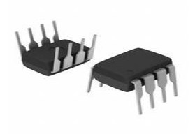
CA3140 Op-Amp: Circuit, Pinout and Datasheet

Intersil (Renesas Electronics America)
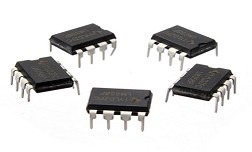
40mA per Channel 10pA 90 dB Instrumentational OP Amps 9V 8 Pins DIP


40mA per Channel 10pA 90 dB Instrumentational OP Amps 9V 8 Pins DIP
CA3140 is a 4.5MHz, BiMOS Operational Amplifier with MOSFET Input/Bipolar Output. This article mainly introduce its circuit, pinout, datasheet and other detailed information about Intersil CA3140.

How to Make Efficient Automatic Street Light System using IC CA3140 (Op Amp)
CA3140 Description
The CA3140 is integrated circuit operation amplifier combining the advantages of high voltage PMOS transistor with high voltage bipolar transistor single chip. CA3140 BiMOS operational amplifier MOSFET (PMOS) transistor with gate protection The input circuit provides very high input impedance, very low Input current and high-speed performance. CA3140 operates with a supply voltage of 4V to 36V (single power supply or dual power supply). These op amps Internal phase compensation for stability The unity gain follows the operation in operation, in addition, access terminal with auxiliary external capacitor If additional frequency roll-off is required. terminal too provided for applications that require input offset voltage Zero. The use of PMOS field effect tube at the input end phase causes the common mode input voltage capability to drop 0.5V below the negative power supply terminal, an important
The properties of a single power supply application. Output stage uses bipolar transistors and includes built-in protection prevent damage caused by short-circuit of load terminals to either end power rail or ground. CA3140 for power supply operation The voltage is up to 36V (±18V).
CA3140 Pinout

CA3140 CAD Model
Symbol

Footprint

3D Model

CA3140 Features
• MOSFET input stage
-Very high input impedance (ZIN) -1.5TΩ (typical value)
-Very low input current (Il) -10pA (typical value), ±15V
-Wide common mode input voltage range (VlCR)-Can be swung 0.5V below the negative supply voltage rail
-Output swing supplements input common mode range
• Replace the industry type 741 directly in most applications
• Pb-free plus anneal available (compliant with RoHS)
Specifications
- TypeParameter
- Contact Plating
Contact plating (finish) provides corrosion protection for base metals and optimizes the mechanical and electrical properties of the contact interfaces.
Lead, Tin - Mount
In electronic components, the term "Mount" typically refers to the method or process of physically attaching or fixing a component onto a circuit board or other electronic device. This can involve soldering, adhesive bonding, or other techniques to secure the component in place. The mounting process is crucial for ensuring proper electrical connections and mechanical stability within the electronic system. Different components may have specific mounting requirements based on their size, shape, and function, and manufacturers provide guidelines for proper mounting procedures to ensure optimal performance and reliability of the electronic device.
Through Hole - Package / Case
refers to the protective housing that encases an electronic component, providing mechanical support, electrical connections, and thermal management.
DIP - Number of Pins8
- Published1998
- JESD-609 Code
The "JESD-609 Code" in electronic components refers to a standardized marking code that indicates the lead-free solder composition and finish of electronic components for compliance with environmental regulations.
e0 - Pbfree Code
The "Pbfree Code" parameter in electronic components refers to the code or marking used to indicate that the component is lead-free. Lead (Pb) is a toxic substance that has been widely used in electronic components for many years, but due to environmental concerns, there has been a shift towards lead-free alternatives. The Pbfree Code helps manufacturers and users easily identify components that do not contain lead, ensuring compliance with regulations and promoting environmentally friendly practices. It is important to pay attention to the Pbfree Code when selecting electronic components to ensure they meet the necessary requirements for lead-free applications.
no - ECCN Code
An ECCN (Export Control Classification Number) is an alphanumeric code used by the U.S. Bureau of Industry and Security to identify and categorize electronic components and other dual-use items that may require an export license based on their technical characteristics and potential for military use.
EAR99 - Terminal Finish
Terminal Finish refers to the surface treatment applied to the terminals or leads of electronic components to enhance their performance and longevity. It can improve solderability, corrosion resistance, and overall reliability of the connection in electronic assemblies. Common finishes include nickel, gold, and tin, each possessing distinct properties suitable for various applications. The choice of terminal finish can significantly impact the durability and effectiveness of electronic devices.
Tin/Lead (Sn/Pb) - Max Operating Temperature
The Maximum Operating Temperature is the maximum body temperature at which the thermistor is designed to operate for extended periods of time with acceptable stability of its electrical characteristics.
125°C - Min Operating Temperature
The "Min Operating Temperature" parameter in electronic components refers to the lowest temperature at which the component is designed to operate effectively and reliably. This parameter is crucial for ensuring the proper functioning and longevity of the component, as operating below this temperature may lead to performance issues or even damage. Manufacturers specify the minimum operating temperature to provide guidance to users on the environmental conditions in which the component can safely operate. It is important to adhere to this parameter to prevent malfunctions and ensure the overall reliability of the electronic system.
-55°C - Terminal Position
In electronic components, the term "Terminal Position" refers to the physical location of the connection points on the component where external electrical connections can be made. These connection points, known as terminals, are typically used to attach wires, leads, or other components to the main body of the electronic component. The terminal position is important for ensuring proper connectivity and functionality of the component within a circuit. It is often specified in technical datasheets or component specifications to help designers and engineers understand how to properly integrate the component into their circuit designs.
DUAL - Peak Reflow Temperature (Cel)
Peak Reflow Temperature (Cel) is a parameter that specifies the maximum temperature at which an electronic component can be exposed during the reflow soldering process. Reflow soldering is a common method used to attach electronic components to a circuit board. The Peak Reflow Temperature is crucial because it ensures that the component is not damaged or degraded during the soldering process. Exceeding the specified Peak Reflow Temperature can lead to issues such as component failure, reduced performance, or even permanent damage to the component. It is important for manufacturers and assemblers to adhere to the recommended Peak Reflow Temperature to ensure the reliability and functionality of the electronic components.
NOT SPECIFIED - Number of Functions1
- Supply Voltage
Supply voltage refers to the electrical potential difference provided to an electronic component or circuit. It is crucial for the proper operation of devices, as it powers their functions and determines performance characteristics. The supply voltage must be within specified limits to ensure reliability and prevent damage to components. Different electronic devices have specific supply voltage requirements, which can vary widely depending on their design and intended application.
15V - Terminal Pitch
The center distance from one pole to the next.
2.54mm - Time@Peak Reflow Temperature-Max (s)
Time@Peak Reflow Temperature-Max (s) refers to the maximum duration that an electronic component can be exposed to the peak reflow temperature during the soldering process, which is crucial for ensuring reliable solder joint formation without damaging the component.
NOT SPECIFIED - Pin Count
a count of all of the component leads (or pins)
8 - Qualification Status
An indicator of formal certification of qualifications.
Not Qualified - Operating Supply Voltage
The voltage level by which an electrical system is designated and to which certain operating characteristics of the system are related.
9V - Temperature Grade
Temperature grades represent a tire's resistance to heat and its ability to dissipate heat when tested under controlled laboratory test conditions.
MILITARY - Max Supply Voltage
In general, the absolute maximum common-mode voltage is VEE-0.3V and VCC+0.3V, but for products without a protection element at the VCC side, voltages up to the absolute maximum rated supply voltage (i.e. VEE+36V) can be supplied, regardless of supply voltage.
36V - Min Supply Voltage
The minimum supply voltage (V min ) is explored for sequential logic circuits by statistically simulating the impact of within-die process variations and gate-dielectric soft breakdown on data retention and hold time.
4V - Operating Supply Current
Operating Supply Current, also known as supply current or quiescent current, is a crucial parameter in electronic components that indicates the amount of current required for the device to operate under normal conditions. It represents the current drawn by the component from the power supply while it is functioning. This parameter is important for determining the power consumption of the component and is typically specified in datasheets to help designers calculate the overall power requirements of their circuits. Understanding the operating supply current is essential for ensuring proper functionality and efficiency of electronic systems.
4mA - Supply Current-Max
Supply Current-Max refers to the maximum amount of current that an electronic component or circuit can draw from its power supply under specified operating conditions. It is a critical parameter that determines the power consumption and thermal performance of the device. Exceeding this limit can lead to overheating, potential damage, or failure of the component. Knowing the Supply Current-Max helps in designing circuits that ensure proper operation and reliability.
6mA - Slew Rate
the maximum rate of output voltage change per unit time.
9 V/μs - Architecture
In electronic components, the parameter "Architecture" refers to the overall design and structure of the component. It encompasses the arrangement of internal components, the layout of circuitry, and the physical form of the component. The architecture of an electronic component plays a crucial role in determining its functionality, performance, and compatibility with other components in a system. Different architectures can result in variations in power consumption, speed, size, and other key characteristics of the component. Designers often consider the architecture of electronic components carefully to ensure optimal performance and integration within a larger system.
VOLTAGE-FEEDBACK - Amplifier Type
Amplifier Type refers to the classification or categorization of amplifiers based on their design, functionality, and characteristics. Amplifiers are electronic devices that increase the amplitude of a signal, such as voltage or current. The type of amplifier determines its specific application, performance capabilities, and operating characteristics. Common types of amplifiers include operational amplifiers (op-amps), power amplifiers, audio amplifiers, and radio frequency (RF) amplifiers. Understanding the amplifier type is crucial for selecting the right component for a particular circuit or system design.
OPERATIONAL AMPLIFIER - Common Mode Rejection Ratio
Common Mode Rejection Ratio (CMRR) is a measure of the ability of a differential amplifier to reject input signals that are common to both input terminals. It is defined as the ratio of the differential gain to the common mode gain. A high CMRR indicates that the amplifier can effectively eliminate noise and interference that affects both inputs simultaneously, enhancing the fidelity of the amplified signal. CMRR is typically expressed in decibels (dB), with higher values representing better performance in rejecting common mode signals.
90 dB - Current - Input Bias
The parameter "Current - Input Bias" in electronic components refers to the amount of current required at the input terminal of a device to maintain proper operation. It is a crucial specification as it determines the minimum input current needed for the component to function correctly. Input bias current can affect the performance and accuracy of the device, especially in precision applications where small signal levels are involved. It is typically specified in datasheets for operational amplifiers, transistors, and other semiconductor devices to provide users with important information for circuit design and analysis.
10pA - Output Current per Channel
Output Current per Channel is a specification commonly found in electronic components such as amplifiers, audio interfaces, and power supplies. It refers to the maximum amount of electrical current that can be delivered by each individual output channel of the component. This parameter is important because it determines the capacity of the component to drive connected devices or loads. A higher output current per channel means the component can deliver more power to connected devices, while a lower output current may limit the performance or functionality of the component in certain applications. It is crucial to consider the output current per channel when selecting electronic components to ensure they can meet the power requirements of the intended system or setup.
40mA - Input Offset Voltage (Vos)
Input Offset Voltage (Vos) is a key parameter in electronic components, particularly in operational amplifiers. It refers to the voltage difference that must be applied between the two input terminals of the amplifier to nullify the output voltage when the input terminals are shorted together. In simpler terms, it represents the voltage required to bring the output of the amplifier to zero when there is no input signal present. Vos is an important parameter as it can introduce errors in the output signal of the amplifier, especially in precision applications where accuracy is crucial. Minimizing Vos is essential to ensure the amplifier operates with high precision and accuracy.
5mV - Gain Bandwidth Product
The gain–bandwidth product (designated as GBWP, GBW, GBP, or GB) for an amplifier is the product of the amplifier's bandwidth and the gain at which the bandwidth is measured.
3.7MHz - Neg Supply Voltage-Nom (Vsup)
The parameter "Neg Supply Voltage-Nom (Vsup)" in electronic components refers to the nominal negative supply voltage that the component requires to operate within its specified performance characteristics. This parameter indicates the minimum voltage level that must be provided to the component's negative supply pin for proper functionality. It is important to ensure that the negative supply voltage provided to the component does not exceed the maximum specified value to prevent damage or malfunction. Understanding and adhering to the specified negative supply voltage requirements is crucial for the reliable operation of the electronic component in a circuit.
-15V - Unity Gain BW-Nom
Unity Gain Bandwidth, often abbreviated as Unity Gain BW or UGBW, refers to the frequency at which an amplifier can provide a gain of one (0 dB). It is a critical parameter in assessing the performance of operational amplifiers and other amplifying devices, indicating the range of frequencies over which the amplifier can operate without distortion. Unity Gain BW is particularly important in applications where signal fidelity is crucial, as it helps determine the maximum frequency of operation for a given gain level. As the gain is reduced, the bandwidth typically increases, ensuring that the amplifier can still operate effectively across various signal frequencies.
4500 kHz - Voltage Gain
Voltage gain is a measure of how much an electronic component or circuit amplifies an input voltage signal to produce an output voltage signal. It is typically expressed as a ratio or in decibels (dB). A higher voltage gain indicates a greater amplification of the input signal. Voltage gain is an important parameter in amplifiers, where it determines the level of amplification provided by the circuit. It is calculated by dividing the output voltage by the input voltage and is a key factor in determining the overall performance and functionality of electronic devices.
100dB - Low-Offset
Low-offset is a parameter used to describe the level of offset voltage in electronic components, particularly in operational amplifiers. Offset voltage refers to the small voltage difference that exists between the input terminals of the amplifier when the input voltage is zero. A low-offset value indicates that this voltage difference is minimal, which is desirable for accurate signal processing and amplification. Components with low-offset specifications are preferred in applications where precision and accuracy are critical, such as in instrumentation and measurement systems. Minimizing offset voltage helps reduce errors and ensures the faithful reproduction of input signals by the amplifier.
NO - Frequency Compensation
Frequency compensation is implemented by modifying the gain and phase characteristics of the amplifier's open loop output or of its feedback network, or both, in such a way as to avoid the conditions leading to oscillation. This is usually done by the internal or external use of resistance-capacitance networks.
YES - Max Dual Supply Voltage
A Dual power supply is a regular direct current power supply. It can provide a positive as well as negative voltage. It ensures stable power supply to the device as well as it helps to prevent system damage.
18V - Low-Bias
Low-bias in electronic components refers to a design or configuration that minimizes the amount of bias current flowing through the component. Bias current is a small, steady current that is used to establish the operating point of a component, such as a transistor or amplifier. By reducing the bias current to a low level, the component can operate with lower power consumption and potentially lower distortion. Low-bias components are often used in applications where power efficiency and signal fidelity are important, such as in audio amplifiers or battery-powered devices. Overall, the low-bias parameter indicates the ability of the component to operate efficiently and accurately with minimal bias current.
YES - Min Dual Supply Voltage
The parameter "Min Dual Supply Voltage" in electronic components refers to the minimum voltage required for the proper operation of a device that uses dual power supplies. Dual power supplies typically consist of a positive and a negative voltage source. The "Min Dual Supply Voltage" specification ensures that both the positive and negative supply voltages are within a certain range to guarantee the device functions correctly. It is important to adhere to this parameter to prevent damage to the component and ensure reliable performance.
2V - Bias Current-Max (IIB) @25C
The parameter "Bias Current-Max (IIB) @25C" in electronic components refers to the maximum input bias current that the component can handle at a specified temperature of 25 degrees Celsius. Bias current is the current flowing into the input terminal of a device when no signal is applied. This parameter is important because excessive bias current can affect the performance and stability of the component, leading to potential issues such as distortion or offset errors in the output signal. By specifying the maximum bias current allowed at a certain temperature, manufacturers provide users with important information to ensure proper operation and reliability of the component in their circuit designs.
0.00005μA - Dual Supply Voltage
Dual Supply Voltage refers to an electronic component's requirement for two separate power supply voltages, typically one positive and one negative. This configuration is commonly used in operational amplifiers, analog circuits, and certain digital devices to allow for greater signal handling capabilities and improved performance. The use of dual supply voltages enables the device to process bipolar signals, thereby enhancing its functionality in various applications.
9V - Number of Amplifiers1
- Height4.95mm
- Length10.16mm
- Width7.11mm
- REACH SVHC
The parameter "REACH SVHC" in electronic components refers to the compliance with the Registration, Evaluation, Authorization, and Restriction of Chemicals (REACH) regulation regarding Substances of Very High Concern (SVHC). SVHCs are substances that may have serious effects on human health or the environment, and their use is regulated under REACH to ensure their safe handling and minimize their impact.Manufacturers of electronic components need to declare if their products contain any SVHCs above a certain threshold concentration and provide information on the safe use of these substances. This information allows customers to make informed decisions about the potential risks associated with using the components and take appropriate measures to mitigate any hazards.Ensuring compliance with REACH SVHC requirements is essential for electronics manufacturers to meet regulatory standards, protect human health and the environment, and maintain transparency in their supply chain. It also demonstrates a commitment to sustainability and responsible manufacturing practices in the electronics industry.
No SVHC - RoHS Status
RoHS means “Restriction of Certain Hazardous Substances” in the “Hazardous Substances Directive” in electrical and electronic equipment.
RoHS Compliant
CA3140 Schematic Diagram

CA3140 Block Diagram

CA3140 Working Principle

In this circuit, low current provides potential as input power, load resistance RL. When the load current is monitored by the power meter M, the load current increases by the multiplication factor R2/R1. Value, if the load current is 100nA, the supply load current 100μA will be submitted, and simpler current measurement uses many low-cost meters.
Remember that the input and output voltage are transferred at the same potential and the output current is amplified by the scale factor. The dotted line component decoupling capacitor FTO prevents potenTIoal oscillations in high output load capacitors. The problem is that the required high-frequency feedback is provided by capacitors to provide load decoupling and dotted series resistors.
Where to use CA3140?
CA3140 is a single package Op-Amp that has been widely used by engineers and students for quite a long time now. This Op-Amp can be used for many general purpose applications like voltage follower, buffers, comparators, amplifiers, adders and much more. So if you looking for a plain old Op-Amp just for some basic circuit design then this IC might be the right choice for you.
How to use CA3140?
CA3140 is very similar to the CA3240 Op Amp. The main difference is that CA3240 has two Op-Amps inside package making to more cost-effective and compact.
One notable unique feature of the CA3140 Op-Amp is that it has two Offset Null pins (pin1 and pin 5). These two pins can be used to correct the offset error of an Op-Amp. That is when the voltage difference between the inverting and no-inverting pins is zero the output voltage of the Op-Amp should also be zero. If not then it is considered as offset error and it can be brought to zero again by providing an offset voltage through the offset pins that would nullify the error.
A test circuit of the CA3140 is given below.

CA3140 Applications
• Single-supply amplifier with reference to ground in automotive and portable meters
• Sample and hold amplifier
• Long time timer/multivibrator (Microsecond-minute-hour)
• Photocurrent meter
• Peak detector
• Active filter
• Comparators
• Interfaces in 5V TTL systems and other low supply voltage system
• All standard operational amplifier applications
• Function generator
• Tone control
• power supply
• Portable instrument
• Intrusion alarm system
CA3140 Package

CA3140 Manufacturer
Intersil is an American semiconductor company headquartered in Milpitas, California. As of February 24, 2017, Intersil is a subsidiary of Renesas. The predecessor Intersil was established in August 1999 through the acquisition of the semiconductor business of Harris Corporation. Intersil is a power management IC business, with expertise in power management and precision simulation technology applicable to industrial, infrastructure, mobile, automotive and aerospace applications.
Trend Analysis
Datasheet PDF
- Datasheets :
1.Can Op Amp 007 Replace CA3140?
of course. But you should pay attention to these several premises: 1. CA3140 must be powered by dual power supplies. If it is a symmetrical positive and negative voltage, it is best (it is easier to analyze and implement), and the power supply voltage is better (the op amp is most suitable for larger Voltage, such as plus or minus 9V to plus or minus 15V); 2. The negative voltage of the supply voltage should be lower than your followed voltage, preferably lower than 2-3V or more; you are amplifying small currents, use CA3140 from It's reasonable in theory, but you have to be careful of its noise (CA3140 is a MOS type op amp, and the data is relatively ordinary).
2.What is the role of the CA3140 chip?
CA3140 high input impedance operational amplifier is used as an operational amplifier. It is used to perform mathematical operations such as addition, subtraction, integration, and differentiation on the signal.
3.What is the pin function of CA3140?
Pin 1 and Pin 5 are the input offset voltage adjustment pins; Pin 2 is the inverting input terminal, and Pin 3 is the non-inverting input terminal;
Pin 4 is the working negative power input pin, pin 6 is the output terminal, pin 7 is the working positive power input pin, and pin 8 is the output of the second-stage amplification inside the CA3140, which is led out as the eighth pin.
4.What is IC CA3140?
CA3140 is an integrated circuit operational amplifier that combines the advantages of high-voltage PMOS transistors and high-voltage bipolar transistors on a single monolithic chip.
5.Can CA3140 be directly replaced with NE5534?
You can directly replace the 5534, the speed and voltage are almost the same, and it is a PMOS input with extremely high impedance! The noise density is larger than 5534.
 BC557 PNP Transistor: Pinout, Application, and Datasheet
28 July 202119513
![LM324 Quad OP-AMP IC[FAQ+Video]: Datasheet, LM324 vs LM358, and Pinout](https://res.utmel.com/Images/Article/2e9bb7df-c9ab-4d8f-8e8d-fbf5e8ad622e.jpg) LM324 Quad OP-AMP IC[FAQ+Video]: Datasheet, LM324 vs LM358, and Pinout
LM324 Quad OP-AMP IC[FAQ+Video]: Datasheet, LM324 vs LM358, and Pinout06 May 202218074
 T2050H-6G Triac: Datasheet, Pinout, Features
06 August 20211090
![Atmega8a vs Atmega328P[Video+FAQ]](https://res.utmel.com/Images/Article/f59552fc-87b7-4cb6-9e71-2db8311f395c.jpg) Atmega8a vs Atmega328P[Video+FAQ]
Atmega8a vs Atmega328P[Video+FAQ]18 May 202210425
 A Comprehensive Guide to LTC6820HMS#3ZZTRPBF Isolated Communications Interface
06 March 2024570
 SE200 Gas Discharge Tube: Datasheet, Application, Advantage
31 July 20211089
 LM193 Dual Voltage Comparator: Pinout, Equivalent and Datasheet
06 November 20212301
 A Comprehensive Guide to LTC7840EFE#PBF DC DC Switching Controller
06 March 2024152
 Low-Power Design of Operational Amplifiers
27 March 20257277
 What is a 555 Timer?
09 April 202512341
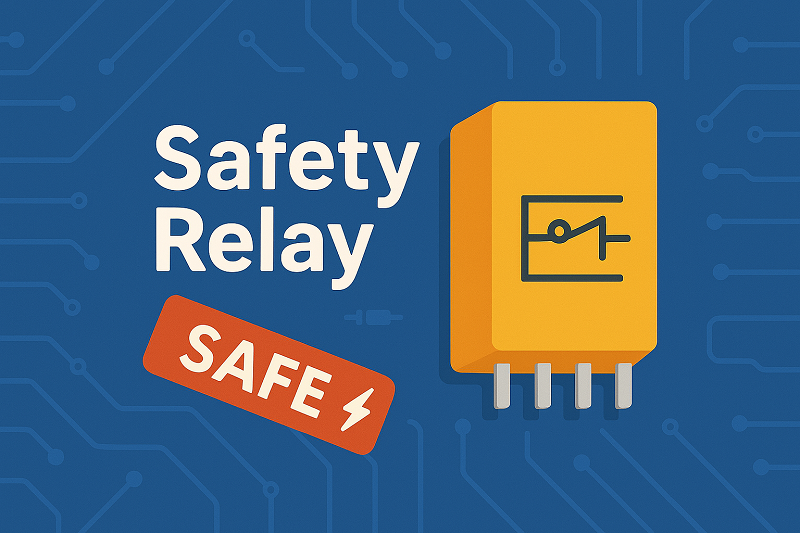 What is Safety Relay?
12 April 202525596
 Photonic Integrated Circuits: Overcoming Challenges in Silicon Photonics
26 August 20243044
 Using ESP32 to Make an IoT Weather Station
24 February 20237022
 Top Picks for Circuit Breakers This Year
10 July 20256648
 How 10k Resistor Color Code Stacks Up Against 220 and 100k
03 September 20254646
 A Selection of the Most Representative Charts——Artificial Intelligence Index Report
18 March 2022955
Intersil (Renesas Electronics America)
In Stock: 35
United States
China
Canada
Japan
Russia
Germany
United Kingdom
Singapore
Italy
Hong Kong(China)
Taiwan(China)
France
Korea
Mexico
Netherlands
Malaysia
Austria
Spain
Switzerland
Poland
Thailand
Vietnam
India
United Arab Emirates
Afghanistan
Åland Islands
Albania
Algeria
American Samoa
Andorra
Angola
Anguilla
Antigua & Barbuda
Argentina
Armenia
Aruba
Australia
Azerbaijan
Bahamas
Bahrain
Bangladesh
Barbados
Belarus
Belgium
Belize
Benin
Bermuda
Bhutan
Bolivia
Bonaire, Sint Eustatius and Saba
Bosnia & Herzegovina
Botswana
Brazil
British Indian Ocean Territory
British Virgin Islands
Brunei
Bulgaria
Burkina Faso
Burundi
Cabo Verde
Cambodia
Cameroon
Cayman Islands
Central African Republic
Chad
Chile
Christmas Island
Cocos (Keeling) Islands
Colombia
Comoros
Congo
Congo (DRC)
Cook Islands
Costa Rica
Côte d’Ivoire
Croatia
Cuba
Curaçao
Cyprus
Czechia
Denmark
Djibouti
Dominica
Dominican Republic
Ecuador
Egypt
El Salvador
Equatorial Guinea
Eritrea
Estonia
Eswatini
Ethiopia
Falkland Islands
Faroe Islands
Fiji
Finland
French Guiana
French Polynesia
Gabon
Gambia
Georgia
Ghana
Gibraltar
Greece
Greenland
Grenada
Guadeloupe
Guam
Guatemala
Guernsey
Guinea
Guinea-Bissau
Guyana
Haiti
Honduras
Hungary
Iceland
Indonesia
Iran
Iraq
Ireland
Isle of Man
Israel
Jamaica
Jersey
Jordan
Kazakhstan
Kenya
Kiribati
Kosovo
Kuwait
Kyrgyzstan
Laos
Latvia
Lebanon
Lesotho
Liberia
Libya
Liechtenstein
Lithuania
Luxembourg
Macao(China)
Madagascar
Malawi
Maldives
Mali
Malta
Marshall Islands
Martinique
Mauritania
Mauritius
Mayotte
Micronesia
Moldova
Monaco
Mongolia
Montenegro
Montserrat
Morocco
Mozambique
Myanmar
Namibia
Nauru
Nepal
New Caledonia
New Zealand
Nicaragua
Niger
Nigeria
Niue
Norfolk Island
North Korea
North Macedonia
Northern Mariana Islands
Norway
Oman
Pakistan
Palau
Palestinian Authority
Panama
Papua New Guinea
Paraguay
Peru
Philippines
Pitcairn Islands
Portugal
Puerto Rico
Qatar
Réunion
Romania
Rwanda
Samoa
San Marino
São Tomé & Príncipe
Saudi Arabia
Senegal
Serbia
Seychelles
Sierra Leone
Sint Maarten
Slovakia
Slovenia
Solomon Islands
Somalia
South Africa
South Sudan
Sri Lanka
St Helena, Ascension, Tristan da Cunha
St. Barthélemy
St. Kitts & Nevis
St. Lucia
St. Martin
St. Pierre & Miquelon
St. Vincent & Grenadines
Sudan
Suriname
Svalbard & Jan Mayen
Sweden
Syria
Tajikistan
Tanzania
Timor-Leste
Togo
Tokelau
Tonga
Trinidad & Tobago
Tunisia
Turkey
Turkmenistan
Turks & Caicos Islands
Tuvalu
U.S. Outlying Islands
U.S. Virgin Islands
Uganda
Ukraine
Uruguay
Uzbekistan
Vanuatu
Vatican City
Venezuela
Wallis & Futuna
Yemen
Zambia
Zimbabwe
![ISL55001IBZ-T7]() ISL55001IBZ-T7
ISL55001IBZ-T7Intersil (Renesas Electronics America)
![ISL28210FBZ]() ISL28210FBZ
ISL28210FBZIntersil (Renesas Electronics America)
![EL5175IS]() EL5175IS
EL5175ISIntersil (Renesas Electronics America)
![ISL28213FUZ-T7]() ISL28213FUZ-T7
ISL28213FUZ-T7Intersil (Renesas Electronics America)
![CA3130EZ]() CA3130EZ
CA3130EZIntersil (Renesas Electronics America)
![ISL28158FBZ]() ISL28158FBZ
ISL28158FBZIntersil (Renesas Electronics America)
![CA3140EZ]() CA3140EZ
CA3140EZIntersil (Renesas Electronics America)
![ISL55002IBZ-T7]() ISL55002IBZ-T7
ISL55002IBZ-T7Intersil (Renesas Electronics America)
![CA3140AEZ]() CA3140AEZ
CA3140AEZIntersil (Renesas Electronics America)


