
 Product
 Brand
Brand Articles
 Tools
Tools
Kintex-7 XC7K410T Series: An Evergreen Mainstream Solution in FPGA


1V V 2.54mm mm FPGAs Kintex®-7 Series 676-BBGA, FCBGA 1mm mm 676
Deep dive into AMD (Xilinx) Kintex-7 XC7K410T FPGA: key features, selection tips, design considerations, and alternatives. Includes XC7K410T-1FFG900C specs, orderable MPNs and official documentation pointers.
Product Introduction
Engineer’s Takeaway
Positioning: The XC7K410T sits at the upper tier of the Kintex-7 family, offering the highest DSP and Block RAM count in the series without stepping up to the more expensive Virtex-7 line. It is optimized for "Best Price/Performance/Watt" in the 28nm generation.
Why it matters: Despite being a mature 28nm product, it remains a dominant choice for legacy infrastructure (LTE radios) and medical imaging where the massive logic density (400k+ cells) and 12.5 Gbps transceivers provide sufficient bandwidth at a lower cost than newer UltraScale+ devices.
Market status: Mature / Active. Widely available but designers for brand new high-longevity projects might consider the Artix UltraScale+ or Kintex UltraScale+ for longer term manufacturing security, though the 7-series supply chain remains robust.
Lifecycle Check: ✅ Active / Mature.
The Kintex-7 XC7K410T is a high-density FPGA designed for high-performance applications requiring a balance of power efficiency and high-speed I/O throughput, built on a 28nm process.

Figure 1: Kintex-7 XC7K410T product photo, Kintex-7 XC7K410T product photo top view
1. Technical Architecture and Core Advantages
The XC7K410T utilizes AMD (Xilinx) 28nm High Performance Low Power (HPL) process architecture. This architecture was a pivotal shift, unifying the logic fabric across Artix, Kintex, and Virtex families to allow easier IP portability.
1.1 How It Works (High-level)
At its core, the XC7K410T is a programmable logic fabric surrounded by hardened IP blocks. It features 406,720 Logic Cells organized into Configurable Logic Blocks (CLBs) for implementing custom digital circuits. The device integrates 16 GTX Transceivers capable of up to 12.5 Gbps, enabling high-bandwidth protocols like PCIe Gen2 and 10G Ethernet without external PHYs for short reach. The Agile Mixed Signal (AMS) block provides on-die analog-to-digital monitoring of temperature and voltage rails.
Figure 2: Internal block diagram
1.2 Feature Matrix
| Feature | What it is | Why it matters (engineering value) |
|---|---|---|
| Logic Density | 406,720 Logic Cells | Sufficient density for complex DSP algorithms (FFT, filtering) or soft-core processors (MicroBlaze). |
| DSP Resources | 1,540 DSP Slices | High parallelism for signal processing in radar, medical imaging, and wireless radio heads. |
| Block RAM | 28,620 Kb Total | Large on-chip buffering capacity reduces the need for external memory access, lowering latency. |
| Connectivity | 16 GTX Transceivers (12.5 Gbps) | Enables native support for high-speed serialized standards like 10GbE, PCIe, and CPRI. |
| Integrated IP | PCIe Gen2 Hard Block | Saves logic resources and timing closure effort for standard PC interoperability. |
Data source: DS182
1.3 Deep Dive: Key Differentiators
The XC7K410T distinguishes itself by offering Virtex-class DSP density at a Kintex price point. With 1,540 DSP slices, it significantly outperforms lower-end Artix-7 devices, making it the preferred choice for arithmetic-heavy workloads like beamforming in medical ultrasound or LTE baseband processing. The inclusion of Agile Mixed Signal (AMS) allows self-monitoring of power rails, often eliminating the need for an external dedicated system monitor chip.
2. Naming / Variant Map and Selection Guide
2.1 Part Number Decoding
The part number typically follows the structure: XC7K410T-[SpeedGrade][Package][TempGrade].
- Speed Grade: -3 (Fastest), -2 (Mid), -1 (Slowest/Standard).
- Package: FFG900 (900-pin BGA), FFG676 (676-pin BGA).
- Temp Grade: C (Commercial, 0°C to 85°C), E (Extended, 0°C to 100°C), I (Industrial, -40°C to 100°C).
2.2 Core Variant Comparison
| Variant | Key differences | Typical values | Best for |
|---|---|---|---|
| XC7K410T-1FFG900C | Base Speed, Commercial Temp | Speed Grade -1, 0°C to 85°C | Cost-sensitive commercial applications (e.g., standard broadcast gear). |
| XC7K410T-2FFG900C | Mid Speed, Commercial Temp | Speed Grade -2, 0°C to 85°C | Balanced performance designs needing slightly better timing margins. |
| XC7K410T-1FFG676C | Base Speed, Lower Pin Count | Speed Grade -1, Fewer IOs | Designs where PCB space is constrained and full I/O count is not required. |
| XC7K410T-3FFG900E | High Speed, Extended Temp | Speed Grade -3, 0°C to 100°C | High-performance compute acceleration or hotter environments. |
2.3 Quick Selection Checklist
Is your design constrained by I/O count? If yes, choose FFG900 (more user I/O) over FFG676.
Do you need PCIe Gen2 x8 support? Ensure the selected package bonds out the necessary MGT lanes.
Is the environment controlled? If strictly office/server room, Commercial (C) is sufficient. If outdoor/rugged, look for Industrial (I) or Extended (E).
3. Key Specifications Explained
Rule: Only include precise numeric values if Tier-1 inputs provide them. Otherwise, write qualitatively.
3.1 Power / Voltage / Operating Range
The Kintex-7 family typically operates on a VCCINT (internal core voltage) around 1.0V (standard) or 0.9V (low power -L variants) [AI Added: Standard 7-series values]. - Core Voltage (VCCINT): Requires a highly stable, low-ripple supply due to high current transients during logic switching. - Transceiver Voltage (MGTAVCC/MGTAVTT): Dedicated rails are required for the GTX transceivers to minimize jitter. - Note: Always perform a Power Delivery Network (PDN) analysis using the Xilinx Power Estimator (XPE) specific to your logic utilization.
3.2 Performance / Efficiency / Noise / Accuracy
Transceiver Throughput: Supports line rates up to 12.5 Gbps.
Memory Interface (MIG): Capable of interfacing with DDR3/DDR3L. Speeds depend largely on the speed grade selected (-3 offers highest memory bandwidth).
Logic Capacity: 406,720 Logic cells provide immense parallel processing capability, far exceeding standard microcontroller capabilities.
3.3 Thermal and Protection Behavior
The XC7K410T is a high-performance device that can dissipate significant heat (often >10W-20W depending on utilization). - Cooling: Active cooling (heatsink + fan) or chassis conduction cooling is almost always required. - Monitoring: The internal system monitor (SYSMON) tracks die temperature and allows for thermal shutdown logic to be implemented in the fabric.
3.4 Fast Spec Table
| Parameter | Value / Range | Notes |
|---|---|---|
| Logic Cells | 406,720 | Density optimized for heavy compute. |
| DSP Slices | 1,540 | Dedicated 25x18 multipliers. |
| Block RAM | 28,620 Kb | Combined capacity of 36Kb blocks. |
| Transceivers | Up to 16 | GTX type (up to 12.5 Gbps). |
| PCIe Support | Gen2 | [AI Added] Integrated Hard Block. |
| Process Node | 28nm | TSMC HPL process. |
For full electrical characteristics, refer to Official Datasheet DS182.
4. Design Notes and Common Integration Issues
4.1 Reference Design Notes
Designing with the XC7K410T requires strict attention to PCB layout, particularly for the high-speed serial links. - Layer Stack: A minimum of 10-12 layers is typically recommended to route the FFG900 BGA escape and manage power planes. - Decoupling: Place capacitors as close as possible to the BGA balls on the bottom side of the PCB to minimize inductance for VCCINT.
📺 Video: Kintex-7 XC7K410T design guide or tutorial
4.2 Layout / EMI / Thermal Checklist
[ ] MGT Routing: Route GTX lanes as differential pairs with loose coupling to avoid crosstalk. Match lengths precisely.
[ ] Clocking: Use dedicated clock input pins (MRCC/SRCC) for global clocks. Do not route clocks on standard I/O pins.
[ ] Thermal Relief: Ensure the thermal solution (heatsink) has appropriate mounting pressure; avoid warping the large BGA package.
4.3 Common Mistakes (Quick Debug)
| Context / Scenario | Symptom | Fix / Workaround |
|---|---|---|
| Configuration | FPGA fails to boot / DONE pin remains low | Check Mode pins (M0-M2) settings and ensure the configuration PROM voltage matches the bank voltage (3.3V vs 1.8V). [AI Added: Common 7-series pitfall] |
| PCIe Link | Link training failure | Verify reference clock quality (typically 100MHz HCSL) and ensure MGTREFCLK pins are correctly assigned. [AI Added: Standard PCIe debug] |
| Power Up | Excessive inrush current | Ensure power rails sequence strictly according to datasheet (typically VCCINT -> VCCBRAM -> VCCAUX -> VCCO). |
5. Typical Applications
Application Reasoning
The XC7K410T is chosen specifically where the DSP-to-Logic ratio is high.
- Wireless Infrastructure: Suitable due to 1,540 DSP Slices handling Digital Front End (DFE) algorithms like Digital Pre-Distortion (DPD) for LTE/5G radios.
- Medical Imaging: Leverages the 28Mb Block RAM to buffer high-resolution image data from ultrasound probes before processing.
- High-End Wired Comms: Uses 16 GTX Transceivers to aggregate multiple 10G Ethernet links in backplane acceleration.
5.1 Wireless Infrastructure (LTE/5G)
In Remote Radio Heads (RRH), the XC7K410T processes IQ data. The high-speed GTX transceivers handle the CPRI/OBSAI interface to the baseband unit, while the DSP slices perform filtering and up/down-conversion.
5.2 Medical Imaging (Ultrasound/CT)
The device is used in the beamforming stage. The massive I/O count of the FFG900 package allows connection to high-channel-count ADC arrays. The logic fabric performs delay-and-sum beamforming in real-time.
5.3 Broadcast Video
Supports 4K/8K video processing pipelines. The integrated PCIe block allows the FPGA to sit on a capture card, streaming raw video data to a host PC, while the logic fabric handles color space conversion or encoding.
6. Competitors and Alternatives
6.1 Comparison Matrix
| Dimension | Kintex-7 XC7K410T | Intel Arria 10 (GX) | Microchip PolarFire |
|---|---|---|---|
| Primary Advantage | Mature Ecosystem, Best-in-class DSP/Price | Higher floating-point performance (Hard floating point DSP) | Lowest static power, instant-on, SEU immunity |
| Technology | 28nm HPL | 20nm | 28nm Non-volatile |
| Transceivers | 12.5 Gbps | Up to ~17 Gbps - 28 Gbps [AI Added: Qualitative] | 12.7 Gbps |
| Hard IP | PCIe Gen2 | PCIe Gen3, Hard Memory Controllers [AI Added] | PCIe Gen2, Security |
6.2 Alternative Paths
✅ Pin-to-pin alternatives: Users can often migrate within the Kintex-7 family (e.g., XC7K325T) if the simpler footprint (FFG676/900) matches, though the XC7K410T is often the top of the specific footprint density.
🟡 Functional alternatives (Redesign required): Kintex UltraScale (20nm) offers significant power savings and PCIe Gen3 but necessitates a PCB redesign due to different voltage rails and package pinouts.
🔴 Not recommended: Using Artix-7 for these applications; Artix-7 generally lacks the sheer number of GTX transceivers and DSP slices required for XC7K410T-class workloads.
7. FAQ
Q1: What is the main difference between Kintex-7 and Virtex-7?
A: Kintex-7 is optimized for the best price/performance ratio, whereas Virtex-7 is optimized for maximum system capacity and performance. Virtex-7 devices typically feature significantly higher logic counts, faster transceivers (GTH/GTZ), and higher bandwidth memory interfaces, but at a higher cost and power consumption.Q2: Does the XC7K410T support PCIe Gen3?
A: The XC7K410T includes a hardened integrated block for **PCIe Gen2**. While the GTX transceivers can theoretically run at speeds supporting Gen3 (8.0 GT/s), the hardened endpoint block is Gen2. Implementing Gen3 usually requires soft-core IP or moving to the Kintex UltraScale series.Q3: Can I run this device without a heat sink?
A: [AI Added] Highly unlikely for typical designs. The static power of such a large device, combined with dynamic power from 400k logic cells and high-speed transceivers, usually demands a robust thermal solution (heatsink with airflow) to keep the junction temperature below the 85°C (Commercial) or 100°C (Extended/Industrial) limit.Q4: What software is required to design for the XC7K410T?
A: The XC7K410T is fully supported by the **AMD (Xilinx) Vivado Design Suite**, starting from version 2012.x onwards. It is not supported by the legacy ISE Design Suite (which generally stopped at Virtex-6/Spartan-6, though some early 7-series support existed, Vivado is the standard).8. Orderable MPN List
Prices and real-time inventory change frequently. Do not fabricate.
| MPN | Description | Status |
|---|---|---|
| XC7K410T-1FFG900C | 410K Logic Cells, Speed -1, Commercial, 900-pin BGA | 🟢 In Stock (Typically) |
| XC7K410T-2FFG900C | 410K Logic Cells, Speed -2, Commercial, 900-pin BGA | 🟢 In Stock (Typically) |
| XC7K410T-1FFG676C | 410K Logic Cells, Speed -1, Commercial, 676-pin BGA | 🟡 Limited / Check Stock |
| XC7K410T-3FFG900E | 410K Logic Cells, Speed -3, Extended, 900-pin BGA | 🟡 Limited / Check Stock |
Legend: - 🟢 In Stock - 🟡 Limited - 🔴 Obsolete
9. Resources and Downloads
9.1 Official Documents
| Document | ID / Name | Notes |
|---|---|---|
| Datasheet | DS182: Kintex-7 FPGAs Data Sheet: DC and AC Switching Characteristics | Primary source for electrical limits and timing. |
| Overview | 7 Series FPGAs Overview | High-level architecture and feature summary. |
| Packaging | UG475: 7 Series FPGAs Packaging and Pinout | Essential for PCB footprint creation. |
9.2 Tools / Software
Vivado Design Suite: The primary IDE for synthesis, implementation, and bitstream generation.
Xilinx Power Estimator (XPE): Spreadsheet tool for estimating power consumption before design completion.
9.3 Support
AMD Xilinx Support Community: Official forums for technical troubleshooting.
Service Requests: Available for direct customer support on complex issues.
Disclaimer
This article is for selection and design reference only. Always verify final specifications and electrical limits against the latest official AMD (Xilinx) documentation.
Specifications
- TypeParameter
- Factory Lead Time12 Weeks
- Mount
In electronic components, the term "Mount" typically refers to the method or process of physically attaching or fixing a component onto a circuit board or other electronic device. This can involve soldering, adhesive bonding, or other techniques to secure the component in place. The mounting process is crucial for ensuring proper electrical connections and mechanical stability within the electronic system. Different components may have specific mounting requirements based on their size, shape, and function, and manufacturers provide guidelines for proper mounting procedures to ensure optimal performance and reliability of the electronic device.
Surface Mount - Mounting Type
The "Mounting Type" in electronic components refers to the method used to attach or connect a component to a circuit board or other substrate, such as through-hole, surface-mount, or panel mount.
Surface Mount - Package / Case
refers to the protective housing that encases an electronic component, providing mechanical support, electrical connections, and thermal management.
676-BBGA, FCBGA - Number of Pins676
- Number of I/Os400
- Operating Temperature
The operating temperature is the range of ambient temperature within which a power supply, or any other electrical equipment, operate in. This ranges from a minimum operating temperature, to a peak or maximum operating temperature, outside which, the power supply may fail.
0°C~100°C TJ - Packaging
Semiconductor package is a carrier / shell used to contain and cover one or more semiconductor components or integrated circuits. The material of the shell can be metal, plastic, glass or ceramic.
Tray - Series
In electronic components, the "Series" refers to a group of products that share similar characteristics, designs, or functionalities, often produced by the same manufacturer. These components within a series typically have common specifications but may vary in terms of voltage, power, or packaging to meet different application needs. The series name helps identify and differentiate between various product lines within a manufacturer's catalog.
Kintex®-7 - Published2009
- JESD-609 Code
The "JESD-609 Code" in electronic components refers to a standardized marking code that indicates the lead-free solder composition and finish of electronic components for compliance with environmental regulations.
e1 - Pbfree Code
The "Pbfree Code" parameter in electronic components refers to the code or marking used to indicate that the component is lead-free. Lead (Pb) is a toxic substance that has been widely used in electronic components for many years, but due to environmental concerns, there has been a shift towards lead-free alternatives. The Pbfree Code helps manufacturers and users easily identify components that do not contain lead, ensuring compliance with regulations and promoting environmentally friendly practices. It is important to pay attention to the Pbfree Code when selecting electronic components to ensure they meet the necessary requirements for lead-free applications.
yes - Part Status
Parts can have many statuses as they progress through the configuration, analysis, review, and approval stages.
Active - Moisture Sensitivity Level (MSL)
Moisture Sensitivity Level (MSL) is a standardized rating that indicates the susceptibility of electronic components, particularly semiconductors, to moisture-induced damage during storage and the soldering process, defining the allowable exposure time to ambient conditions before they require special handling or baking to prevent failures
4 (72 Hours) - Number of Terminations676
- ECCN Code
An ECCN (Export Control Classification Number) is an alphanumeric code used by the U.S. Bureau of Industry and Security to identify and categorize electronic components and other dual-use items that may require an export license based on their technical characteristics and potential for military use.
3A991.D - Terminal Finish
Terminal Finish refers to the surface treatment applied to the terminals or leads of electronic components to enhance their performance and longevity. It can improve solderability, corrosion resistance, and overall reliability of the connection in electronic assemblies. Common finishes include nickel, gold, and tin, each possessing distinct properties suitable for various applications. The choice of terminal finish can significantly impact the durability and effectiveness of electronic devices.
Tin/Silver/Copper (Sn96.5Ag3.0Cu0.5) - HTS Code
HTS (Harmonized Tariff Schedule) codes are product classification codes between 8-1 digits. The first six digits are an HS code, and the countries of import assign the subsequent digits to provide additional classification. U.S. HTS codes are 1 digits and are administered by the U.S. International Trade Commission.
8542.39.00.01 - Voltage - Supply
Voltage - Supply refers to the range of voltage levels that an electronic component or circuit is designed to operate with. It indicates the minimum and maximum supply voltage that can be applied for the device to function properly. Providing supply voltages outside this range can lead to malfunction, damage, or reduced performance. This parameter is critical for ensuring compatibility between different components in a circuit.
0.97V~1.03V - Terminal Position
In electronic components, the term "Terminal Position" refers to the physical location of the connection points on the component where external electrical connections can be made. These connection points, known as terminals, are typically used to attach wires, leads, or other components to the main body of the electronic component. The terminal position is important for ensuring proper connectivity and functionality of the component within a circuit. It is often specified in technical datasheets or component specifications to help designers and engineers understand how to properly integrate the component into their circuit designs.
BOTTOM - Terminal Form
Occurring at or forming the end of a series, succession, or the like; closing; concluding.
BALL - Peak Reflow Temperature (Cel)
Peak Reflow Temperature (Cel) is a parameter that specifies the maximum temperature at which an electronic component can be exposed during the reflow soldering process. Reflow soldering is a common method used to attach electronic components to a circuit board. The Peak Reflow Temperature is crucial because it ensures that the component is not damaged or degraded during the soldering process. Exceeding the specified Peak Reflow Temperature can lead to issues such as component failure, reduced performance, or even permanent damage to the component. It is important for manufacturers and assemblers to adhere to the recommended Peak Reflow Temperature to ensure the reliability and functionality of the electronic components.
NOT SPECIFIED - Supply Voltage
Supply voltage refers to the electrical potential difference provided to an electronic component or circuit. It is crucial for the proper operation of devices, as it powers their functions and determines performance characteristics. The supply voltage must be within specified limits to ensure reliability and prevent damage to components. Different electronic devices have specific supply voltage requirements, which can vary widely depending on their design and intended application.
0.9V - Terminal Pitch
The center distance from one pole to the next.
1mm - Time@Peak Reflow Temperature-Max (s)
Time@Peak Reflow Temperature-Max (s) refers to the maximum duration that an electronic component can be exposed to the peak reflow temperature during the soldering process, which is crucial for ensuring reliable solder joint formation without damaging the component.
NOT SPECIFIED - Base Part Number
The "Base Part Number" (BPN) in electronic components serves a similar purpose to the "Base Product Number." It refers to the primary identifier for a component that captures the essential characteristics shared by a group of similar components. The BPN provides a fundamental way to reference a family or series of components without specifying all the variations and specific details.
XC7K410T - Pin Count
a count of all of the component leads (or pins)
676 - Number of Outputs400
- Qualification Status
An indicator of formal certification of qualifications.
Not Qualified - Operating Supply Voltage
The voltage level by which an electrical system is designated and to which certain operating characteristics of the system are related.
1V - Power Supplies
an electronic circuit that converts the voltage of an alternating current (AC) into a direct current (DC) voltage.?
0.91.83.3V - RAM Size
RAM size refers to the amount of random access memory (RAM) available in an electronic component, such as a computer or smartphone. RAM is a type of volatile memory that stores data and instructions that are actively being used by the device's processor. The RAM size is typically measured in gigabytes (GB) and determines how much data the device can store and access quickly for processing. A larger RAM size allows for smoother multitasking, faster loading times, and better overall performance of the electronic component. It is an important factor to consider when choosing a device, especially for tasks that require a lot of memory, such as gaming, video editing, or running multiple applications simultaneously.
3.5MB - Programmable Logic Type
Generally, programmable logic devices can be described as being one of three different types: Simple programmable logic devices (SPLD) Complex programmable logic devices (CPLD) Field programmable logic devices (FPGA).
FIELD PROGRAMMABLE GATE ARRAY - Number of Logic Elements/Cells406720
- Total RAM Bits
Total RAM Bits refers to the total number of memory bits that can be stored in a Random Access Memory (RAM) component. RAM is a type of computer memory that allows data to be accessed in any random order, making it faster than other types of memory like hard drives. The total RAM bits indicate the capacity of the RAM chip to store data temporarily for quick access by the computer's processor. The more total RAM bits a component has, the more data it can store and process at any given time, leading to improved performance and multitasking capabilities.
29306880 - Number of LABs/CLBs31775
- Number of Registers508400
- Combinatorial Delay of a CLB-Max
The Combinatorial Delay of a CLB-Max in electronic components refers to the time it takes for a signal to propagate through a combinational logic block (CLB) within a Field-Programmable Gate Array (FPGA) to reach its output. This delay is influenced by factors such as the complexity of the logic function being implemented, the routing resources available, and the physical distance the signal needs to travel within the CLB. Understanding and optimizing the Combinatorial Delay of a CLB-Max is crucial in designing efficient and high-performance digital circuits, as it directly impacts the overall speed and functionality of the FPGA design. By minimizing this delay, designers can achieve faster operation and improved performance in their electronic systems.
0.91 ns - Length27mm
- Height Seated (Max)
Height Seated (Max) is a parameter in electronic components that refers to the maximum allowable height of the component when it is properly seated or installed on a circuit board or within an enclosure. This specification is crucial for ensuring proper fit and alignment within the overall system design. Exceeding the maximum seated height can lead to mechanical interference, electrical shorts, or other issues that may impact the performance and reliability of the electronic device. Manufacturers provide this information to help designers and engineers select components that will fit within the designated space and function correctly in the intended application.
2.54mm - Width27mm
- RoHS Status
RoHS means “Restriction of Certain Hazardous Substances” in the “Hazardous Substances Directive” in electrical and electronic equipment.
ROHS3 Compliant
Parts with Similar Specs
- ImagePart NumberManufacturerPackage / CaseNumber of PinsNumber of Logic Elements/CellsNumber of I/ORAM SizeSupply VoltagePublishedTerminal PitchView Compare
![XC7K410T-L2FBG676E]()
XC7K410T-L2FBG676E
676-BBGA, FCBGA
676
406720
400
3.5 MB
0.9 V
2009
1 mm
![XC7K325T-1FBG676I]()
676-BBGA, FCBGA
676
326080
400
2 MB
1 V
2009
1 mm
![XC7K325T-1FBG676C]()
676-BBGA, FCBGA
676
326080
400
2 MB
1 V
2009
1 mm
![XC7K325T-2FBG676I]()
676-BBGA, FCBGA
676
326080
400
2 MB
1 V
2009
1 mm

Datasheet PDF
- Datasheets :
- PCN Design/Specification :
- PCN Assembly/Origin :
- PCN Packaging :
- Environmental Information :
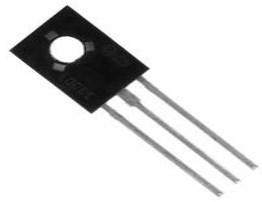
 TIP29C Transistor: Where & How to Use?
11 November 20212791
 TPS1H000AQDGNRQ1 High-Side Switch: Circuit, Pinout, and Datasheet
31 March 2022586
 What is BD139?
04 August 20215987
![TDA7056B Audio Amplifiers: Schematic, Pinout, and Datasheet [Video&FAQ]](https://res.utmel.com/Images/Article/0a597bc3-db55-444b-b6f4-38bd051b7609.png) TDA7056B Audio Amplifiers: Schematic, Pinout, and Datasheet [Video&FAQ]
TDA7056B Audio Amplifiers: Schematic, Pinout, and Datasheet [Video&FAQ]06 January 202214271
 Buying the LTM8064? Read This First — Specs, Thermal Traps, and Cheaper Alternatives
23 March 2026228
 TS5V330D Video Switch: Pinout, Features and Specification
14 August 2024968
 TDA2822M Low-Voltage Power Amplifier: Datasheet, Pinout and Circuit
20 October 202172969
 Yageo CC0805KRX7R9BB104 Alternatives for Engineers
29 August 2025861
 The Comprehensive Guide to MOSFETs: Principles, Types, and Parameters (2026 Edition)
16 January 202620179
 Basic Introduction to Power Amplifier
09 January 202610668
 NPN Transistors and PNP Transistors
29 October 20209837
 How to Design an Accurate DC Power Supply
15 October 20255527
 Opportunities and Challenges for 2D Materials
22 March 20225801
 Cellular IoT Transmit Module for Enhanced Connectivity and Power Efficiency with Extended Battery Life
30 January 20242267
 Top 5 SR44 Battery Brands for Reliable Power
20 August 20254902
 What is RF Switch?
16 November 20217679
Xilinx Inc.
In Stock
United States
China
Canada
Japan
Russia
Germany
United Kingdom
Singapore
Italy
Hong Kong(China)
Taiwan(China)
France
Korea
Mexico
Netherlands
Malaysia
Austria
Spain
Switzerland
Poland
Thailand
Vietnam
India
United Arab Emirates
Afghanistan
Åland Islands
Albania
Algeria
American Samoa
Andorra
Angola
Anguilla
Antigua & Barbuda
Argentina
Armenia
Aruba
Australia
Azerbaijan
Bahamas
Bahrain
Bangladesh
Barbados
Belarus
Belgium
Belize
Benin
Bermuda
Bhutan
Bolivia
Bonaire, Sint Eustatius and Saba
Bosnia & Herzegovina
Botswana
Brazil
British Indian Ocean Territory
British Virgin Islands
Brunei
Bulgaria
Burkina Faso
Burundi
Cabo Verde
Cambodia
Cameroon
Cayman Islands
Central African Republic
Chad
Chile
Christmas Island
Cocos (Keeling) Islands
Colombia
Comoros
Congo
Congo (DRC)
Cook Islands
Costa Rica
Côte d’Ivoire
Croatia
Cuba
Curaçao
Cyprus
Czechia
Denmark
Djibouti
Dominica
Dominican Republic
Ecuador
Egypt
El Salvador
Equatorial Guinea
Eritrea
Estonia
Eswatini
Ethiopia
Falkland Islands
Faroe Islands
Fiji
Finland
French Guiana
French Polynesia
Gabon
Gambia
Georgia
Ghana
Gibraltar
Greece
Greenland
Grenada
Guadeloupe
Guam
Guatemala
Guernsey
Guinea
Guinea-Bissau
Guyana
Haiti
Honduras
Hungary
Iceland
Indonesia
Iran
Iraq
Ireland
Isle of Man
Israel
Jamaica
Jersey
Jordan
Kazakhstan
Kenya
Kiribati
Kosovo
Kuwait
Kyrgyzstan
Laos
Latvia
Lebanon
Lesotho
Liberia
Libya
Liechtenstein
Lithuania
Luxembourg
Macao(China)
Madagascar
Malawi
Maldives
Mali
Malta
Marshall Islands
Martinique
Mauritania
Mauritius
Mayotte
Micronesia
Moldova
Monaco
Mongolia
Montenegro
Montserrat
Morocco
Mozambique
Myanmar
Namibia
Nauru
Nepal
New Caledonia
New Zealand
Nicaragua
Niger
Nigeria
Niue
Norfolk Island
North Korea
North Macedonia
Northern Mariana Islands
Norway
Oman
Pakistan
Palau
Palestinian Authority
Panama
Papua New Guinea
Paraguay
Peru
Philippines
Pitcairn Islands
Portugal
Puerto Rico
Qatar
Réunion
Romania
Rwanda
Samoa
San Marino
São Tomé & Príncipe
Saudi Arabia
Senegal
Serbia
Seychelles
Sierra Leone
Sint Maarten
Slovakia
Slovenia
Solomon Islands
Somalia
South Africa
South Sudan
Sri Lanka
St Helena, Ascension, Tristan da Cunha
St. Barthélemy
St. Kitts & Nevis
St. Lucia
St. Martin
St. Pierre & Miquelon
St. Vincent & Grenadines
Sudan
Suriname
Svalbard & Jan Mayen
Sweden
Syria
Tajikistan
Tanzania
Timor-Leste
Togo
Tokelau
Tonga
Trinidad & Tobago
Tunisia
Turkey
Turkmenistan
Turks & Caicos Islands
Tuvalu
U.S. Outlying Islands
U.S. Virgin Islands
Uganda
Ukraine
Uruguay
Uzbekistan
Vanuatu
Vatican City
Venezuela
Wallis & Futuna
Yemen
Zambia
Zimbabwe
![XC6SLX45-2FGG484C]() XC6SLX45-2FGG484C
XC6SLX45-2FGG484CXilinx Inc.
![XC3S400-4PQG208I]() XC3S400-4PQG208I
XC3S400-4PQG208IXilinx Inc.
![XC6SLX9-2CSG225I]() XC6SLX9-2CSG225I
XC6SLX9-2CSG225IXilinx Inc.
![XCV1000-4BG560C]() XCV1000-4BG560C
XCV1000-4BG560CXilinx Inc.
![XC5VFX130T-2FFG1738I]() XC5VFX130T-2FFG1738I
XC5VFX130T-2FFG1738IXilinx Inc.
![XCV50E-7FG256I]() XCV50E-7FG256I
XCV50E-7FG256IXilinx Inc.
![XC2S400E-6FGG456C]() XC2S400E-6FGG456C
XC2S400E-6FGG456CXilinx Inc.
![XC2S100E-6FT256C]() XC2S100E-6FT256C
XC2S100E-6FT256CXilinx Inc.
![XC2S15-5CS144C]() XC2S15-5CS144C
XC2S15-5CS144CXilinx Inc.
![XCS10-3VQG100C]() XCS10-3VQG100C
XCS10-3VQG100CXilinx Inc.


