
 Product
 Brand
Brand Articles
 Tools
Tools
RT9193 Ultra-Fast CMOS LDO Regulator: Datasheet pdf, Ultra-Fast Regulator and Specifications


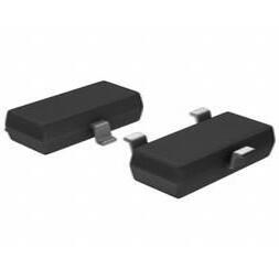
Enable Fixed 0.939mm PMIC SC-74A, SOT-753
The RT9193 is designed for portable RF and wireless applications with demanding performance and space requirements. This article is going to explain datasheet pdf, pinout, specifications, and other details about the RT9193 Ultra-Fast regulator. Furthermore, there is a huge range of semiconductors, capacitors, resistors, and ICs in stock. Welcome your RFQ!
RT9193 Pinout

RT9193 Pinout
| Pin No. | Pin Name | Description |
| 1 | Vin | Power Input Voltage |
| 2 | GND | Ground |
| 3 | EN | Chip Enable (Active High). This pin is a high impedance. Connect a pull low 100kΩ Resistor to GND when the control signal is floating. |
| 4 | BP | Reference Noise Bypass. For the lowest noise performance, connect a 22nF Capacitor between the BP and GND pins. |
| 5 | Vout | Output Voltage |
What is RT9193?
The RT9193 is a low-noise, Ultra-Fast CMOS LDO regulator with a shutdown power consumption of less than 0.01A and a rapid turn-on time of less than 50s. The RT9193 offers a low dropout voltage of 220 mV at 300 mA, a wide operating voltage range of 2.5V to 5.5V, and an output voltage of 1.5V to 5V.
RT9193 CAD Model

RT9193 Symbol

RT9193 Footprint

RT9193 3D Model
Specifications
- TypeParameter
- Factory Lead Time18 Weeks
- Mount
In electronic components, the term "Mount" typically refers to the method or process of physically attaching or fixing a component onto a circuit board or other electronic device. This can involve soldering, adhesive bonding, or other techniques to secure the component in place. The mounting process is crucial for ensuring proper electrical connections and mechanical stability within the electronic system. Different components may have specific mounting requirements based on their size, shape, and function, and manufacturers provide guidelines for proper mounting procedures to ensure optimal performance and reliability of the electronic device.
Surface Mount - Mounting Type
The "Mounting Type" in electronic components refers to the method used to attach or connect a component to a circuit board or other substrate, such as through-hole, surface-mount, or panel mount.
Surface Mount - Package / Case
refers to the protective housing that encases an electronic component, providing mechanical support, electrical connections, and thermal management.
SC-74A, SOT-753 - Number of Pins5
- Operating Temperature
The operating temperature is the range of ambient temperature within which a power supply, or any other electrical equipment, operate in. This ranges from a minimum operating temperature, to a peak or maximum operating temperature, outside which, the power supply may fail.
-40°C~125°C - Packaging
Semiconductor package is a carrier / shell used to contain and cover one or more semiconductor components or integrated circuits. The material of the shell can be metal, plastic, glass or ceramic.
Tape & Reel (TR) - Published2013
- Part Status
Parts can have many statuses as they progress through the configuration, analysis, review, and approval stages.
Active - Moisture Sensitivity Level (MSL)
Moisture Sensitivity Level (MSL) is a standardized rating that indicates the susceptibility of electronic components, particularly semiconductors, to moisture-induced damage during storage and the soldering process, defining the allowable exposure time to ambient conditions before they require special handling or baking to prevent failures
3 (168 Hours) - Number of Terminations5
- ECCN Code
An ECCN (Export Control Classification Number) is an alphanumeric code used by the U.S. Bureau of Industry and Security to identify and categorize electronic components and other dual-use items that may require an export license based on their technical characteristics and potential for military use.
EAR99 - Terminal Position
In electronic components, the term "Terminal Position" refers to the physical location of the connection points on the component where external electrical connections can be made. These connection points, known as terminals, are typically used to attach wires, leads, or other components to the main body of the electronic component. The terminal position is important for ensuring proper connectivity and functionality of the component within a circuit. It is often specified in technical datasheets or component specifications to help designers and engineers understand how to properly integrate the component into their circuit designs.
DUAL - Terminal Form
Occurring at or forming the end of a series, succession, or the like; closing; concluding.
GULL WING - Peak Reflow Temperature (Cel)
Peak Reflow Temperature (Cel) is a parameter that specifies the maximum temperature at which an electronic component can be exposed during the reflow soldering process. Reflow soldering is a common method used to attach electronic components to a circuit board. The Peak Reflow Temperature is crucial because it ensures that the component is not damaged or degraded during the soldering process. Exceeding the specified Peak Reflow Temperature can lead to issues such as component failure, reduced performance, or even permanent damage to the component. It is important for manufacturers and assemblers to adhere to the recommended Peak Reflow Temperature to ensure the reliability and functionality of the electronic components.
NOT SPECIFIED - Number of Functions1
- Terminal Pitch
The center distance from one pole to the next.
0.939mm - Time@Peak Reflow Temperature-Max (s)
Time@Peak Reflow Temperature-Max (s) refers to the maximum duration that an electronic component can be exposed to the peak reflow temperature during the soldering process, which is crucial for ensuring reliable solder joint formation without damaging the component.
NOT SPECIFIED - Voltage - Input (Max)
Voltage - Input (Max) is a parameter in electronic components that specifies the maximum voltage that can be safely applied to the input of the component without causing damage. This parameter is crucial for ensuring the proper functioning and longevity of the component. Exceeding the maximum input voltage can lead to electrical overstress, which may result in permanent damage or failure of the component. It is important to carefully adhere to the specified maximum input voltage to prevent any potential issues and maintain the reliability of the electronic system.
5.5V - Output Voltage
Output voltage is a crucial parameter in electronic components that refers to the voltage level produced by the component as a result of its operation. It represents the electrical potential difference between the output terminal of the component and a reference point, typically ground. The output voltage is a key factor in determining the performance and functionality of the component, as it dictates the level of voltage that will be delivered to the connected circuit or load. It is often specified in datasheets and technical specifications to ensure compatibility and proper functioning within a given system.
1.5V - Output Type
The "Output Type" parameter in electronic components refers to the type of signal or data that is produced by the component as an output. This parameter specifies the nature of the output signal, such as analog or digital, and can also include details about the voltage levels, current levels, frequency, and other characteristics of the output signal. Understanding the output type of a component is crucial for ensuring compatibility with other components in a circuit or system, as well as for determining how the output signal can be utilized or processed further. In summary, the output type parameter provides essential information about the nature of the signal that is generated by the electronic component as its output.
Fixed - Output Configuration
Output Configuration in electronic components refers to the arrangement or setup of the output pins or terminals of a device. It defines how the output signals are structured and how they interact with external circuits or devices. The output configuration can determine the functionality and compatibility of the component in a circuit design. Common types of output configurations include single-ended, differential, open-drain, and push-pull configurations, each serving different purposes and applications in electronic systems. Understanding the output configuration of a component is crucial for proper integration and operation within a circuit.
Positive - Control Features
Control features in electronic components refer to specific functionalities or characteristics that allow users to manage and regulate the operation of the component. These features are designed to provide users with control over various aspects of the component's performance, such as adjusting settings, monitoring parameters, or enabling specific modes of operation. Control features can include options for input/output configurations, power management, communication protocols, and other settings that help users customize and optimize the component's behavior according to their requirements. Overall, control features play a crucial role in enhancing the flexibility, usability, and performance of electronic components in various applications.
Enable - Output Voltage 1
Output Voltage 1 is a parameter commonly found in electronic components such as voltage regulators, power supplies, and amplifiers. It refers to the voltage level that is produced or delivered by the component at a specific output terminal or pin. This parameter is crucial for determining the performance and functionality of the component in a circuit. The specified output voltage should meet the requirements of the connected devices or components to ensure proper operation and compatibility. It is important to carefully consider and verify the output voltage 1 specification when selecting and using electronic components in a design or application.
1.5V - Number of Regulators
A regulator is a mechanism or device that controls something such as pressure, temperature, or fluid flow. The voltage regulator keeps the power level stabilized. A regulator is a mechanism or device that controls something such as pressure, temperature, or fluid flow.
1 - Min Input Voltage
The parameter "Min Input Voltage" in electronic components refers to the minimum voltage level that must be applied to the component for it to operate within its specified parameters. This value is crucial as providing a voltage below this minimum threshold may result in the component malfunctioning or not functioning at all. It is important to adhere to the specified minimum input voltage to ensure the proper operation and longevity of the electronic component. Failure to meet this requirement may lead to potential damage to the component or the overall system in which it is used.
2.5V - Protection Features
Protection features in electronic components refer to the built-in mechanisms or functionalities designed to safeguard the component and the overall system from various external factors or internal faults. These features are crucial for ensuring the reliability, longevity, and safety of the electronic device. Common protection features include overvoltage protection, overcurrent protection, reverse polarity protection, thermal protection, and short-circuit protection. By activating these features when necessary, the electronic component can prevent damage, malfunctions, or hazards that may arise from abnormal operating conditions or unforeseen events. Overall, protection features play a vital role in enhancing the robustness and resilience of electronic components in diverse applications.
Over Current, Over Temperature - Current - Quiescent (Iq)
The parameter "Current - Quiescent (Iq)" in electronic components refers to the amount of current consumed by a device when it is in a quiescent or idle state, meaning when it is not actively performing any tasks or operations. This parameter is important because it represents the baseline power consumption of the device even when it is not actively being used. A lower quiescent current (Iq) value is desirable as it indicates that the device is more energy-efficient and will consume less power when not in use, which can help extend battery life in portable devices and reduce overall power consumption in electronic systems. Designers often pay close attention to the quiescent current specification when selecting components for low-power applications or battery-operated devices.
130μA - PSRR
PSRR stands for Power Supply Rejection Ratio. It is a measure of how well a device, such as an amplifier or a voltage regulator, can reject variations in the power supply voltage. A high PSRR value indicates that the device is able to maintain its performance even when the power supply voltage fluctuates. This parameter is important in ensuring stable and reliable operation of electronic components, especially in applications where the power supply voltage may not be perfectly regulated. A good PSRR helps to minimize noise and interference in the output signal of the device.
70dB ~ 50dB (100Hz ~ 10kHz) - Min Current Limit
Min Current Limit is a parameter in electronic components that refers to the minimum amount of current that must flow through the component to ensure proper operation. This parameter is important because if the current falls below this limit, the component may not function as intended or may even be damaged. Manufacturers specify the minimum current limit to help users understand the operating conditions and limitations of the component. It is crucial to ensure that the current flowing through the component remains above the specified minimum limit to maintain its performance and reliability.
360mA - Nominal Output Voltage
Nominal Output Voltage refers to the specified or intended voltage level that an electronic component or device is designed to provide as output under normal operating conditions. It is a crucial parameter that indicates the expected voltage level that the component will deliver to the connected circuit or load. This value is typically specified by the manufacturer and is important for ensuring proper functionality and compatibility within a system. It is important to note that the actual output voltage may vary slightly due to factors such as load variations, temperature changes, and other environmental conditions.
1.5V - REACH SVHC
The parameter "REACH SVHC" in electronic components refers to the compliance with the Registration, Evaluation, Authorization, and Restriction of Chemicals (REACH) regulation regarding Substances of Very High Concern (SVHC). SVHCs are substances that may have serious effects on human health or the environment, and their use is regulated under REACH to ensure their safe handling and minimize their impact.Manufacturers of electronic components need to declare if their products contain any SVHCs above a certain threshold concentration and provide information on the safe use of these substances. This information allows customers to make informed decisions about the potential risks associated with using the components and take appropriate measures to mitigate any hazards.Ensuring compliance with REACH SVHC requirements is essential for electronics manufacturers to meet regulatory standards, protect human health and the environment, and maintain transparency in their supply chain. It also demonstrates a commitment to sustainability and responsible manufacturing practices in the electronics industry.
No SVHC - RoHS Status
RoHS means “Restriction of Certain Hazardous Substances” in the “Hazardous Substances Directive” in electrical and electronic equipment.
ROHS3 Compliant - Lead Free
Lead Free is a term used to describe electronic components that do not contain lead as part of their composition. Lead is a toxic material that can have harmful effects on human health and the environment, so the electronics industry has been moving towards lead-free components to reduce these risks. Lead-free components are typically made using alternative materials such as silver, copper, and tin. Manufacturers must comply with regulations such as the Restriction of Hazardous Substances (RoHS) directive to ensure that their products are lead-free and environmentally friendly.
Lead Free
RT9193 Block Diagram

RT9193 Block Diagram
RT9193 Features
Ultra-Low Noise for RF Application
Ultra-Fast Response in Line/Load Transient
Quick Start-Up (Typically 50μs)
<0.01μA Standby Current When Shutdown
Low Dropout: 220mV @ 300mA
Wide Operating Voltage Ranges: 2.5V to 5.5V
TTL-Logic-Controlled Shutdown Input
Low-Temperature Coefficient
Current Limiting Protection
Thermal Shutdown Protection
Only 1μF Output Capacitor Required for Stability
High Power Supply Rejection Ratio
Custom Voltage Available
RoHS Compliant and 100% Lead (Pb)-Free
RT9193 Applications
CDMA/GSM Cellular Handsets
Battery-Powered Equipment
Laptop, Palmtops, Notebook Computers
Hand-Held Instruments
PCMCIA Cards
Portable Information Appliances
RT9193 Equivalents
RT9199, S-1135, NCP4635
RT9193 Alternatives
AMS1117, MIC5225, XC6206
How to Use RT9193
The RT9193 is a low-drop-out voltage regulator with 5 pins. An extra bypass pin has been added to the RT9193 regulator to reduce output noise even more. An optional 22nf capacitor is used to connect this pin to the ground. The VIN pin is connected to the input power source, and input noise cancellation is provided by a 1f ceramic capacitor. The Vout pin provides the regulated voltage. The enable pin can be used to switch the regulator on or off. The RT9193 voltage regulator circuit schematic is illustrated below.

RT9193 Application Circuit
Parts with Similar Specs
- ImagePart NumberManufacturerPackage / CaseNumber of PinsMin Input VoltageVoltage - Input (Max)Protection FeaturesOperating TemperatureMounting TypeView Compare
![RT9193-15GB]()
RT9193-15GB
SC-74A, SOT-753
5
2.5 V
5.5V
Over Current, Over Temperature
-40°C ~ 125°C
Surface Mount
![MIC5504-3.3YM5-TR]()
SC-74A, SOT-753
5
2.5 V
5.5V
Over Current, Over Temperature
-40°C ~ 125°C
Surface Mount
![MIC5504-2.8YM5-TR]()
SOT-23-5 Thin, TSOT-23-5
5
2.5 V
5.5V
Over Current, Over Temperature
-40°C ~ 125°C
Surface Mount
![NCP700BSN25T1G]()
SC-74A, SOT-753
5
2.5 V
5.5V
Over Current, Over Temperature
-40°C ~ 125°C
Surface Mount
![MIC5365-3.3YD5-TR]()
SOT-23-5 Thin, TSOT-23-5
5
2.5 V
5.5V
Over Current, Over Temperature
-40°C ~ 125°C
Surface Mount


RT9193 Package Dimensions

RT9193 Package Dimensions
RT9193 Manufacturer
Richtek Technology Corporation is a world-class analog IC company specializing in innovative power management solutions used by designers to optimize consumer electronics, computers, and communication equipment. To add value to end equipment, Richtek Technology Corporation insists on innovatively developing technologies and providing high-quality customer service.
Trend Analysis
Datasheet PDF
- Datasheets :
- Environmental Information :
What is the use of RT9193?
The RT9193 is designed for portable RF and wireless applications with demanding performance and space requirements. The RT9193 performance is optimized for battery-powered systems to deliver ultra-low noise and low quiescent current. A noise bypass pin is available for further reduction of output noise.
How does RT9193 work?
RT9193 provides ultra-low noise and low quiescent current, optimizing the performance of battery-powered systems. A noise bypass pin can be used to further reduce output noise. Regulated ground current only slightly increases signal loss, further extending battery life.
 1N914 Diode: Alternatives, Features and Datasheet
09 August 20218303
![Difference between ADS1115 and ADS1015 ADS1115 VS ADS1015[Video]](https://res.utmel.com/Images/Article/2a7a0080-ee2c-41dd-8576-d6c565fbe343.png) Difference between ADS1115 and ADS1015 ADS1115 VS ADS1015[Video]
Difference between ADS1115 and ADS1015 ADS1115 VS ADS1015[Video]22 April 20256206
 MCP1700 LDO voltage regulator: Datasheet, Pinout, Circuit
03 September 20219559
 Analog Devices AD8032 Selection Guide for Your Projects
04 July 2025176
 LP5036RJVR LED Display Driver:Circuit, Datasheet, and Pinout
18 March 2022864
 DHT11 vs DHT22: Datasheet, Pinout, and Features
12 January 20224742
 LM3886TF Power Amplifier: Features, Applications and Datasheet
14 October 20231525
![LS14500 3.6 V AA Lithium Battery 2.6 Ah[Video+FAQ]](https://res.utmel.com/Images/Article/e56d6782-c55e-4720-a448-6da3b6402280.png) LS14500 3.6 V AA Lithium Battery 2.6 Ah[Video+FAQ]
LS14500 3.6 V AA Lithium Battery 2.6 Ah[Video+FAQ]23 April 2022379
 Why are TWS Earbuds so Popular?
17 July 20216388
 What is Solid-state Battery
08 March 20215723
 How to Address IoT Eco-security in the Era of Digital Transformation?
22 April 2022542
 AC/DC, DC/DC Converter Fundamental Guide
28 February 202212497
 Challenges in Enhancing Power Electronic Systems with Artificial Intelligence
26 December 20232662
 What is UWB (Ultra-wideband)?
04 June 20217856
 Load Resistor: Principles, Calculation and LED Applications
23 July 20253119
 How to Select the Most Accurate Shunt Resistor for Your Circuit
06 June 20251986
Richtek USA Inc.
In Stock: 50
Minimum: 1 Multiples: 1
Qty
Unit Price
Ext Price
1
$0.134480
$0.13
10
$0.126868
$1.27
100
$0.119687
$11.97
500
$0.112912
$56.46
1000
$0.106521
$106.52
Not the price you want? Send RFQ Now and we'll contact you ASAP.
Inquire for More Quantity
![RT9018B-18GSP]() RT9018B-18GSP
RT9018B-18GSPRichtek USA Inc.
![RT9059GSP]() RT9059GSP
RT9059GSPRichtek USA Inc.
![RT9193-33GB]() RT9193-33GB
RT9193-33GBRichtek USA Inc.
![RT9058-50GVL]() RT9058-50GVL
RT9058-50GVLRichtek USA Inc.
![RT2518GQW]() RT2518GQW
RT2518GQWRichtek USA Inc.
![RT2517AGQV]() RT2517AGQV
RT2517AGQVRichtek USA Inc.
![RT9193-18GB]() RT9193-18GB
RT9193-18GBRichtek USA Inc.
![RT9166-18GVL]() RT9166-18GVL
RT9166-18GVLRichtek USA Inc.
![RT9068GSP]() RT9068GSP
RT9068GSPRichtek USA Inc.
![RT9025-25GSP]() RT9025-25GSP
RT9025-25GSPRichtek USA Inc.


