SN74LVC1G17DCKR Single Schmitt-Trigger Buffer: Schematic, Pinout, and Datasheet
This single Schmitt-trigger buffer is meant to operate between 1.65 and 5.5 V VCC. The SN74LVC1G17 is a single-buffer device that performs the Boolean operation Y = A. This article mainly introduces Schematic, Pinout, Datasheet and other detailed information about Texas Instruments SN74LVC1G17DCKR.

What Is Schmitt Trigger and How It Works
- SN74LVC1G17DCKR Description
- SN74LVC1G17DCKR Pinout
- SN74LVC1G17DCKR CAD Model
- SN74LVC1G17DCKR Features
- Specifications
- SN74LVC1G17DCKR Functional Block Diagram
- SN74LVC1G17DCKR Simplified Schematic
- SN74LVC1G17DCKR Typical Application
- SN74LVC1G17DCKR Layout
- SN74LVC1G17DCKR Alternatives
- SN74LVC1G17DCKR Applications
- SN74LVC1G17DCKR Package
- SN74LVC1G17DCKR Manufacturer
- Trend Analysis
SN74LVC1G17DCKR Description
This single Schmitt-trigger buffer is meant to operate between 1.65 and 5.5 V VCC.
The SN74LVC1G17DCKR is a single-buffer device that performs the Boolean operation Y = A.
Over a wide Vcc operating range, the CMOS device has a high output drive while maintaining low static power dissipation.
The SN74LVC1G17DCKR comes in a variety of packages, including the ultra-compact DPW packaging, which has a body size of 0.8 mm.
The device works as a standalone buffer, but due to Schmitt action, it has differing input threshold values for positive (VT+) and negative (VT-) signals.
The DPW package technology is a significant advancement in IC packaging. Its compact 0.64 mm square footprint saves a lot of room on the board compared to other package options while keeping the typical 0.5 mm lead pitch.
This device is completely qualified for Ioff-based partial-power-down applications. When the device is turned off, the Ioff circuitry disables the outputs, preventing dangerous current backflow through the device.
SN74LVC1G17DCKR Pinout
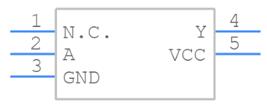
The following figure is SN74LVC1G17DCKR Pinout.
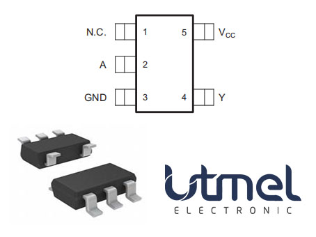
Pinout
| Pin Number | Pin Name | Description |
| 1 | NC | Not connected |
| 2 | A | Input |
| 3 | GND | Ground |
| 4 | Y | Output |
| 5 | VCC | Power terminal |
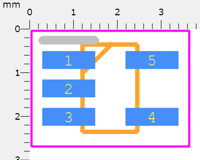
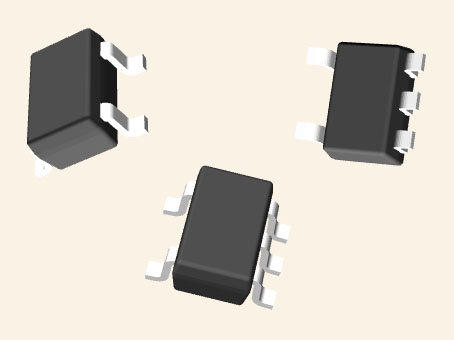
SN74LVC1G17DCKR CAD Model
SN74LVC1G17DCKR Features
• Available in Ultra Small 0.64-mm2
Package (DPW) With 0.5-mm Pitch
• Supports 5-V VCC Operation
• Inputs Accept Voltages to 5.5 V
• Max tpd of 4.6 ns at 3.3 V
• Low Power Consumption, 10-μA Max ICC
• ±24-mA Output Drive at 3.3 V
• Ioff Supports Live Insertion, Partial-Power-Down Mode, and Back-Drive Protection
• Latch-Up Performance Exceeds 100 mA Per JESD 78, Class II
• ESD Protection Exceeds JESD 22
– 2000-V Human-Body Model (A114-A)
– 200-V Machine Model (A115-A)
– 1000-V Charged-Device Model (C101)
Specifications
- TypeParameter
Parts with Similar Specs
SN74LVC1G17DCKR Functional Block Diagram
SN74LVC1G17DCKR Simplified Schematic
SN74LVC1G17DCKR Typical Application
This device features a balanced output drive and is based on CMOS technology.
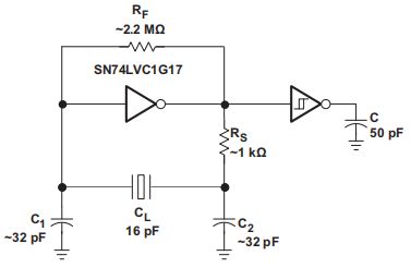
Typical Application
Bus congestion should be avoided at all costs because it can cause currents to exceed permissible limits. To avoid ringing, the high drive will cause quick edges into mild loads, hence routing and load circumstances should be considered.
SN74LVC1G17DCKR Layout
Inputs should never float when using multiple-bit logic devices. When just two inputs of a triple-input AND gate are used, or only three of the four buffer gates are used, many functions or parts of the functions of digital logic devices are unused. The undefined voltages at the outside connections result in undefined operating states, hence such input terminals should not be left disconnected. The rules that must be followed in all instances are listed below. To prevent floating, all unused inputs of digital logic devices must be connected to a high or low bias. The logic level that should be applied to any given unused input is determined by the device's function. They'll usually be connected to GND or Vcc, depending on which makes more sense or is more convenient.

Layout
SN74LVC1G17DCKR Alternatives
| Part Number | Description | Manufacturer |
| 74LVC1G17SE-7LOGIC | Buffer, LVC/LCX/Z Series, 1-Func, 1-Input, CMOS, PDSO5, SOT-353, 5 PIN | Diodes Incorporated |
| TC7SZ17FULOGIC | IC LVC/LCX/Z SERIES, 1-INPUT NON-INVERT GATE, PDSO5, 0.65 MM PITCH, PLASTIC, SSOP-5, Gate | Toshiba America Electronic Components |
| 74LVC1G17GWLOGIC | Buffer, CMOS, PDSO5 | Philips Semiconductors |
| SN74LVC1G17DCK3LOGIC | Single 1.65-V to 5.5-V buffer with Schmitt-Trigger inputs 5-SC70 -40 to 85 | Texas Instruments |
SN74LVC1G17DCKR Applications
• AV Receiver
• Audio Dock: Portable
• Blu-ray Player and Home Theater
• MP3 Player/Recorder
• Personal Digital Assistant (PDA)
• Power: Telecom/Server AC/DC Supply: Single Controller: Analog and Digital
• Solid State Drive (SSD): Client and Enterprise
• TV: LCD/Digital and High-Definition (HDTV)
• Tablet: Enterprise
• Video Analytics: Server
• Wireless Headset, Keyboard, and Mouse
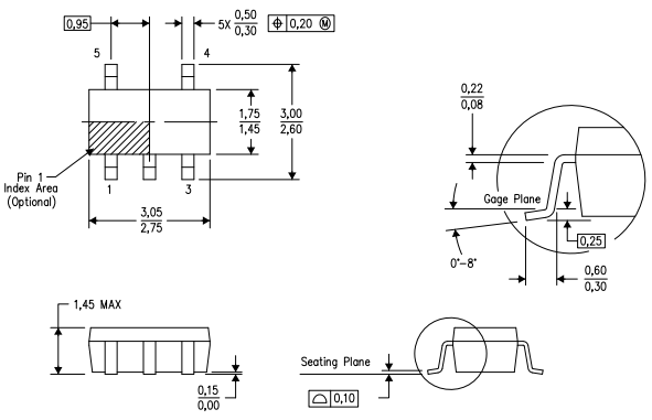
SN74LVC1G17DCKR Package
SN74LVC1G17DCKR Manufacturer
Texas Instruments Incorporated (TI) is a Texas-based technology company that designs and manufactures semiconductors and integrated circuits for electronic designers and manufacturers all over the world. Texas Instruments was founded in 1951 after a reorganization of Geophysical Service Incorporated, a firm founded in 1930 that developed seismic and defense electronics equipment.
Trend Analysis
What does the Schmitt trigger do?
Schmitt trigger devices are typically used in signal conditioning applications to remove noise from signals used in digital circuits, particularly mechanical contact bounce in switches.
What does the Schmitt-trigger buffer operate between?
1.65 and 5.5 V VCC.
What is the Boolean operation of the SN74LVC1G17DCKR?
Y = A.
What does the CMOS device have over a wide Vcc operating range?
High output drive.
What is the body size of the ultra-compact DPW packaging?
0.8 mm 0.8 mm.
Why does the SN74LVC1G17DCKR work as a standalone buffer?
Schmitt action.
What is the DPW package technology a significant advancement in?
IC packaging.
What is the compact size of the DPW package?
0.64 mm square footprint.
What type of applications is the SN74LVC1G17DCKR completely qualified for?
Partial-power-down.
What disables the outputs of the SN74LVC1G17DCKR?
The Ioff circuitry.
 PSoC™ Mixed Signal Array - CY8C22113 and CY8C22213 Microcontrollers: Technical Overview and Features
29 February 2024115
 LIS2DHTR Motion Sensor: 3-Axis, Application Hint, Datasheet PDF
23 February 20221343
 Achieving Studio-Grade Audio with the AD797: Ultralow Noise Op Amp Deep Dive
05 February 202653
![KSZ8721BL Transceiver RMII 48-LQFP [FAQ]: Pinout, Datasheet, and KS8721BL vs KSZ8721B vs KSZ8721BL](https://res.utmel.com/Images/Article/7da9d407-8d8a-4adb-ba6f-bc4159bfe56a.jpg) KSZ8721BL Transceiver RMII 48-LQFP [FAQ]: Pinout, Datasheet, and KS8721BL vs KSZ8721B vs KSZ8721BL
KSZ8721BL Transceiver RMII 48-LQFP [FAQ]: Pinout, Datasheet, and KS8721BL vs KSZ8721B vs KSZ8721BL08 March 2022976
 PN2222 Transistor: Pinout, Datasheet and Equivalent
20 July 202110400
 BC109 NPN Transistor: Pinout, Datasheet pdf and Equivalents
29 November 202114169
 A Comprehensive Guide to LTC699IS8#TRPBF - Simple Reset/Power-On Reset Supervisor
06 March 2024170
 LM4040 Bandgap Reference: Pinout, Equivalent and Datasheet
28 October 20212150
 13 Semiconductor Startups Poised for Success in 2024, According to Investors
11 December 20234310
 Transfer Learning Method for detailed defect classification in semiconductor manufacturing based on Convolution Neural Network
13 January 20231972
 Development Board History and Differences from Single Board Computers (SBCs)
16 May 20224092
 Optimizing Energy Exchange with Vehicle-to-Grid Technology
25 April 20232853
 What is Universal Serial Bus (USB)?
19 January 202610069
 Good news | Warm Congratulations to UTMEL Electronic for Obtaining the Letter of Authorization from XKB Connectivity
21 July 20252063
 Examining the performance of SiC inverter and DC-DC Converter Systems over Si
21 March 20233141
 The Impact of SMPS on LED Lighting and Diverse Industries
05 June 2025779
In Stock
United States
China
Canada
Japan
Russia
Germany
United Kingdom
Singapore
Italy
Hong Kong(China)
Taiwan(China)
France
Korea
Mexico
Netherlands
Malaysia
Austria
Spain
Switzerland
Poland
Thailand
Vietnam
India
United Arab Emirates
Afghanistan
Åland Islands
Albania
Algeria
American Samoa
Andorra
Angola
Anguilla
Antigua & Barbuda
Argentina
Armenia
Aruba
Australia
Azerbaijan
Bahamas
Bahrain
Bangladesh
Barbados
Belarus
Belgium
Belize
Benin
Bermuda
Bhutan
Bolivia
Bonaire, Sint Eustatius and Saba
Bosnia & Herzegovina
Botswana
Brazil
British Indian Ocean Territory
British Virgin Islands
Brunei
Bulgaria
Burkina Faso
Burundi
Cabo Verde
Cambodia
Cameroon
Cayman Islands
Central African Republic
Chad
Chile
Christmas Island
Cocos (Keeling) Islands
Colombia
Comoros
Congo
Congo (DRC)
Cook Islands
Costa Rica
Côte d’Ivoire
Croatia
Cuba
Curaçao
Cyprus
Czechia
Denmark
Djibouti
Dominica
Dominican Republic
Ecuador
Egypt
El Salvador
Equatorial Guinea
Eritrea
Estonia
Eswatini
Ethiopia
Falkland Islands
Faroe Islands
Fiji
Finland
French Guiana
French Polynesia
Gabon
Gambia
Georgia
Ghana
Gibraltar
Greece
Greenland
Grenada
Guadeloupe
Guam
Guatemala
Guernsey
Guinea
Guinea-Bissau
Guyana
Haiti
Honduras
Hungary
Iceland
Indonesia
Iran
Iraq
Ireland
Isle of Man
Israel
Jamaica
Jersey
Jordan
Kazakhstan
Kenya
Kiribati
Kosovo
Kuwait
Kyrgyzstan
Laos
Latvia
Lebanon
Lesotho
Liberia
Libya
Liechtenstein
Lithuania
Luxembourg
Macao(China)
Madagascar
Malawi
Maldives
Mali
Malta
Marshall Islands
Martinique
Mauritania
Mauritius
Mayotte
Micronesia
Moldova
Monaco
Mongolia
Montenegro
Montserrat
Morocco
Mozambique
Myanmar
Namibia
Nauru
Nepal
New Caledonia
New Zealand
Nicaragua
Niger
Nigeria
Niue
Norfolk Island
North Korea
North Macedonia
Northern Mariana Islands
Norway
Oman
Pakistan
Palau
Palestinian Authority
Panama
Papua New Guinea
Paraguay
Peru
Philippines
Pitcairn Islands
Portugal
Puerto Rico
Qatar
Réunion
Romania
Rwanda
Samoa
San Marino
São Tomé & Príncipe
Saudi Arabia
Senegal
Serbia
Seychelles
Sierra Leone
Sint Maarten
Slovakia
Slovenia
Solomon Islands
Somalia
South Africa
South Sudan
Sri Lanka
St Helena, Ascension, Tristan da Cunha
St. Barthélemy
St. Kitts & Nevis
St. Lucia
St. Martin
St. Pierre & Miquelon
St. Vincent & Grenadines
Sudan
Suriname
Svalbard & Jan Mayen
Sweden
Syria
Tajikistan
Tanzania
Timor-Leste
Togo
Tokelau
Tonga
Trinidad & Tobago
Tunisia
Turkey
Turkmenistan
Turks & Caicos Islands
Tuvalu
U.S. Outlying Islands
U.S. Virgin Islands
Uganda
Ukraine
Uruguay
Uzbekistan
Vanuatu
Vatican City
Venezuela
Wallis & Futuna
Yemen
Zambia
Zimbabwe


