
 Product
 Brand
Brand Articles
 Tools
Tools
TDA2822M Low-Voltage Power Amplifier: Datasheet, Pinout and Circuit

1A mA 2W W Audio Amplifiers 3.32mm mm 6.6mm mm 1.4W W 15V V 8 pins 8-DIP (0.300, 7.62mm)


1A mA 2W W Audio Amplifiers 3.32mm mm 6.6mm mm 1.4W W 15V V 8 pins 8-DIP (0.300, 7.62mm)
TDA2822M is a Dual low-voltage power amplifier. This post mainly covers the datasheet, power, circuit, pinout, replacement, and more details about the TDA2822M voltage amplifier. Furthermore, there is a huge range of semiconductors, capacitors, resistors, and ICs in stock. Welcome your RFQ!

Stereo Audio amplifier Using Tda2822
TDA2822M Description
The TDA2822M is a Dual low-voltage power amplifier in an 8-Dip Minidip monolithic integrated circuit. It's designed to be used in portable tape players and radios as a dual audio power amplifier.
TDA2822M Pinout

TDA2822M Pinout
| Pin# | Pin Name | Pin Description |
| 1 | Output 1 | Output 1 of the IC to drive a speaker |
| 2 | Vcc | Positive Supply Connection of the IC |
| 3 | Output 2 | Output 2 of the IC to drive a speaker |
| 4 | Ground (GND) | Ground / Negative For Both Amplifiers |
| 5 | Input 2 (+) | Inverting Input 2 of the IC |
| 6 | Input 2 (-) | Non-Inverting 2 Input of IC |
| 7 | Input 1 (+) | Non-Inverting Input 1 of IC |
| 8 | Input 2 (-) | Inverting Input 1 of the IC |
TDA2822M CAD Model
Symbol

TDA2822M Symbol
Footprint

TDA2822M Footprint
3D Model

TDA2822M 3D Model
TDA2822M Schematics Diagram

TDA2822M Schematics Diagram
Specifications
- TypeParameter
- Mount
In electronic components, the term "Mount" typically refers to the method or process of physically attaching or fixing a component onto a circuit board or other electronic device. This can involve soldering, adhesive bonding, or other techniques to secure the component in place. The mounting process is crucial for ensuring proper electrical connections and mechanical stability within the electronic system. Different components may have specific mounting requirements based on their size, shape, and function, and manufacturers provide guidelines for proper mounting procedures to ensure optimal performance and reliability of the electronic device.
Through Hole - Mounting Type
The "Mounting Type" in electronic components refers to the method used to attach or connect a component to a circuit board or other substrate, such as through-hole, surface-mount, or panel mount.
Through Hole - Package / Case
refers to the protective housing that encases an electronic component, providing mechanical support, electrical connections, and thermal management.
8-DIP (0.300, 7.62mm) - Number of Pins8
- Manufacturer Package Identifier
The Manufacturer Package Identifier is a unique code or label assigned by the manufacturer to identify a specific package or housing style of an electronic component. This identifier helps in distinguishing between different package types of the same component, such as integrated circuits, transistors, or diodes. It typically includes information about the package dimensions, lead configuration, and other physical characteristics of the component. The Manufacturer Package Identifier is crucial for ensuring compatibility and proper assembly of electronic components in various devices and circuits.
8-Mini DIP - Operating Temperature
The operating temperature is the range of ambient temperature within which a power supply, or any other electrical equipment, operate in. This ranges from a minimum operating temperature, to a peak or maximum operating temperature, outside which, the power supply may fail.
-40°C~150°C TJ - Packaging
Semiconductor package is a carrier / shell used to contain and cover one or more semiconductor components or integrated circuits. The material of the shell can be metal, plastic, glass or ceramic.
Tube - JESD-609 Code
The "JESD-609 Code" in electronic components refers to a standardized marking code that indicates the lead-free solder composition and finish of electronic components for compliance with environmental regulations.
e3 - Pbfree Code
The "Pbfree Code" parameter in electronic components refers to the code or marking used to indicate that the component is lead-free. Lead (Pb) is a toxic substance that has been widely used in electronic components for many years, but due to environmental concerns, there has been a shift towards lead-free alternatives. The Pbfree Code helps manufacturers and users easily identify components that do not contain lead, ensuring compliance with regulations and promoting environmentally friendly practices. It is important to pay attention to the Pbfree Code when selecting electronic components to ensure they meet the necessary requirements for lead-free applications.
yes - Part Status
Parts can have many statuses as they progress through the configuration, analysis, review, and approval stages.
Obsolete - Moisture Sensitivity Level (MSL)
Moisture Sensitivity Level (MSL) is a standardized rating that indicates the susceptibility of electronic components, particularly semiconductors, to moisture-induced damage during storage and the soldering process, defining the allowable exposure time to ambient conditions before they require special handling or baking to prevent failures
1 (Unlimited) - Number of Terminations8
- ECCN Code
An ECCN (Export Control Classification Number) is an alphanumeric code used by the U.S. Bureau of Industry and Security to identify and categorize electronic components and other dual-use items that may require an export license based on their technical characteristics and potential for military use.
EAR99 - TypeClass AB
- Terminal Finish
Terminal Finish refers to the surface treatment applied to the terminals or leads of electronic components to enhance their performance and longevity. It can improve solderability, corrosion resistance, and overall reliability of the connection in electronic assemblies. Common finishes include nickel, gold, and tin, each possessing distinct properties suitable for various applications. The choice of terminal finish can significantly impact the durability and effectiveness of electronic devices.
Matte Tin (Sn) - annealed - Max Power Dissipation
The maximum power that the MOSFET can dissipate continuously under the specified thermal conditions.
1.4W - Voltage - Supply
Voltage - Supply refers to the range of voltage levels that an electronic component or circuit is designed to operate with. It indicates the minimum and maximum supply voltage that can be applied for the device to function properly. Providing supply voltages outside this range can lead to malfunction, damage, or reduced performance. This parameter is critical for ensuring compatibility between different components in a circuit.
1.8V~15V - Terminal Position
In electronic components, the term "Terminal Position" refers to the physical location of the connection points on the component where external electrical connections can be made. These connection points, known as terminals, are typically used to attach wires, leads, or other components to the main body of the electronic component. The terminal position is important for ensuring proper connectivity and functionality of the component within a circuit. It is often specified in technical datasheets or component specifications to help designers and engineers understand how to properly integrate the component into their circuit designs.
DUAL - Number of Functions2
- Base Part Number
The "Base Part Number" (BPN) in electronic components serves a similar purpose to the "Base Product Number." It refers to the primary identifier for a component that captures the essential characteristics shared by a group of similar components. The BPN provides a fundamental way to reference a family or series of components without specifying all the variations and specific details.
TDA2822 - Pin Count
a count of all of the component leads (or pins)
8 - Output Type
The "Output Type" parameter in electronic components refers to the type of signal or data that is produced by the component as an output. This parameter specifies the nature of the output signal, such as analog or digital, and can also include details about the voltage levels, current levels, frequency, and other characteristics of the output signal. Understanding the output type of a component is crucial for ensuring compatibility with other components in a circuit or system, as well as for determining how the output signal can be utilized or processed further. In summary, the output type parameter provides essential information about the nature of the signal that is generated by the electronic component as its output.
1-Channel (Mono) or 2-Channel (Stereo) - Operating Supply Voltage
The voltage level by which an electrical system is designated and to which certain operating characteristics of the system are related.
12V - Supply Voltage-Max (Vsup)
The parameter "Supply Voltage-Max (Vsup)" in electronic components refers to the maximum voltage that can be safely applied to the component without causing damage. It is an important specification to consider when designing or using electronic circuits to ensure the component operates within its safe operating limits. Exceeding the maximum supply voltage can lead to overheating, component failure, or even permanent damage. It is crucial to adhere to the specified maximum supply voltage to ensure the reliable and safe operation of the electronic component.
15V - Number of Channels2
- Nominal Supply Current
Nominal current is the same as the rated current. It is the current drawn by the motor while delivering rated mechanical output at its shaft.
1A - Power Dissipation
the process by which an electronic or electrical device produces heat (energy loss or waste) as an undesirable derivative of its primary action.
1.4W - Output Current
The rated output current is the maximum load current that a power supply can provide at a specified ambient temperature. A power supply can never provide more current that it's rated output current unless there is a fault, such as short circuit at the load.
1A - Output Power
That power available at a specified output of a device under specified conditions of operation.
650mW - Supply Type
Supply Type in electronic components refers to the classification of power sources used to operate the component. It indicates whether the component requires DC or AC power, and if DC, specifies the voltage levels such as low, medium, or high. Different supply types can affect the performance, compatibility, and application of the component in electronic circuits. Understanding the supply type is crucial for proper component selection and integration into electronic designs.
Single - Voltage Gain
Voltage gain is a measure of how much an electronic component or circuit amplifies an input voltage signal to produce an output voltage signal. It is typically expressed as a ratio or in decibels (dB). A higher voltage gain indicates a greater amplification of the input signal. Voltage gain is an important parameter in amplifiers, where it determines the level of amplification provided by the circuit. It is calculated by dividing the output voltage by the input voltage and is a key factor in determining the overall performance and functionality of electronic devices.
39dB - Power Supply Rejection Ratio (PSRR)
Power Supply Rejection Ratio (PSRR) is a measure of how well an electronic component, such as an operational amplifier or voltage regulator, can reject changes in its supply voltage. It indicates the ability of the component to maintain a stable output voltage despite fluctuations in the input supply voltage. A higher PSRR value signifies better performance in rejecting noise and variations from the power supply, leading to improved signal integrity and more reliable operation in electronic circuits. PSRR is typically expressed in decibels (dB).
40dB - Gain
In electronic components, "Gain" refers to the ratio of the output signal amplitude to the input signal amplitude. It is a measure of the amplification provided by the component, such as a transistor or operational amplifier. Gain is typically expressed in decibels (dB) or as a numerical value, indicating how much the signal is amplified by the component.A higher gain value indicates a greater amplification of the input signal, while a lower gain value indicates less amplification. Gain is an important parameter in designing and analyzing electronic circuits, as it determines the overall performance and functionality of the system. Different components have different gain characteristics, and understanding the gain of a component is crucial for achieving the desired signal processing or amplification in electronic systems.
39 dB - Max Output Power
The maximum output power = the maximum output current × the rated output voltage
2W - Input Bias Current
Input Bias Current refers to the small amount of current that flows into the input terminals of an electronic component, such as an operational amplifier. It is primarily caused by the input impedance of the device and the characteristics of the transistors within it. This current is crucial in determining the accuracy of the analog signal processing, as it can affect the level of voltage offset and signal integrity in the application. In many precise applications, minimizing input bias current is essential to achieve optimal performance.
100nA - Max Output Power x Channels @ Load
Max Output Power x Channels @ Load is a specification that describes the maximum power output that an electronic component, such as an amplifier or audio device, can deliver across a certain number of channels at a specific load impedance. This parameter is important for understanding the capability of the component to drive speakers or other devices effectively. The value is typically expressed in watts and can vary depending on the number of channels being used and the impedance of the load. It helps users determine the compatibility of the component with their audio setup and ensures that the component can provide sufficient power for optimal performance.
2W x 1 @ 16 Ω; 1W x 2 @ 8 Ω - Harmonic Distortion
Harmonic distortion is a common parameter used to describe the quality of audio or electronic signals. It refers to the presence of unwanted harmonics or additional frequencies in the output signal that were not present in the input signal. These harmonics are typically multiples of the original signal frequency and can distort the waveform, affecting the overall sound quality or performance of the electronic component. Lower harmonic distortion values indicate a cleaner and more accurate output signal, while higher distortion levels can result in a more distorted or altered sound. Manufacturers often specify harmonic distortion levels in percentage or decibels to help users understand the quality of the component's output.
10% - Load Impedance
Load impedance is a crucial parameter in electronic components that refers to the impedance presented by the load to the output of a circuit or device. It is a measure of how much the load resists the flow of current from the source. Load impedance is typically expressed in ohms and can greatly affect the performance and efficiency of a circuit. Matching the load impedance to the source impedance is important for maximum power transfer and signal integrity in electronic systems. Failure to properly match load impedance can result in signal distortion, power loss, and reduced overall performance of the circuit.
4Ohm - Height3.32mm
- Length10.92mm
- Width6.6mm
- REACH SVHC
The parameter "REACH SVHC" in electronic components refers to the compliance with the Registration, Evaluation, Authorization, and Restriction of Chemicals (REACH) regulation regarding Substances of Very High Concern (SVHC). SVHCs are substances that may have serious effects on human health or the environment, and their use is regulated under REACH to ensure their safe handling and minimize their impact.Manufacturers of electronic components need to declare if their products contain any SVHCs above a certain threshold concentration and provide information on the safe use of these substances. This information allows customers to make informed decisions about the potential risks associated with using the components and take appropriate measures to mitigate any hazards.Ensuring compliance with REACH SVHC requirements is essential for electronics manufacturers to meet regulatory standards, protect human health and the environment, and maintain transparency in their supply chain. It also demonstrates a commitment to sustainability and responsible manufacturing practices in the electronics industry.
No SVHC - Radiation Hardening
Radiation hardening is the process of making electronic components and circuits resistant to damage or malfunction caused by high levels of ionizing radiation, especially for environments in outer space (especially beyond the low Earth orbit), around nuclear reactors and particle accelerators, or during nuclear accidents or nuclear warfare.
No - RoHS Status
RoHS means “Restriction of Certain Hazardous Substances” in the “Hazardous Substances Directive” in electrical and electronic equipment.
ROHS3 Compliant - Lead Free
Lead Free is a term used to describe electronic components that do not contain lead as part of their composition. Lead is a toxic material that can have harmful effects on human health and the environment, so the electronics industry has been moving towards lead-free components to reduce these risks. Lead-free components are typically made using alternative materials such as silver, copper, and tin. Manufacturers must comply with regulations such as the Restriction of Hazardous Substances (RoHS) directive to ensure that their products are lead-free and environmentally friendly.
Lead Free
TDA2822M Features
Supply Voltage: 3-15V.
Output Power: 3.2 W.
Audio - Load Impedance: 8 Ohms.
Gain: 39 dB.
Operating Supply Current: 12 mA
Ib - Input Bias Current: 0.1 uA.
PSRR - Power Supply Rejection Ratio: 40 dB.
Available in 8-Pin DIP package
TDA2822M Circuit
TDA2822M Amplifier Test Circuit in Stereo Mode

Test Circuit in Stereo Mode
The left channel input is connected to the first built-in amplifier's non-inverting input (pin 1), while the right channel is connected to the second built-in amplifier's non-inverting input (pin 16). Separate 1000uF capacitors are used to link the inverting input of these built-in amplifiers to the ground (C5 and C6). Pins 6 and 11 of the IC control the amplified outputs (left and right). Capacitors C1 and C2 are used to connect the outputs to the matching speakers. The resistor-capacitor branch connected between speakers (0.1uF and 4.7 ohm) is intended to improve high-frequency stability and prevent oscillations. C7 is the power supply filter capacitor.
TDA2822M Amplifier Test Circuit in Bridge Mode

Test Circuit in Bridge Mode
The output power of the TDA2822M amplifier can be boosted by employing the bridge configuration in mono mode, as shown in Figure 2. The audio signal is fed into the first built-in amplifier's non-inverting input. The second built-in amplifier's non-inverting input is grounded. The C9, C11 capacitor branch grounds the inverting input of these amplifiers. The R5, C8, and R6, C10 branches are intended to improve high-frequency stability and reduce oscillations. C12 is a capacitor that filters the power source.
TDA2822M Applications
Audio amplifiers for radios
Computer Audio Amplifiers
Toys Audio Amplifiers
Battery Operated Music Players
Any Type of Low Power Audio Amplifier
TDA2822M Typical Application
How to Use TDA2822M

TDA2822M Circuit Diagram
The TDA2822M IC is used in the audio amplifier shown above. This is a mono audio amplifier circuit, but as previously stated, this IC can also be used to make a stereo amplifier circuit. With the IC, this circuit uses a few passive components. The operational voltage ranges between 3 and 15 volts DC. The 10K variable resistor will be connected to the audio input points specified in the design, which will be connected to the audio you want to amplify. A speaker with an impedance of 8 Ohms is connected between pins 1 and 3 of the IC.
For long-life performance, do not operate the IC at higher voltages than 15V, always protect the IC from short circuits, double-check the connection before applying power to the IC, do not apply more heat than the IC can handle while soldering, and make sure the IC is powered in the correct polarity or use a diode between the IC and the power supply. Always store and operate the IC at temperatures between -40 and +150 degrees Celsius.
TDA2822M Replacements
KA2209, KA2209B, S1A2209A01-D0B0, TDA2822M, LM380, NJM2073
TDA2822M Outline Dimensions

TDA2822M Outline Dimensions
TDA2822M Manufacturer
STMicroelectronics is a global independent semiconductor company and a leader in developing and delivering semiconductor solutions across the spectrum of microelectronics applications. An unrivaled combination of silicon and system expertise, manufacturing strength, Intellectual Property (IP) portfolio, and strategic partners’ positions, STMicroelectronics is at the forefront of System-on-Chip (SoC) technology and its products play a key role in enabling today's convergence trends.
Trend Analysis
Datasheet PDF
- Datasheets :
TDA2822M-STMicroelectronics-datasheet-10838733.pdf
TDA2822M-STMicroelectronics-datasheet-6396597.pdf
TDA2822M-STMicroelectronics-datasheet-72878.pdf
TDA2822M-STMicroelectronics-datasheet-104809.pdf
TDA2822M-STMicroelectronics-datasheet-14136903.pdf
pid_4771162_tda2822m-stmicroelectronics-datasheet-10838733.pdf
What is the use of TDA2822M?
The TDA2822M is a monolithic integrated circuit in 8 lead Mini dip package. It is intended for use as a dual audio power amplifier in portable cassette players and radios.
What is the difference between TDA2822 and TDA2822M?
The package of TDA2822 is the same as TDA2822M. The difference is that: TDA2822M can work from 3V to 15V, while the highest working voltage of TDA2822 is only 8V. The higher the voltage, the higher the output power, so the output power of TDA2822M can be higher (dual-channel).
What is the working voltage of TDA2822M?
Power Supply Voltage Max: 15V
Power Supply Voltage Min: 1.8V
Can the integrated circuits TDA2822L and TDA2822M be directly replaced?
The working voltage of TDA2822L is 1.8-12V, and the working voltage of TDA2822M is 1.8-15V. The others are the same. They can be used interchangeably within the working voltage range. Your radio should be powered under 9V. It should be directly replaceable. Just look at the power supply voltage before changing.
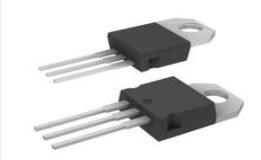 What is the difference between IRF640 and IRF740: IRF640 vs. IRF740
08 December 20217002
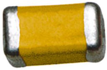 TDK C3216X5R1E476M160AC: 47µF MLCC Capacitor Review & Comparison
27 August 20252720
 A Comprehensive Guide to LTC7880IUKG#TRPBF DC/DC Switching Controller
06 March 2024329
 Microchip PIC18F26J50ISP Microcontroller Datasheet Overview
28 February 2024227
 STM32F030C8T6: Overview, Features and Datasheet
16 October 20236172
 BF494 Transistor: Circuits, Pinout, and Datasheet
30 December 202112170
 AD5700 HART Modem: Pinout, Features and Datasheet
18 January 20222842
 Vicor Corporation PI3740-00-LGIZ Purchase Checklist
16 August 2025280
 What are Graphene Transistors?
21 October 202510014
 Utmel, China's Leading Overseas Component Distributor, at PCIM Europe 2023
10 November 20237669
 Selection and Optimization of Peripheral Components for DC-DC Boost Regulator
15 April 20222274
 Chip Filters, Piezoelectric Materials and the Piezoelectric Effect
27 September 20226994
 What is ToF Technology?
22 January 20213532
 What is Low Pass Filter
18 November 20217326
 A brief Analysis of the 555 Timer Circuit and its Project Applications
15 March 20243322
 Vision Capabilities Are at the Heart of AI's Evolutionary Possession of Intelligence
06 July 20222296
STMicroelectronics
In Stock: 6470
United States
China
Canada
Japan
Russia
Germany
United Kingdom
Singapore
Italy
Hong Kong(China)
Taiwan(China)
France
Korea
Mexico
Netherlands
Malaysia
Austria
Spain
Switzerland
Poland
Thailand
Vietnam
India
United Arab Emirates
Afghanistan
Åland Islands
Albania
Algeria
American Samoa
Andorra
Angola
Anguilla
Antigua & Barbuda
Argentina
Armenia
Aruba
Australia
Azerbaijan
Bahamas
Bahrain
Bangladesh
Barbados
Belarus
Belgium
Belize
Benin
Bermuda
Bhutan
Bolivia
Bonaire, Sint Eustatius and Saba
Bosnia & Herzegovina
Botswana
Brazil
British Indian Ocean Territory
British Virgin Islands
Brunei
Bulgaria
Burkina Faso
Burundi
Cabo Verde
Cambodia
Cameroon
Cayman Islands
Central African Republic
Chad
Chile
Christmas Island
Cocos (Keeling) Islands
Colombia
Comoros
Congo
Congo (DRC)
Cook Islands
Costa Rica
Côte d’Ivoire
Croatia
Cuba
Curaçao
Cyprus
Czechia
Denmark
Djibouti
Dominica
Dominican Republic
Ecuador
Egypt
El Salvador
Equatorial Guinea
Eritrea
Estonia
Eswatini
Ethiopia
Falkland Islands
Faroe Islands
Fiji
Finland
French Guiana
French Polynesia
Gabon
Gambia
Georgia
Ghana
Gibraltar
Greece
Greenland
Grenada
Guadeloupe
Guam
Guatemala
Guernsey
Guinea
Guinea-Bissau
Guyana
Haiti
Honduras
Hungary
Iceland
Indonesia
Iran
Iraq
Ireland
Isle of Man
Israel
Jamaica
Jersey
Jordan
Kazakhstan
Kenya
Kiribati
Kosovo
Kuwait
Kyrgyzstan
Laos
Latvia
Lebanon
Lesotho
Liberia
Libya
Liechtenstein
Lithuania
Luxembourg
Macao(China)
Madagascar
Malawi
Maldives
Mali
Malta
Marshall Islands
Martinique
Mauritania
Mauritius
Mayotte
Micronesia
Moldova
Monaco
Mongolia
Montenegro
Montserrat
Morocco
Mozambique
Myanmar
Namibia
Nauru
Nepal
New Caledonia
New Zealand
Nicaragua
Niger
Nigeria
Niue
Norfolk Island
North Korea
North Macedonia
Northern Mariana Islands
Norway
Oman
Pakistan
Palau
Palestinian Authority
Panama
Papua New Guinea
Paraguay
Peru
Philippines
Pitcairn Islands
Portugal
Puerto Rico
Qatar
Réunion
Romania
Rwanda
Samoa
San Marino
São Tomé & Príncipe
Saudi Arabia
Senegal
Serbia
Seychelles
Sierra Leone
Sint Maarten
Slovakia
Slovenia
Solomon Islands
Somalia
South Africa
South Sudan
Sri Lanka
St Helena, Ascension, Tristan da Cunha
St. Barthélemy
St. Kitts & Nevis
St. Lucia
St. Martin
St. Pierre & Miquelon
St. Vincent & Grenadines
Sudan
Suriname
Svalbard & Jan Mayen
Sweden
Syria
Tajikistan
Tanzania
Timor-Leste
Togo
Tokelau
Tonga
Trinidad & Tobago
Tunisia
Turkey
Turkmenistan
Turks & Caicos Islands
Tuvalu
U.S. Outlying Islands
U.S. Virgin Islands
Uganda
Ukraine
Uruguay
Uzbekistan
Vanuatu
Vatican City
Venezuela
Wallis & Futuna
Yemen
Zambia
Zimbabwe


