
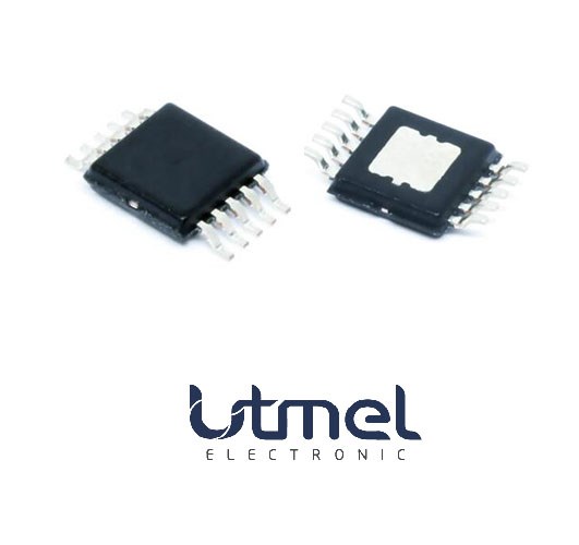
 Product
 Brand
Brand Articles
 Tools
Tools
74HCT04 Hex inverter IC: Where & How to use 74HCT04


Gates & Inverters 4mA mA 4.5V~5.5V V
The 74HCT04 is a hex inverter, high-speed CMOS device, low-power Schottky TTL circuit. Furthermore, Huge range of Semiconductors, Capacitors, Resistors and IcS in stock. Welcome RFQ.
- 74HCT04 Pinout
- 74HCT04 CAD Model
- 74HCT04 Overview
- 74HCT04 Features
- Specifications
- 74HCT04 Functional Block Diagram
- 74HCT04 Equivalent
- 74HCT04 Alternatives Logic Gate IC
- Where to use 74HCT04 Hex Inverter
- How to Use 74HCT04 IC
- 74HCT04 Propagation Delay
- 74HCT04 Application
- 74HCT04 Package
- 74HCT04 Manufacturer
- Datasheet PDF
- Trend Analysis
74HCT04 Pinout

Pinout
| Symbol | Pin | Description |
| 1A, 2A, 3A, 4A, 5A, 6A | 1, 3, 5, 9, 11, 13 | data input |
| 1Y, 2Y, 3Y, 4Y, 5Y, 6Y | 2, 4, 6, 8, 10, 12 | data output |
| GND | 7 | ground (0 V) |
| VCC | 14 | supply voltage |
Pin description
74HCT04 CAD Model

Symbol

Footprint

3D Model
74HCT04 Overview
The 74HCT04 IC is a hex inverter IC which is composed of six independent inverters with standard push-pull outputs. It is a high-speed inverter whose pins are low power Schottky (LSTTL) compatible. All the inputs are protected from electric discharges through the diodes protection network which provides protection from input voltages in excess of Vcc by enabling the use of current limiting resistors. It can operate within a range of -40°C to +125°C.
The 74HCT04 is a high-speed CMOS hex inverter, HCT means high-speed CMOS architecture TTL level. The level of the chip adopts TTL level. If the speed requirement is not high, 74LS04 can be used instead. The inputs include clamp diodes that enable the use of current limiting resistors to interface inputs to voltages in excess of VCC.
This article provides you with a basic overview of the 74HCT04, including its pin descriptions, features and specifications, etc., to help you quickly understand what 74HCT04 is.
74HCT04 Features
● Hex Inverter IC with a voltage range of 4.5V to 5.5V
● Schmitt triggered inputs and is compatible with the TTL voltage level which allows unlimited rise and fall times.
● Sinks or Sources 4mA at Vcc= 4.5V
● CMOS logic-based with a feature of low power consumption
● Continuous Output Current: ±25mA
● Maximum Propagation Delay is 29 ns
● Min HIGH-level input voltage is 2V
● Max LOW-level input voltage is 0.8V
● Available in SO-14 and TSSOP-14 packages
● Totally Lead-Free & Fully RoHS Compliant
Specifications
- TypeParameter
- Factory Lead Time4 Weeks
- Mounting Type
The "Mounting Type" in electronic components refers to the method used to attach or connect a component to a circuit board or other substrate, such as through-hole, surface-mount, or panel mount.
Surface Mount - Package / Case
refers to the protective housing that encases an electronic component, providing mechanical support, electrical connections, and thermal management.
14-SOIC (0.154, 3.90mm Width) - Surface Mount
having leads that are designed to be soldered on the side of a circuit board that the body of the component is mounted on.
YES - Number of Pins14
- Logic Level-High2V
- Logic Level-Low0.8V
- Operating Temperature
The operating temperature is the range of ambient temperature within which a power supply, or any other electrical equipment, operate in. This ranges from a minimum operating temperature, to a peak or maximum operating temperature, outside which, the power supply may fail.
-40°C~125°C - Packaging
Semiconductor package is a carrier / shell used to contain and cover one or more semiconductor components or integrated circuits. The material of the shell can be metal, plastic, glass or ceramic.
Tube - Series
In electronic components, the "Series" refers to a group of products that share similar characteristics, designs, or functionalities, often produced by the same manufacturer. These components within a series typically have common specifications but may vary in terms of voltage, power, or packaging to meet different application needs. The series name helps identify and differentiate between various product lines within a manufacturer's catalog.
74HCT - JESD-609 Code
The "JESD-609 Code" in electronic components refers to a standardized marking code that indicates the lead-free solder composition and finish of electronic components for compliance with environmental regulations.
e4 - Part Status
Parts can have many statuses as they progress through the configuration, analysis, review, and approval stages.
Active - Moisture Sensitivity Level (MSL)
Moisture Sensitivity Level (MSL) is a standardized rating that indicates the susceptibility of electronic components, particularly semiconductors, to moisture-induced damage during storage and the soldering process, defining the allowable exposure time to ambient conditions before they require special handling or baking to prevent failures
1 (Unlimited) - Number of Terminations14
- ECCN Code
An ECCN (Export Control Classification Number) is an alphanumeric code used by the U.S. Bureau of Industry and Security to identify and categorize electronic components and other dual-use items that may require an export license based on their technical characteristics and potential for military use.
EAR99 - Terminal Finish
Terminal Finish refers to the surface treatment applied to the terminals or leads of electronic components to enhance their performance and longevity. It can improve solderability, corrosion resistance, and overall reliability of the connection in electronic assemblies. Common finishes include nickel, gold, and tin, each possessing distinct properties suitable for various applications. The choice of terminal finish can significantly impact the durability and effectiveness of electronic devices.
Nickel/Palladium/Gold (Ni/Pd/Au) - HTS Code
HTS (Harmonized Tariff Schedule) codes are product classification codes between 8-1 digits. The first six digits are an HS code, and the countries of import assign the subsequent digits to provide additional classification. U.S. HTS codes are 1 digits and are administered by the U.S. International Trade Commission.
8542.39.00.01 - Voltage - Supply
Voltage - Supply refers to the range of voltage levels that an electronic component or circuit is designed to operate with. It indicates the minimum and maximum supply voltage that can be applied for the device to function properly. Providing supply voltages outside this range can lead to malfunction, damage, or reduced performance. This parameter is critical for ensuring compatibility between different components in a circuit.
4.5V~5.5V - Terminal Position
In electronic components, the term "Terminal Position" refers to the physical location of the connection points on the component where external electrical connections can be made. These connection points, known as terminals, are typically used to attach wires, leads, or other components to the main body of the electronic component. The terminal position is important for ensuring proper connectivity and functionality of the component within a circuit. It is often specified in technical datasheets or component specifications to help designers and engineers understand how to properly integrate the component into their circuit designs.
DUAL - Terminal Form
Occurring at or forming the end of a series, succession, or the like; closing; concluding.
GULL WING - Peak Reflow Temperature (Cel)
Peak Reflow Temperature (Cel) is a parameter that specifies the maximum temperature at which an electronic component can be exposed during the reflow soldering process. Reflow soldering is a common method used to attach electronic components to a circuit board. The Peak Reflow Temperature is crucial because it ensures that the component is not damaged or degraded during the soldering process. Exceeding the specified Peak Reflow Temperature can lead to issues such as component failure, reduced performance, or even permanent damage to the component. It is important for manufacturers and assemblers to adhere to the recommended Peak Reflow Temperature to ensure the reliability and functionality of the electronic components.
NOT SPECIFIED - Number of Functions6
- Supply Voltage
Supply voltage refers to the electrical potential difference provided to an electronic component or circuit. It is crucial for the proper operation of devices, as it powers their functions and determines performance characteristics. The supply voltage must be within specified limits to ensure reliability and prevent damage to components. Different electronic devices have specific supply voltage requirements, which can vary widely depending on their design and intended application.
5V - Terminal Pitch
The center distance from one pole to the next.
1.27mm - Time@Peak Reflow Temperature-Max (s)
Time@Peak Reflow Temperature-Max (s) refers to the maximum duration that an electronic component can be exposed to the peak reflow temperature during the soldering process, which is crucial for ensuring reliable solder joint formation without damaging the component.
NOT SPECIFIED - Base Part Number
The "Base Part Number" (BPN) in electronic components serves a similar purpose to the "Base Product Number." It refers to the primary identifier for a component that captures the essential characteristics shared by a group of similar components. The BPN provides a fundamental way to reference a family or series of components without specifying all the variations and specific details.
74HCT04 - Pin Count
a count of all of the component leads (or pins)
14 - Supply Voltage-Max (Vsup)
The parameter "Supply Voltage-Max (Vsup)" in electronic components refers to the maximum voltage that can be safely applied to the component without causing damage. It is an important specification to consider when designing or using electronic circuits to ensure the component operates within its safe operating limits. Exceeding the maximum supply voltage can lead to overheating, component failure, or even permanent damage. It is crucial to adhere to the specified maximum supply voltage to ensure the reliable and safe operation of the electronic component.
5.5V - Supply Voltage-Min (Vsup)
The parameter "Supply Voltage-Min (Vsup)" in electronic components refers to the minimum voltage level required for the component to operate within its specified performance range. This parameter indicates the lowest voltage that can be safely applied to the component without risking damage or malfunction. It is crucial to ensure that the supply voltage provided to the component meets or exceeds this minimum value to ensure proper functionality and reliability. Failure to adhere to the specified minimum supply voltage may result in erratic behavior, reduced performance, or even permanent damage to the component.
4.5V - Number of Circuits6
- Output Current
The rated output current is the maximum load current that a power supply can provide at a specified ambient temperature. A power supply can never provide more current that it's rated output current unless there is a fault, such as short circuit at the load.
4mA - Family
In electronic components, the parameter "Family" typically refers to a categorization or classification system used to group similar components together based on their characteristics, functions, or applications. This classification helps users easily identify and select components that meet their specific requirements. The "Family" parameter can include various subcategories such as resistors, capacitors, diodes, transistors, integrated circuits, and more. Understanding the "Family" of an electronic component can provide valuable information about its compatibility, performance specifications, and potential uses within a circuit or system. It is important to consider the "Family" parameter when designing or troubleshooting electronic circuits to ensure proper functionality and compatibility with other components.
HCT - Logic Type
Logic Type in electronic components refers to the classification of circuits based on the logical operations they perform. It includes types such as AND, OR, NOT, NAND, NOR, XOR, and XNOR, each defining the relationship between binary inputs and outputs. The logic type determines how the inputs affect the output state based on specific rules of Boolean algebra. This classification is crucial for designing digital circuits and systems, enabling engineers to select appropriate components for desired functionalities.
Inverter - Max Propagation Delay @ V, Max CL
The parameter "Max Propagation Delay @ V, Max CL" in electronic components refers to the maximum amount of time it takes for a signal to propagate through the component from input to output when operating at a specific voltage (V) and driving a maximum specified load capacitance (CL). This parameter is crucial in determining the speed and performance of the component in a circuit. A shorter propagation delay indicates faster signal processing and better overall performance. Designers use this parameter to ensure that signals can be transmitted and received within the required timing constraints in their electronic systems.
19ns @ 4.5V, 50pF - Propagation Delay (tpd)
Propagation delay (tpd) is a crucial parameter in electronic components, especially in digital circuits. It refers to the time taken for a signal to travel from the input of a component to its output. This delay is caused by various factors such as the internal circuitry, interconnections, and the physical properties of the component. Propagation delay is essential to consider in designing circuits to ensure proper timing and functionality. It is typically measured in nanoseconds or picoseconds and plays a significant role in determining the overall performance and speed of electronic systems.
29 ns - Current - Quiescent (Max)
The parameter "Current - Quiescent (Max)" in electronic components refers to the maximum amount of current that a device consumes when it is in a quiescent or idle state. This parameter is important because it indicates the minimum power consumption of the device when it is not actively performing any tasks. It is typically measured in units of amperes (A) and helps in determining the overall power efficiency and battery life of the electronic component. Designers and engineers use this parameter to ensure that the device meets power consumption requirements and operates within specified limits during standby or idle modes.
2μA - Height Seated (Max)
Height Seated (Max) is a parameter in electronic components that refers to the maximum allowable height of the component when it is properly seated or installed on a circuit board or within an enclosure. This specification is crucial for ensuring proper fit and alignment within the overall system design. Exceeding the maximum seated height can lead to mechanical interference, electrical shorts, or other issues that may impact the performance and reliability of the electronic device. Manufacturers provide this information to help designers and engineers select components that will fit within the designated space and function correctly in the intended application.
1.75mm - Width3.9mm
- RoHS Status
RoHS means “Restriction of Certain Hazardous Substances” in the “Hazardous Substances Directive” in electrical and electronic equipment.
ROHS3 Compliant
74HCT04 Functional Block Diagram


.png")
Logic symbol IEC logic symbol Logic diagram (one inverter)
74HCT04 Equivalent
74HC04, 74LS14, 74LS04, 74LS05, CD4009
74HCT04 Alternatives Logic Gate IC
74LS00, 74LS08, 74LS85, 74LS86, 74HCT00, 74HCT02, 74HCT04, 74HCT08, 74HCT32, 74HCT86
Where to use 74HCT04 Hex Inverter
The 74HCT04 is a hex inverter IC, meaning it has 6 inverted (NOT Gates) inside it of which each NOT gate can perform independently on its own. NOT gates are very useful in building Logic Combinational Circuits; they can also work independently as a Wave oscillator or as a Buffer IC. Since the IC package has 6 Gates inside it, the connections get compact and the response of all 6 gates is almost identical making it more reliable.
So if you are looking for an IC which can help you Invert signals or if you circuit requires multiple NOT gates then, this IC might be the right choice for you.
How to Use 74HCT04 IC
The 74HCT04 IC is very simple to use. It is composed of six NOT gates, each having it’s on input and output. The input pins are supplied with signals. Connect pin 8 to the ground of the circuit and pin 16 with the positive voltage supply. As 74LS14 has six INVERTING (NOT) GATES which can be used as six individual gates. It is very easy to use this IC since the pins are TTL compatible no much external components are required. Simply power the IC and provide the input signal and we will get the output on the corresponding pin.
Each of the 6 Gates can operate individually based on the input signal. It is also important to remember that in the above simulation the Power pin (pin 14) and ground pin (pin 7) is not shown, so in real circuit the ground pin has to be grounded and the power pin has to be provided with +5V. The truth table for a NOT gate is shown below, where A represents Input and Y represents output. If the Input is high the output will be low and of the input is low the output will be high, hence this IC got its name as inverter.
The maximum low level input voltage is 0.8V, anything more that that will be considered as high and the minimum high level voltage is 2V anything less that will be considered as low. So this IC can also operate with 3.31v signal lines making it suitable for a 3.3V to 5V logic level converter.
74HCT04 Propagation Delay
The propagation delay is the most important feature to consider while selecting a gate. If your application needs a high-speed hex inverter, you always refer to a datasheet to find on-time and off-time of the gate. Like other gates, 74HCT04 also has a propagation delay in the order nanoseconds. Propagation delay defines how quickly the input signal will appear on the output. 74HCT04 switching time is around 29ns which is good enough for many applications.
In gates like 74HCT04 switching time is an important parameter to consider when the IC acts as a wave oscillator or buffer. It is the ability of the IC on how quickly it toggle the output based on the change in input. The time taken for the output pin to change from one state to another state is called as propagation delay, which is around 29nS for this IC. A more detail switching diagram is shown below:

switching diagram
Parts with Similar Specs
74HCT04 Application
● Combinational Logic Circuits
● Buffer IC
● Wave oscillator
● Clock signal generators
● Square wave generators
74HCT04 Package

Package outline
74HCT04 Manufacturer
Nexperia is dedicated to Discretes, Logic and MOSFETs devices. This new company became independent at the beginning of 2017. Nexperia is a leading expert in the high-volume production of essential semiconductors, components that are required by every electronic design in the world. The company's extensive portfolio includes diodes, bipolar transistors, ESD protection devices, MOSFETs, GaN FETs and analog & logic ICs. Headquartered in Nijmegen, the Netherlands, Nexperia annually ships more than 100 billion products, meeting the stringent standards set by the automotive industry. These products are recognized as benchmarks in efficiency - in process, size, power and performance - with industry-leading small packages that save valuable energy and space.
With decades of experience in supplying to the world's leading companies, Nexperia has over 12,000 employees across Asia, Europe and the US. Nexperia, a subsidiary of Wingtech Technology Co., Ltd. (600745.SS), has an extensive IP portfolio and is certified to IATF 16949, ISO 9001, ISO 14001 and ISO 45001.
Datasheet PDF
- PCN Design/Specification :
- Datasheets :
- PCN Assembly/Origin :
- PCN Packaging :
- RohsStatement :
Trend Analysis
What is the essential property of the 74HCT04?
The 74HCTO4 is a hex inverter, high-speed CMOS device, low-power Schottky TTL circuit.
Can 74HC04 and 74HCT04 be used universally?
The operating voltage range of 74HC04 is 2V~6V. 74HCT04 power supply operating voltage range is 4.5V~5.5V. So when the device power supply operating voltage range is 4.5V~5.5V, the two can be used in common.
 TIP32C Power Transistor: Pinout, Datasheet, and Circuit
08 July 20219608
 TPS92515QDGQRQ1 LED Drivers: Equivalence, Datasheet, and Pinout
21 March 20221328
 PMLL4148L Diode: 100 V, 200 mA, PMLL4148L Datasheet PDF
25 February 20221187
 TLC59116IRHBR 16-Channel LED Driver: Features and Datasheet
24 March 2022534
 2SC2229 BJT NPN Transistor: Datasheet pdf, Pinout and 2SC2229 Equivalents
24 December 20214912
 Exploring the NuMicro M051™ Series Microcontroller: Functional Insights and Operational Capabilities
29 February 2024315
 AON7410 30V N-Channel MOSFET, AON7410 Equivalents
18 February 20224774
 STM32H745ZIT6U vs STM32F207ZG Microcontroller Detailed Comparison
09 June 2025436
 What is a Fiber Optic Connector?
27 October 20257235
 What is Bluetooth Low Energy (BLE) Audio Technology?
26 April 20226358
 How Nvidia Became a Chip Industry Giant
14 April 2022959
 Introduction to Flyback Transformer
29 January 202111138
 Semiconductor Material Industry Guide
21 January 20225914
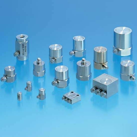 What is a Vibration Sensor?
24 October 20252950
 Working Principle and Characteristics of Zener diodes
20 October 202524036
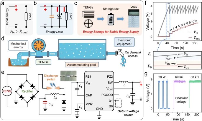 Improving the Energy Conversion Efficiency of Triboelectric Nanogenerators
19 November 20242545
Nexperia USA Inc.
In Stock: 22
Minimum: 1 Multiples: 1
Qty
Unit Price
Ext Price
1
$0.063677
$0.06
500
$0.046821
$23.41
1000
$0.039018
$39.02
2000
$0.035796
$71.59
5000
$0.033454
$167.27
10000
$0.031120
$311.20
15000
$0.030097
$451.46
50000
$0.029594
$1,479.70
Not the price you want? Send RFQ Now and we'll contact you ASAP.
Inquire for More Quantity
![74HCT86D,653]() 74HCT86D,653
74HCT86D,653Nexperia USA Inc.
![74HC04D,653]() 74HC04D,653
74HC04D,653Nexperia USA Inc.
![74HC32D,653]() 74HC32D,653
74HC32D,653Nexperia USA Inc.
![74AHC1G32GW,125]() 74AHC1G32GW,125
74AHC1G32GW,125Nexperia USA Inc.
![HEF4093BT,653]() HEF4093BT,653
HEF4093BT,653Nexperia USA Inc.
![74HC02D,653]() 74HC02D,653
74HC02D,653Nexperia USA Inc.
![74LVC14APW,118]() 74LVC14APW,118
74LVC14APW,118Nexperia USA Inc.
![74AUP1G08GX,125]() 74AUP1G08GX,125
74AUP1G08GX,125Nexperia USA Inc.
![74LVC1G14GV,125]() 74LVC1G14GV,125
74LVC1G14GV,125Nexperia USA Inc.
![HEF4069UBT,653]() HEF4069UBT,653
HEF4069UBT,653Nexperia USA Inc.


