
 Product
 Brand
Brand Articles
 Tools
Tools
IR2113 High And Low Side Driver: 1.2V, 500V IGBT Driver IC, 14 PDIP and Schematic

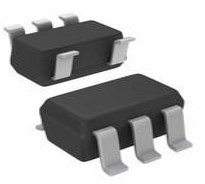
Through Hole Tube Active EAR99 Gate Drivers ICs Non-Inverting 14-DIP (0.300, 7.62mm) IR2113PBF
Unit Price: $2.042402
Ext Price: $2.04


Through Hole Tube Active EAR99 Gate Drivers ICs Non-Inverting 14-DIP (0.300, 7.62mm) IR2113PBF
The IR2113 is a high voltage, high-speed power MOSFET and IGBT driver with independent high and low side referenced output channels. This article will introduce detailed info about IR2113 driver ic.

IR2113
What is IR2113?
The IR2113 is a high voltage, high-speed power MOSFET and IGBT driver with independent high and low side referenced output channels. The output drivers feature a high pulse current buffer stage designed for minimum driver cross-conduction.
IR2113 Pinout

IR2113 Pinout
IR2113 CAD Model

IR2113 Symbol

IR2113 Footprint

IR2113 3D Model
Specifications
- TypeParameter
- Factory Lead Time12 Weeks
- Mount
In electronic components, the term "Mount" typically refers to the method or process of physically attaching or fixing a component onto a circuit board or other electronic device. This can involve soldering, adhesive bonding, or other techniques to secure the component in place. The mounting process is crucial for ensuring proper electrical connections and mechanical stability within the electronic system. Different components may have specific mounting requirements based on their size, shape, and function, and manufacturers provide guidelines for proper mounting procedures to ensure optimal performance and reliability of the electronic device.
Surface Mount, Through Hole - Mounting Type
The "Mounting Type" in electronic components refers to the method used to attach or connect a component to a circuit board or other substrate, such as through-hole, surface-mount, or panel mount.
Through Hole - Package / Case
refers to the protective housing that encases an electronic component, providing mechanical support, electrical connections, and thermal management.
14-DIP (0.300, 7.62mm) - Number of Pins14
- Driver ConfigurationHalf-Bridge
- Logic voltage-VIL, VIH6V 9.5V
- Turn Off Delay Time
It is the time from when Vgs drops below 90% of the gate drive voltage to when the drain current drops below 90% of the load current. It is the delay before current starts to transition in the load, and depends on Rg. Ciss.
20 ns - Operating Temperature
The operating temperature is the range of ambient temperature within which a power supply, or any other electrical equipment, operate in. This ranges from a minimum operating temperature, to a peak or maximum operating temperature, outside which, the power supply may fail.
-40°C~150°C TJ - Packaging
Semiconductor package is a carrier / shell used to contain and cover one or more semiconductor components or integrated circuits. The material of the shell can be metal, plastic, glass or ceramic.
Tube - Published1996
- Part Status
Parts can have many statuses as they progress through the configuration, analysis, review, and approval stages.
Active - Moisture Sensitivity Level (MSL)
Moisture Sensitivity Level (MSL) is a standardized rating that indicates the susceptibility of electronic components, particularly semiconductors, to moisture-induced damage during storage and the soldering process, defining the allowable exposure time to ambient conditions before they require special handling or baking to prevent failures
1 (Unlimited) - Number of Terminations14
- Termination
Termination in electronic components refers to the practice of matching the impedance of a circuit to prevent signal reflections and ensure maximum power transfer. It involves the use of resistors or other components at the end of transmission lines or connections. Proper termination is crucial in high-frequency applications to maintain signal integrity and reduce noise.
SMD/SMT - ECCN Code
An ECCN (Export Control Classification Number) is an alphanumeric code used by the U.S. Bureau of Industry and Security to identify and categorize electronic components and other dual-use items that may require an export license based on their technical characteristics and potential for military use.
EAR99 - TypeIntegrated Circuit (IC)
- Max Power Dissipation
The maximum power that the MOSFET can dissipate continuously under the specified thermal conditions.
1.25W - Voltage - Supply
Voltage - Supply refers to the range of voltage levels that an electronic component or circuit is designed to operate with. It indicates the minimum and maximum supply voltage that can be applied for the device to function properly. Providing supply voltages outside this range can lead to malfunction, damage, or reduced performance. This parameter is critical for ensuring compatibility between different components in a circuit.
3.3V~20V - Terminal Position
In electronic components, the term "Terminal Position" refers to the physical location of the connection points on the component where external electrical connections can be made. These connection points, known as terminals, are typically used to attach wires, leads, or other components to the main body of the electronic component. The terminal position is important for ensuring proper connectivity and functionality of the component within a circuit. It is often specified in technical datasheets or component specifications to help designers and engineers understand how to properly integrate the component into their circuit designs.
DUAL - Number of Functions1
- Supply Voltage
Supply voltage refers to the electrical potential difference provided to an electronic component or circuit. It is crucial for the proper operation of devices, as it powers their functions and determines performance characteristics. The supply voltage must be within specified limits to ensure reliability and prevent damage to components. Different electronic devices have specific supply voltage requirements, which can vary widely depending on their design and intended application.
15V - Base Part Number
The "Base Part Number" (BPN) in electronic components serves a similar purpose to the "Base Product Number." It refers to the primary identifier for a component that captures the essential characteristics shared by a group of similar components. The BPN provides a fundamental way to reference a family or series of components without specifying all the variations and specific details.
IR2113PBF - Number of Outputs2
- Output Voltage
Output voltage is a crucial parameter in electronic components that refers to the voltage level produced by the component as a result of its operation. It represents the electrical potential difference between the output terminal of the component and a reference point, typically ground. The output voltage is a key factor in determining the performance and functionality of the component, as it dictates the level of voltage that will be delivered to the connected circuit or load. It is often specified in datasheets and technical specifications to ensure compatibility and proper functioning within a given system.
20V - Max Output Current
The maximum current that can be supplied to the load.
2A - Operating Supply Voltage
The voltage level by which an electrical system is designated and to which certain operating characteristics of the system are related.
15V - Nominal Supply Current
Nominal current is the same as the rated current. It is the current drawn by the motor while delivering rated mechanical output at its shaft.
340μA - Power Dissipation
the process by which an electronic or electrical device produces heat (energy loss or waste) as an undesirable derivative of its primary action.
1.25W - Output Current
The rated output current is the maximum load current that a power supply can provide at a specified ambient temperature. A power supply can never provide more current that it's rated output current unless there is a fault, such as short circuit at the load.
2.5A - Max Supply Current
Max Supply Current refers to the maximum amount of electrical current that a component can draw from its power supply under normal operating conditions. It is a critical parameter that ensures the component operates reliably without exceeding its thermal limits or damaging internal circuitry. Exceeding this current can lead to overheating, performance degradation, or failure of the component. Understanding this parameter is essential for designing circuits that provide adequate power while avoiding overload situations.
340μA - Propagation Delay
the flight time of packets over the transmission link and is limited by the speed of light.
150 ns - Input Type
Input type in electronic components refers to the classification of the signal or data that a component can accept for processing or conversion. It indicates whether the input is analog, digital, or a specific format such as TTL or CMOS. Understanding input type is crucial for ensuring compatibility between different electronic devices and circuits, as it determines how signals are interpreted and interacted with.
Non-Inverting - Turn On Delay Time
Turn-on delay, td(on), is the time taken to charge the input capacitance of the device before drain current conduction can start.
20 ns - Max Output Voltage
The maximum output voltage refers to the dynamic area beyond which the output is saturated in the positive or negative direction, and is limited according to the load resistance value.
20V - Reference Voltage
A voltage reference is an electronic device that ideally produces a fixed (constant) voltage irrespective of the loading on the device, power supply variations, temperature changes, and the passage of time. Voltage references are used in power supplies, analog-to-digital converters, digital-to-analog converters, and other measurement and control systems. Voltage references vary widely in performance; a regulator for a computer power supply may only hold its value to within a few percent of the nominal value, whereas laboratory voltage standards have precisions and stability measured in parts per million.
600V - Rise Time
In electronics, when describing a voltage or current step function, rise time is the time taken by a signal to change from a specified low value to a specified high value.
35ns - Fall Time (Typ)
Fall Time (Typ) is a parameter used to describe the time it takes for a signal to transition from a high level to a low level in an electronic component, such as a transistor or an integrated circuit. It is typically measured in nanoseconds or microseconds and is an important characteristic that affects the performance of the component in digital circuits. A shorter fall time indicates faster switching speeds and can result in improved overall circuit performance, such as reduced power consumption and increased data transmission rates. Designers often consider the fall time specification when selecting components for their circuits to ensure proper functionality and efficiency.
25 ns - Min Output Voltage
Min Output Voltage refers to the lowest voltage level that an electronic component, such as a voltage regulator or power supply, can provide reliably under specified conditions. It indicates the minimum threshold required for proper operation of connected devices. Operating below this voltage may lead to device malfunction or failure to operate as intended.
10V - Rise / Fall Time (Typ)
The parameter "Rise / Fall Time (Typ)" in electronic components refers to the time it takes for a signal to transition from a specified low level to a specified high level (rise time) or from a high level to a low level (fall time). It is typically measured in nanoseconds or picoseconds and is an important characteristic in determining the speed and performance of a component, such as a transistor or integrated circuit. A shorter rise/fall time indicates faster signal switching and can impact the overall speed and efficiency of a circuit. Designers often consider this parameter when selecting components for high-speed applications to ensure proper signal integrity and timing.
25ns 17ns - Channel Type
In electronic components, the parameter "Channel Type" refers to the type of channel through which electrical signals or current flow within the component. This parameter is commonly associated with field-effect transistors (FETs) and other semiconductor devices. The channel type can be categorized as either N-channel or P-channel, depending on the polarity of the majority charge carriers (electrons or holes) that carry the current within the channel. N-channel devices have an electron-conducting channel, while P-channel devices have a hole-conducting channel. Understanding the channel type is crucial for proper circuit design and component selection to ensure compatibility and optimal performance.
Independent - Turn On Time
The time that it takes a gate circuit to allow a current to reach its full value.
0.15 μs - Output Peak Current Limit-Nom
Output Peak Current Limit-Nom is a parameter in electronic components that specifies the maximum current that can be delivered by the output under normal operating conditions. This limit is typically set to protect the component from damage due to excessive current flow. It ensures that the component operates within its safe operating limits and prevents overheating or other potential issues. Designers and engineers use this parameter to ensure proper functioning and reliability of the electronic system in which the component is used.
2.5A - Gate Type
In electronic components, the term "Gate Type" typically refers to the type of logic gate used in digital circuits. A logic gate is a fundamental building block of digital circuits that performs a specific logical operation based on the input signals it receives. Common types of logic gates include AND, OR, NOT, NAND, NOR, XOR, and XNOR gates.The Gate Type parameter specifies the specific logic function that the gate performs, such as AND, OR, or NOT. Different gate types have different truth tables that define their behavior based on the input signals. By selecting the appropriate gate type for a given application, designers can implement various logical functions and operations in digital circuits.Understanding the gate type is essential for designing and analyzing digital circuits, as it determines how the circuit processes and manipulates binary data. Choosing the right gate type is crucial for ensuring the correct functionality and performance of the digital system being designed.
IGBT, N-Channel MOSFET - Current - Peak Output (Source, Sink)
The parameter "Current - Peak Output (Source, Sink)" in electronic components refers to the maximum amount of current that the component can either supply (source) or sink (absorb) under peak conditions. This parameter is important for understanding the capability of the component to handle sudden surges or spikes in current without being damaged. The peak output current is typically specified in datasheets and is crucial for designing circuits that require high current handling capabilities. It is essential to consider this parameter to ensure the component operates within its safe operating limits and to prevent potential damage or malfunction.
2A 2A - High Side Driver
A High Side Driver is an electronic component used in power management applications to control the switching of high-side power devices such as MOSFETs or IGBTs. It is designed to drive the gate or base of the power device to turn it on or off, allowing current to flow through the load or cutting off the current flow. High Side Drivers are commonly used in automotive, industrial, and consumer electronics to control various loads such as motors, solenoids, and heaters. They provide isolation between the control circuitry and the high-side power device, ensuring safe and reliable operation of the system.
YES - Height2.35mm
- Length10.4902mm
- Width7.11mm
- REACH SVHC
The parameter "REACH SVHC" in electronic components refers to the compliance with the Registration, Evaluation, Authorization, and Restriction of Chemicals (REACH) regulation regarding Substances of Very High Concern (SVHC). SVHCs are substances that may have serious effects on human health or the environment, and their use is regulated under REACH to ensure their safe handling and minimize their impact.Manufacturers of electronic components need to declare if their products contain any SVHCs above a certain threshold concentration and provide information on the safe use of these substances. This information allows customers to make informed decisions about the potential risks associated with using the components and take appropriate measures to mitigate any hazards.Ensuring compliance with REACH SVHC requirements is essential for electronics manufacturers to meet regulatory standards, protect human health and the environment, and maintain transparency in their supply chain. It also demonstrates a commitment to sustainability and responsible manufacturing practices in the electronics industry.
No SVHC - Radiation Hardening
Radiation hardening is the process of making electronic components and circuits resistant to damage or malfunction caused by high levels of ionizing radiation, especially for environments in outer space (especially beyond the low Earth orbit), around nuclear reactors and particle accelerators, or during nuclear accidents or nuclear warfare.
No - RoHS Status
RoHS means “Restriction of Certain Hazardous Substances” in the “Hazardous Substances Directive” in electrical and electronic equipment.
ROHS3 Compliant - Lead Free
Lead Free is a term used to describe electronic components that do not contain lead as part of their composition. Lead is a toxic material that can have harmful effects on human health and the environment, so the electronics industry has been moving towards lead-free components to reduce these risks. Lead-free components are typically made using alternative materials such as silver, copper, and tin. Manufacturers must comply with regulations such as the Restriction of Hazardous Substances (RoHS) directive to ensure that their products are lead-free and environmentally friendly.
Contains Lead, Lead Free
IR2113 Features
Floating channel designed for bootstrap operation
Fully operational to +500V or +600V
Tolerant to negative transient voltage dV/dt immune
Gate drive supply range from 10 to 20V
Under-voltage lockout for both channels
3.3V logic compatible
Separate logic supply range from 3.3V to 20V
Logic and power ground ±5V offset
CMOS Schmitt-triggered inputs with pull-down
Cycle by cycle edge-triggered shutdown logic
Matched propagation delay for both channels
Outputs in phase with inputs
IR2113 Typical Connection
The following is the typical connection of IR2113

IR2113 Typical Connection
IR2113 Functional Block Diagram

IR2113 Functional Block Diagram
IR2113 Equivalents
IRF470, IR2110, IR1176, IRF450, IRF9460
IR2113 Package Outlines


IR2113 Package Outlines
IR2113 Manufacturer
On April 1st, 1999, Siemens Semiconductors became Infineon Technologies. A dynamic more flexible company geared towards success in the competitive, ever-changing world of microelectronics. Infineon is a leading global designer, manufacturer, and supplier of a broad range of semiconductors used in various microelectronic applications. Infineon's product portfolio consists of logic products, including digital, mixed-signal, and analog integrated circuits, as well as discrete semiconductor products.
Parts with Similar Specs
- ImagePart NumberManufacturerPackage / CaseNumber of PinsChannel TypeMax Output CurrentOutput CurrentRise TimeSupply VoltageMax Power DissipationView Compare
![IR2113PBF]()
IR2113PBF
14-DIP (0.300, 7.62mm)
14
Independent
2 A
2.5 A
35 ns
15 V
1.25 W
![FAN7392N]()
14-DIP (0.300, 7.62mm)
14
Independent
1.2 A
1.2 A
25 ns
-
1.5 W
![MIC4467ZN]()
14-DIP (0.300, 7.62mm)
14
Independent
3 A
3 A
25 ns
15 V
1.6 W
![MIC4469BN]()
14-DIP (0.300, 7.62mm)
14
Independent
1.2 A
1.2 A
25 ns
-
1.5 W
![MIC4469YN]()
14-DIP (0.300, 7.62mm)
-
Independent
-
-
-
-
-

Trend Analysis
Datasheet PDF
- PCN Packaging :
- Datasheets :
- Other Related Documents :
- ConflictMineralStatement :
What is the use of IR2113?
The IR2113 are high voltage, high-speed power MOSFET and IGBT drivers with independent high and low side referenced output channels. The floating channel can be used to drive an N-channel power MOSFET or IGBT in the high side configuration which operates up to 500 or 600 volts.
How does IR2113 work?
An IR2113 is a power amplifier that accepts a low-power input from a controller IC and produces the appropriate high current gate drive for a power device. To operate a MOSFET/IGBT, typically a voltage has to be applied to the gate that is relative to the source/emitter of the device.
What are the benefits of Gate Drive Control ICs?
The HVAC gate drive solution typically cuts down on component counts and PCB size by 50 percent compared to discrete solutions. These devices offer an improved immunity to voltage spikes and contribute to lower switching losses for the IGBTs and FETs. Fast switching times, under-voltage lockout protection, included dead time are other advantages of these drivers.
 TCA9555RTWR Low-Voltage I/O Expander: Features, Applications and datasheet
07 January 20221227
 MLX90640 Sensor: Datasheet, Pinout and Alternatives
26 August 202110540
 1N5822 Schottky Diode: Pinout, Datasheet, and Applications
12 July 20217019
 Never Struggle Again With Microchip PG164140 Issues
16 August 2025159
.png) AD558: A Versatile Digital to Analog Converter for Precise Voltage Output
AD558: A Versatile Digital to Analog Converter for Precise Voltage Output06 March 2024432
 Quadruple Half-H Driver - L293DNE:Datasheet, Pinout, Circuit and Specification
12 April 20226383
 TPS2051CDBVR Power-Distribution Switches: Layout, Pinout, and Datasheet
09 April 20221962
 AD9226 65 MSPS 12-bit ADC: High-Speed Data Acquisition and FPGA Integration Guide
14 March 2026358
 How do Solar Cells Work?
20 November 20203098
 Characteristics, Types, and Functions of Electrolytic Capacitors
17 October 202510405
 Introduction to PCB Layout Principles
13 November 20206910
 Apple M1 Ultra -- The Technology Behind the Chip Interconnection
12 March 20227046
 What is an LDO (Low Dropout Regulator)?
29 October 20216305
 Advanced Aircraft Power Electronics Systems and Influence of Simulation, Standards, and Wide Band-Gap Devices
18 February 20242890
 Why does a MOSFET with a Small Internal Resistance Heat Up?
09 May 20223863
 Top 10 Technology Trends in the Global Semiconductor Industry in 2022
08 January 20229251
Infineon Technologies
In Stock: 600
Minimum: 1 Multiples: 1
Qty
Unit Price
Ext Price
1
$2.042402
$2.04
10
$1.926795
$19.27
100
$1.817731
$181.77
500
$1.714840
$857.42
1000
$1.617774
$1,617.77
Not the price you want? Send RFQ Now and we'll contact you ASAP.
Inquire for More Quantity
![IR2110SPBF]() IR2110SPBF
IR2110SPBFInfineon Technologies
![IR2104SPBF]() IR2104SPBF
IR2104SPBFInfineon Technologies
![IR2184SPBF]() IR2184SPBF
IR2184SPBFInfineon Technologies
![IR2181SPBF]() IR2181SPBF
IR2181SPBFInfineon Technologies
![IR2183SPBF]() IR2183SPBF
IR2183SPBFInfineon Technologies
![IRS2113STRPBF]() IRS2113STRPBF
IRS2113STRPBFInfineon Technologies
![IR2153SPBF]() IR2153SPBF
IR2153SPBFInfineon Technologies
![IR2214SSPBF]() IR2214SSPBF
IR2214SSPBFInfineon Technologies
![IR2102SPBF]() IR2102SPBF
IR2102SPBFInfineon Technologies


