
 Product
 Brand
Brand Articles
 Tools
Tools
LM324 Quad OP-AMP IC[FAQ+Video]: Datasheet, LM324 vs LM358, and Pinout

4 Channels 40mA per Channel 40nA 65 dB Instrumentational OP Amps 5V 3V~32V ±1.5V~16V LM324 14-DIP (0.300, 7.62mm)


4 Channels 40mA per Channel 40nA 65 dB Instrumentational OP Amps 5V 3V~32V ±1.5V~16V LM324 14-DIP (0.300, 7.62mm)
LM324 is an operational amplifier consisting of four channels. Today, we will walk you into the introduction of the popular Quad op-amp LM324, you will learn its pinout, features, application, circuit diagram, and its differences with LM358 and more.

Top 5 LM324 ic diy electronics projects, 5 awesome electronics circuit
LM324 Overview
LM324 is a Quad op-amp IC integrated with four op-amps powered by a common power supply. The differential input voltage range can be equal to that of the power supply voltage. The default input offset voltage is very low which is of magnitude 2mV. The operating temperature ranges from 0˚C to 70˚C at ambient whereas the maximum junction temperature can be up to 150˚C. Generally, op-amps can perform mathematical operations.
LM324 Pinout and Configuration

| Pin Number | Pin Name | Description |
| 1 | OUTPUT1 | The output of Op-Amp 1 |
| 2 | INPUT1- | Inverting Input of Op-Amp 1 |
| 3 | INPUT1+ | Non-Inverting Input of Op-Amp 1 |
| 4 | VCC | Positive Supply Voltage |
| 5 | INPUT2+ | Non-Inverting Input of Op-Amp 2 |
| 6 | INPUT2- | Inverting Input of Op-Amp 2 |
| 7 | OUTPUT2 | The output of Op-Amp 2 |
| 8 | OUTPUT3 | The output of Op-Amp 3 |
| 9 | INPUT3- | Inverting Input of Op-Amp 3 |
| 10 | INPUT3+ | Non-Inverting Input of Op-Amp 3 |
| 11 | VEE, GND | Ground or Negative Supply Voltage |
| 12 | INPUT4+ | Non-Inverting Input of Op-Amp 4 |
| 13 | INPUT4- | Inverting Input of Op-Amp 4 |
| 14 | OUTPUT4 | The output of Op-Amp 4 |
Specifications
- TypeParameter
- Lifecycle Status
Lifecycle Status refers to the current stage of an electronic component in its product life cycle, indicating whether it is active, obsolete, or transitioning between these states. An active status means the component is in production and available for purchase. An obsolete status indicates that the component is no longer being manufactured or supported, and manufacturers typically provide a limited time frame for support. Understanding the lifecycle status is crucial for design engineers to ensure continuity and reliability in their projects.
LAST SHIPMENTS (Last Updated: 3 days ago) - Factory Lead Time7 Weeks
- Mount
In electronic components, the term "Mount" typically refers to the method or process of physically attaching or fixing a component onto a circuit board or other electronic device. This can involve soldering, adhesive bonding, or other techniques to secure the component in place. The mounting process is crucial for ensuring proper electrical connections and mechanical stability within the electronic system. Different components may have specific mounting requirements based on their size, shape, and function, and manufacturers provide guidelines for proper mounting procedures to ensure optimal performance and reliability of the electronic device.
Through Hole - Mounting Type
The "Mounting Type" in electronic components refers to the method used to attach or connect a component to a circuit board or other substrate, such as through-hole, surface-mount, or panel mount.
Through Hole - Package / Case
refers to the protective housing that encases an electronic component, providing mechanical support, electrical connections, and thermal management.
14-DIP (0.300, 7.62mm) - Number of Pins14
- Supplier Device Package
The parameter "Supplier Device Package" in electronic components refers to the physical packaging or housing of the component as provided by the supplier. It specifies the form factor, dimensions, and layout of the component, which are crucial for compatibility and integration into electronic circuits and systems. The supplier device package information typically includes details such as the package type (e.g., DIP, SOP, QFN), number of pins, pitch, and overall size, allowing engineers and designers to select the appropriate component for their specific application requirements. Understanding the supplier device package is essential for proper component selection, placement, and soldering during the manufacturing process to ensure optimal performance and reliability of the electronic system.
14-DIP - Weight1.62g
- Number of Elements4
- Operating Temperature
The operating temperature is the range of ambient temperature within which a power supply, or any other electrical equipment, operate in. This ranges from a minimum operating temperature, to a peak or maximum operating temperature, outside which, the power supply may fail.
0°C~70°C - Packaging
Semiconductor package is a carrier / shell used to contain and cover one or more semiconductor components or integrated circuits. The material of the shell can be metal, plastic, glass or ceramic.
Tube - Published2010
- Part Status
Parts can have many statuses as they progress through the configuration, analysis, review, and approval stages.
Obsolete - Moisture Sensitivity Level (MSL)
Moisture Sensitivity Level (MSL) is a standardized rating that indicates the susceptibility of electronic components, particularly semiconductors, to moisture-induced damage during storage and the soldering process, defining the allowable exposure time to ambient conditions before they require special handling or baking to prevent failures
1 (Unlimited) - Max Operating Temperature
The Maximum Operating Temperature is the maximum body temperature at which the thermistor is designed to operate for extended periods of time with acceptable stability of its electrical characteristics.
70°C - Min Operating Temperature
The "Min Operating Temperature" parameter in electronic components refers to the lowest temperature at which the component is designed to operate effectively and reliably. This parameter is crucial for ensuring the proper functioning and longevity of the component, as operating below this temperature may lead to performance issues or even damage. Manufacturers specify the minimum operating temperature to provide guidance to users on the environmental conditions in which the component can safely operate. It is important to adhere to this parameter to prevent malfunctions and ensure the overall reliability of the electronic system.
0°C - Max Power Dissipation
The maximum power that the MOSFET can dissipate continuously under the specified thermal conditions.
1.31W - Base Part Number
The "Base Part Number" (BPN) in electronic components serves a similar purpose to the "Base Product Number." It refers to the primary identifier for a component that captures the essential characteristics shared by a group of similar components. The BPN provides a fundamental way to reference a family or series of components without specifying all the variations and specific details.
LM324 - Operating Supply Voltage
The voltage level by which an electrical system is designated and to which certain operating characteristics of the system are related.
5V - Number of Channels4
- Number of Circuits4
- Max Supply Voltage
In general, the absolute maximum common-mode voltage is VEE-0.3V and VCC+0.3V, but for products without a protection element at the VCC side, voltages up to the absolute maximum rated supply voltage (i.e. VEE+36V) can be supplied, regardless of supply voltage.
32V - Min Supply Voltage
The minimum supply voltage (V min ) is explored for sequential logic circuits by statistically simulating the impact of within-die process variations and gate-dielectric soft breakdown on data retention and hold time.
3V - Operating Supply Current
Operating Supply Current, also known as supply current or quiescent current, is a crucial parameter in electronic components that indicates the amount of current required for the device to operate under normal conditions. It represents the current drawn by the component from the power supply while it is functioning. This parameter is important for determining the power consumption of the component and is typically specified in datasheets to help designers calculate the overall power requirements of their circuits. Understanding the operating supply current is essential for ensuring proper functionality and efficiency of electronic systems.
1mA - Nominal Supply Current
Nominal current is the same as the rated current. It is the current drawn by the motor while delivering rated mechanical output at its shaft.
1.2mA - Power Dissipation
the process by which an electronic or electrical device produces heat (energy loss or waste) as an undesirable derivative of its primary action.
1.31W - Output Current
The rated output current is the maximum load current that a power supply can provide at a specified ambient temperature. A power supply can never provide more current that it's rated output current unless there is a fault, such as short circuit at the load.
40mA - Max Supply Current
Max Supply Current refers to the maximum amount of electrical current that a component can draw from its power supply under normal operating conditions. It is a critical parameter that ensures the component operates reliably without exceeding its thermal limits or damaging internal circuitry. Exceeding this current can lead to overheating, performance degradation, or failure of the component. Understanding this parameter is essential for designing circuits that provide adequate power while avoiding overload situations.
700μA - Current - Supply
Current - Supply is a parameter in electronic components that refers to the maximum amount of electrical current that the component can provide to the circuit it is connected to. It is typically measured in units of amperes (A) and is crucial for determining the power handling capability of the component. Understanding the current supply rating is important for ensuring that the component can safely deliver the required current without overheating or failing. It is essential to consider this parameter when designing circuits to prevent damage to the component and ensure proper functionality of the overall system.
1mA - Slew Rate
the maximum rate of output voltage change per unit time.
0.3 V/μs - Amplifier Type
Amplifier Type refers to the classification or categorization of amplifiers based on their design, functionality, and characteristics. Amplifiers are electronic devices that increase the amplitude of a signal, such as voltage or current. The type of amplifier determines its specific application, performance capabilities, and operating characteristics. Common types of amplifiers include operational amplifiers (op-amps), power amplifiers, audio amplifiers, and radio frequency (RF) amplifiers. Understanding the amplifier type is crucial for selecting the right component for a particular circuit or system design.
General Purpose - Common Mode Rejection Ratio
Common Mode Rejection Ratio (CMRR) is a measure of the ability of a differential amplifier to reject input signals that are common to both input terminals. It is defined as the ratio of the differential gain to the common mode gain. A high CMRR indicates that the amplifier can effectively eliminate noise and interference that affects both inputs simultaneously, enhancing the fidelity of the amplified signal. CMRR is typically expressed in decibels (dB), with higher values representing better performance in rejecting common mode signals.
65 dB - Current - Input Bias
The parameter "Current - Input Bias" in electronic components refers to the amount of current required at the input terminal of a device to maintain proper operation. It is a crucial specification as it determines the minimum input current needed for the component to function correctly. Input bias current can affect the performance and accuracy of the device, especially in precision applications where small signal levels are involved. It is typically specified in datasheets for operational amplifiers, transistors, and other semiconductor devices to provide users with important information for circuit design and analysis.
40nA - Voltage - Supply, Single/Dual (±)
The parameter "Voltage - Supply, Single/Dual (±)" in electronic components refers to the power supply voltage required for the proper operation of the component. This parameter indicates whether the component requires a single power supply voltage (e.g., 5V) or a dual power supply voltage (e.g., ±15V). For components that require a single power supply voltage, only one voltage level is needed for operation. On the other hand, components that require a dual power supply voltage need both positive and negative voltage levels to function correctly.Understanding the voltage supply requirements of electronic components is crucial for designing and integrating them into circuits to ensure proper functionality and prevent damage due to incorrect voltage levels.
3V~32V ±1.5V~16V - Output Current per Channel
Output Current per Channel is a specification commonly found in electronic components such as amplifiers, audio interfaces, and power supplies. It refers to the maximum amount of electrical current that can be delivered by each individual output channel of the component. This parameter is important because it determines the capacity of the component to drive connected devices or loads. A higher output current per channel means the component can deliver more power to connected devices, while a lower output current may limit the performance or functionality of the component in certain applications. It is crucial to consider the output current per channel when selecting electronic components to ensure they can meet the power requirements of the intended system or setup.
40mA - Input Offset Voltage (Vos)
Input Offset Voltage (Vos) is a key parameter in electronic components, particularly in operational amplifiers. It refers to the voltage difference that must be applied between the two input terminals of the amplifier to nullify the output voltage when the input terminals are shorted together. In simpler terms, it represents the voltage required to bring the output of the amplifier to zero when there is no input signal present. Vos is an important parameter as it can introduce errors in the output signal of the amplifier, especially in precision applications where accuracy is crucial. Minimizing Vos is essential to ensure the amplifier operates with high precision and accuracy.
7mV - Bandwidth
In electronic components, "Bandwidth" refers to the range of frequencies over which the component can effectively operate or pass signals without significant loss or distortion. It is a crucial parameter for devices like amplifiers, filters, and communication systems. The bandwidth is typically defined as the difference between the upper and lower frequencies at which the component's performance meets specified criteria, such as a certain level of signal attenuation or distortion. A wider bandwidth indicates that the component can handle a broader range of frequencies, making it more versatile for various applications. Understanding the bandwidth of electronic components is essential for designing and optimizing circuits to ensure proper signal transmission and reception within the desired frequency range.
12 kHz - Gain Bandwidth Product
The gain–bandwidth product (designated as GBWP, GBW, GBP, or GB) for an amplifier is the product of the amplifier's bandwidth and the gain at which the bandwidth is measured.
1MHz - Voltage Gain
Voltage gain is a measure of how much an electronic component or circuit amplifies an input voltage signal to produce an output voltage signal. It is typically expressed as a ratio or in decibels (dB). A higher voltage gain indicates a greater amplification of the input signal. Voltage gain is an important parameter in amplifiers, where it determines the level of amplification provided by the circuit. It is calculated by dividing the output voltage by the input voltage and is a key factor in determining the overall performance and functionality of electronic devices.
100dB - Power Supply Rejection Ratio (PSRR)
Power Supply Rejection Ratio (PSRR) is a measure of how well an electronic component, such as an operational amplifier or voltage regulator, can reject changes in its supply voltage. It indicates the ability of the component to maintain a stable output voltage despite fluctuations in the input supply voltage. A higher PSRR value signifies better performance in rejecting noise and variations from the power supply, leading to improved signal integrity and more reliable operation in electronic circuits. PSRR is typically expressed in decibels (dB).
65dB - Voltage - Input Offset
Voltage - Input Offset is a parameter that refers to the difference in voltage between the input terminals of an electronic component, such as an operational amplifier, when the input voltage is zero. It is an important characteristic that can affect the accuracy and performance of the component in various applications. A low input offset voltage is desirable as it indicates that the component will have minimal error in its output when the input signal is near zero. Manufacturers typically provide this specification in the component's datasheet to help users understand the component's behavior and make informed decisions when designing circuits.
1.5mV - Gain
In electronic components, "Gain" refers to the ratio of the output signal amplitude to the input signal amplitude. It is a measure of the amplification provided by the component, such as a transistor or operational amplifier. Gain is typically expressed in decibels (dB) or as a numerical value, indicating how much the signal is amplified by the component.A higher gain value indicates a greater amplification of the input signal, while a lower gain value indicates less amplification. Gain is an important parameter in designing and analyzing electronic circuits, as it determines the overall performance and functionality of the system. Different components have different gain characteristics, and understanding the gain of a component is crucial for achieving the desired signal processing or amplification in electronic systems.
100 dB - Max Dual Supply Voltage
A Dual power supply is a regular direct current power supply. It can provide a positive as well as negative voltage. It ensures stable power supply to the device as well as it helps to prevent system damage.
16V - Max Frequency
Max Frequency refers to the highest frequency at which an electronic component can operate effectively without degradation of performance. It is a critical parameter for devices such as transistors, capacitors, and oscillators, indicating their limitations in speed and response time. Exceeding the max frequency can lead to issues like signal distortion, heat generation, and potential failure of the component. Understanding this parameter is essential for designing circuits to ensure reliable and efficient operation.
20kHz - Min Dual Supply Voltage
The parameter "Min Dual Supply Voltage" in electronic components refers to the minimum voltage required for the proper operation of a device that uses dual power supplies. Dual power supplies typically consist of a positive and a negative voltage source. The "Min Dual Supply Voltage" specification ensures that both the positive and negative supply voltages are within a certain range to guarantee the device functions correctly. It is important to adhere to this parameter to prevent damage to the component and ensure reliable performance.
1.5V - Dual Supply Voltage
Dual Supply Voltage refers to an electronic component's requirement for two separate power supply voltages, typically one positive and one negative. This configuration is commonly used in operational amplifiers, analog circuits, and certain digital devices to allow for greater signal handling capabilities and improved performance. The use of dual supply voltages enables the device to process bipolar signals, thereby enhancing its functionality in various applications.
3V - Number of Amplifiers4
- Height3.25mm
- Length19.3mm
- Width6.35mm
- REACH SVHC
The parameter "REACH SVHC" in electronic components refers to the compliance with the Registration, Evaluation, Authorization, and Restriction of Chemicals (REACH) regulation regarding Substances of Very High Concern (SVHC). SVHCs are substances that may have serious effects on human health or the environment, and their use is regulated under REACH to ensure their safe handling and minimize their impact.Manufacturers of electronic components need to declare if their products contain any SVHCs above a certain threshold concentration and provide information on the safe use of these substances. This information allows customers to make informed decisions about the potential risks associated with using the components and take appropriate measures to mitigate any hazards.Ensuring compliance with REACH SVHC requirements is essential for electronics manufacturers to meet regulatory standards, protect human health and the environment, and maintain transparency in their supply chain. It also demonstrates a commitment to sustainability and responsible manufacturing practices in the electronics industry.
No SVHC - Radiation Hardening
Radiation hardening is the process of making electronic components and circuits resistant to damage or malfunction caused by high levels of ionizing radiation, especially for environments in outer space (especially beyond the low Earth orbit), around nuclear reactors and particle accelerators, or during nuclear accidents or nuclear warfare.
No - RoHS Status
RoHS means “Restriction of Certain Hazardous Substances” in the “Hazardous Substances Directive” in electrical and electronic equipment.
RoHS Compliant - Lead Free
Lead Free is a term used to describe electronic components that do not contain lead as part of their composition. Lead is a toxic material that can have harmful effects on human health and the environment, so the electronics industry has been moving towards lead-free components to reduce these risks. Lead-free components are typically made using alternative materials such as silver, copper, and tin. Manufacturers must comply with regulations such as the Restriction of Hazardous Substances (RoHS) directive to ensure that their products are lead-free and environmentally friendly.
Lead Free
What is Operational Amplifier
Operational amplifiers are simple electronic circuits that can boost a weak signal to a level of higher amplitude. An operational amplifier is generally used in applications such as home entertainment systems, megaphones, speakers, microphones, etc. An op-amp usually operates with a number of feedback components that determine the resulting function or “operation” of the amplifier and by virtue of the different feedback, configurations whether resistive, capacitive, or both.
LM324 Features
Wide supply ranges
Single supply: 3 V to 32 V
Dual supplies: ±1.5 V to ±16 V
Low supply current drain independent of supply voltage: 0.8 mA typical
Common-mode input voltage range includes ground, allowing direct sensing near the ground
Differential input voltage range equal to maximum-rated supply voltage: 32 V
2 kV ESD protection
Low input bias and offset parameters
Input offset voltage: 3mV typical
Aversions: 2mV typical
Input offset current: 2 nA typical
Input bias current: 20 nA typical
Aversions: 15nA typical
Open-loop differential voltage amplification: 100 V/mV typical
Internal frequency compensation
LM324 Applications
Transducer Amplifiers
Filter circuits, Voltage followers
Integrator, Differentiator, Summer, adder, Voltage follower, etc.,
DC gain blocks
Comparators (Loop control & regulation)
LM324 Manufacturer
onsemi (legally ON Semiconductor Corporation; formerly ON Semiconductor until August 5, 2021) is an American semiconductor supplier company, formerly in the Fortune 500, but dropping into the Fortune 1000 (ranked 512) in 2020. Products include power and signal management, logic, discrete, and custom devices for automotive, communications, computing, consumer, industrial, LED lighting, medical, military/aerospace, and power applications. onsemi runs a network of manufacturing facilities, sales offices, and design centers in North America, Europe, and the Asia Pacific regions. Headquartered in Phoenix, Arizona, onsemi has revenues of $3.907 billion (2016), which puts it among the worldwide top 20 semiconductor sales leaders.
LM324 Package
Where and How to Use LM324?
LM324 can be operated by a single power source. Two power supplies can also be used. The terminals or the pins used are pins ④ and ⑪. This single supply or two power supplies will make all four OP-AMPs operative.
For the 1st OP-AMP, inverting input is applied at pin ② and non-inverting at pin ③. The output of the first OP-AMP is obtained at pin ①.
For the 2nd OP-AMP, inverting input is applied at pin ⑥ and non-inverting at pin ⑤. The output of the second OP-AMP is obtained at pin ⑦.
For the 3rd OP-AMP, inverting input is applied at pin ⑨ and non-inverting at pin ⑩. The output of the third OP-AMP is obtained at pin ⑧.
For the 4th OP-AMP, inverting input is applied at pin ⑬ and non-inverting at pin ⑫. The output of the fourth OP-AMP is obtained at pin ⑭.
LM324 vs LM358

LM324 vs LM358: specifications
| Specification | LM358 | LM324 |
| Supply voltage | 32V | 32V |
| Power dissipation | 830mW (DIP) | 1130mW (DIP) |
| Input offset voltage | 5mV | 5mV |
| Input offset voltage drift | 20µV/C (max.) | 30µV/C (max.) |
The only major differences in the specification have to do with power dissipation – the LM358 comes in a DIP-8 package, which is smaller than the DIP-14 package that the LM324 comes in. This means that the LM324 can dissipate more power than the LM358. This might also be the cause for the larger drift in offset voltage for the LM324.
LM324 vs LM358: inside circuitry

Taking a look at the internal circuit diagram, it is clear that both parts essentially have the same schematic for all amplifiers. Hence, the only possibility for errors arises from small differences in the way the semiconductors are manufactured and packaged.
Trend Analysis
Datasheet PDF
- PCN Obsolescence/ EOL :
- Datasheets :
- Environmental Information :
- PCN Assembly/Origin :
- PCN Design/Specification :
- PCN Packaging :
Parts with Similar Specs
- ImagePart NumberManufacturerPackage / CaseNumber of PinsNumber of CircuitsSlew RateGain Bandwidth ProductInput Offset Voltage (Vos)Power Supply Rejection Ratio (PSRR)Common Mode Rejection RatioMin Dual Supply VoltageMin Supply VoltageMax Dual Supply VoltageMax Supply VoltageView Compare
![LM324N]()
LM324N
14-DIP (0.300, 7.62mm)
14
4
0.3 V/μs
1 MHz
7 mV
65 dB
65 dB
1.5 V
3 V
16 V
32 V
![LM224N]()
14-DIP (0.300, 7.62mm)
14
-
0.4V/μs
-
7 mV
-
70 dB
-
-
-
-
![LM2902N]()
14-DIP (0.300, 7.62mm)
14
4
0.6 V/μs
1 MHz
7 mV
50 dB
50 dB
1.5 V
3 V
13 V
26 V
![LM2902N]()
14-DIP (0.300, 7.62mm)
14
4
0.5 V/μs
1 MHz
3 mV
65 dB
65 dB
1.5 V
3 V
16 V
32 V
![LM324AN]()
DIP
14
4
0.6 V/μs
1 MHz
5 mV
65 dB
70 dB
1.5 V
3 V
16 V
32 V


What is lm324?
LM324 is a Quad op-amp IC integrated with four op-amps powered by a common power supply. The differential input voltage range can be equal to that of the power supply voltage. ... Generally, op-amps can perform mathematical operations.
What is lm324 used for?
The applications of IC LM324 include the following. By using this IC, the conventional op-amp applications can be implemented very simply. This IC can be used as oscillators, rectifiers, amplifiers, comparators, etc.
What’s the differences between lm324 and lm358?
For all intents and purposes, the amplifiers inside the LM358 and LM324 are the same, the only difference between the two is the number of amplifiers per package and the power dissipation capability.
What’s lm324 recommended operation temperature?
It's between 0 and 70℃.
What’s lm324 number of channel?
4
 AD9364BBCZ RF Transceiver ICs: Package,Datasheet,Specification
14 May 20212427
 ATMEGA8-16PU 8-bit Microcontroller: Circuit, Pinout, and Datasheet
11 February 202210993
 CSD18540Q5B, Pinout, Package
21 March 20221710
![MJE13001 BJT NPN switching transistor[Video]](https://res.utmel.com/Images/Article/0502d4b7-5d95-45de-9fef-a1b0400767a2.png) MJE13001 BJT NPN switching transistor[Video]
MJE13001 BJT NPN switching transistor[Video]05 May 20221987
 KSZ9893R Gigabit Ethernet Switch: Pinout, Equivalent and Datasheet
17 February 20223146
 The Rj9 VS Rj11 Connectors-Who is the winner?
26 March 202218366
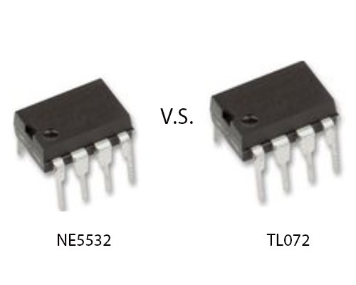 NE5532 Vs. TL072: What Is The Difference?
08 March 202224861
![L9110S 2-Channel Motor driver: Circuit, Pinout, and How to work [Video&FAQ]](https://res.utmel.com/Images/Article/085c82a8-d35a-437e-b4ec-b80c4165ea2c.png) L9110S 2-Channel Motor driver: Circuit, Pinout, and How to work [Video&FAQ]
L9110S 2-Channel Motor driver: Circuit, Pinout, and How to work [Video&FAQ]25 April 202221052
 SEMI: Semiconductor Materials Market to Exceed US$70 Billion By 2023
27 September 20222591
 Analysis of Common Misunderstandings of Isolation Technology
25 April 20225405
 Stepper Motor: Types, Working and Applications
26 December 202510059
 Ten Smart Sensor Technology Trends for IoT Applications
20 November 20216220
 Characteristics and Working Principle of IGBT
31 October 202521563
 Clock&Timing - Application Specific: A Dedicated Chip That Helps Produce Signals on the Circuit Board
22 February 20232078
 Characteristics, Types, and Functions of Electrolytic Capacitors
17 October 20259791
 Types and Application of Position Sensors
31 October 20256609
ON Semiconductor
In Stock: 98
United States
China
Canada
Japan
Russia
Germany
United Kingdom
Singapore
Italy
Hong Kong(China)
Taiwan(China)
France
Korea
Mexico
Netherlands
Malaysia
Austria
Spain
Switzerland
Poland
Thailand
Vietnam
India
United Arab Emirates
Afghanistan
Åland Islands
Albania
Algeria
American Samoa
Andorra
Angola
Anguilla
Antigua & Barbuda
Argentina
Armenia
Aruba
Australia
Azerbaijan
Bahamas
Bahrain
Bangladesh
Barbados
Belarus
Belgium
Belize
Benin
Bermuda
Bhutan
Bolivia
Bonaire, Sint Eustatius and Saba
Bosnia & Herzegovina
Botswana
Brazil
British Indian Ocean Territory
British Virgin Islands
Brunei
Bulgaria
Burkina Faso
Burundi
Cabo Verde
Cambodia
Cameroon
Cayman Islands
Central African Republic
Chad
Chile
Christmas Island
Cocos (Keeling) Islands
Colombia
Comoros
Congo
Congo (DRC)
Cook Islands
Costa Rica
Côte d’Ivoire
Croatia
Cuba
Curaçao
Cyprus
Czechia
Denmark
Djibouti
Dominica
Dominican Republic
Ecuador
Egypt
El Salvador
Equatorial Guinea
Eritrea
Estonia
Eswatini
Ethiopia
Falkland Islands
Faroe Islands
Fiji
Finland
French Guiana
French Polynesia
Gabon
Gambia
Georgia
Ghana
Gibraltar
Greece
Greenland
Grenada
Guadeloupe
Guam
Guatemala
Guernsey
Guinea
Guinea-Bissau
Guyana
Haiti
Honduras
Hungary
Iceland
Indonesia
Iran
Iraq
Ireland
Isle of Man
Israel
Jamaica
Jersey
Jordan
Kazakhstan
Kenya
Kiribati
Kosovo
Kuwait
Kyrgyzstan
Laos
Latvia
Lebanon
Lesotho
Liberia
Libya
Liechtenstein
Lithuania
Luxembourg
Macao(China)
Madagascar
Malawi
Maldives
Mali
Malta
Marshall Islands
Martinique
Mauritania
Mauritius
Mayotte
Micronesia
Moldova
Monaco
Mongolia
Montenegro
Montserrat
Morocco
Mozambique
Myanmar
Namibia
Nauru
Nepal
New Caledonia
New Zealand
Nicaragua
Niger
Nigeria
Niue
Norfolk Island
North Korea
North Macedonia
Northern Mariana Islands
Norway
Oman
Pakistan
Palau
Palestinian Authority
Panama
Papua New Guinea
Paraguay
Peru
Philippines
Pitcairn Islands
Portugal
Puerto Rico
Qatar
Réunion
Romania
Rwanda
Samoa
San Marino
São Tomé & Príncipe
Saudi Arabia
Senegal
Serbia
Seychelles
Sierra Leone
Sint Maarten
Slovakia
Slovenia
Solomon Islands
Somalia
South Africa
South Sudan
Sri Lanka
St Helena, Ascension, Tristan da Cunha
St. Barthélemy
St. Kitts & Nevis
St. Lucia
St. Martin
St. Pierre & Miquelon
St. Vincent & Grenadines
Sudan
Suriname
Svalbard & Jan Mayen
Sweden
Syria
Tajikistan
Tanzania
Timor-Leste
Togo
Tokelau
Tonga
Trinidad & Tobago
Tunisia
Turkey
Turkmenistan
Turks & Caicos Islands
Tuvalu
U.S. Outlying Islands
U.S. Virgin Islands
Uganda
Ukraine
Uruguay
Uzbekistan
Vanuatu
Vatican City
Venezuela
Wallis & Futuna
Yemen
Zambia
Zimbabwe
![LM301AN]() LM301AN
LM301ANON Semiconductor
![MC1458D]() MC1458D
MC1458DON Semiconductor
![LM2904DR2G]() LM2904DR2G
LM2904DR2GON Semiconductor
![LM358DR2G]() LM358DR2G
LM358DR2GON Semiconductor
![LM258DR2G]() LM258DR2G
LM258DR2GON Semiconductor
![LM324DR2G]() LM324DR2G
LM324DR2GON Semiconductor
![MC33078DR2G]() MC33078DR2G
MC33078DR2GON Semiconductor
![NCV2904DR2G]() NCV2904DR2G
NCV2904DR2GON Semiconductor
![NCV33072DR2G]() NCV33072DR2G
NCV33072DR2GON Semiconductor
![LM358DMR2G]() LM358DMR2G
LM358DMR2GON Semiconductor


