
 Product
 Brand
Brand Articles
 Tools
Tools
LM358 Dual Op-Amp: Pinout, Equivalent and Datasheet

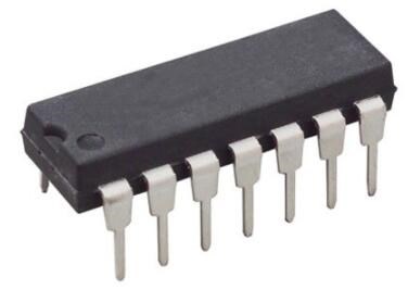
2 Channels 40mA per Channel 45nA 65 dB Instrumentational OP Amps 0.5μA 16V 3V~32V ±1.5V~16V LM358 8 Pins 8-SOIC (0.154, 3.90mm Width)


2 Channels 40mA per Channel 45nA 65 dB Instrumentational OP Amps 0.5μA 16V 3V~32V ±1.5V~16V LM358 8 Pins 8-SOIC (0.154, 3.90mm Width)
LM358 is a dual op-amp IC integrated with two op-amps powered by a common power supply. It can be considered as one half of LM324 Quad op-amp which contains four op-amps with common power supply. The LM358 series consists of two independent, high gain, internally frequency compensated operational amplifiers which were designed specifically to operate from a single power supply over a wide range of voltages. Furthermore, Huge range of Semiconductors, Capacitors, Resistors and IcS in stock. Welcome RFQ.

TOP 5 Electronics Projects using LM358 | OP-AMP
LM358 Pinout

Pinout
LM358 CAD Model

PCB Symbol

PCB Footprint

3D Model
LM358 Overview
Utilizing the circuit designs perfected for Quad Operational Amplifiers, these dual operational amplifiers feature low power drain, a common mode input voltage range extending to ground/VEE, and single supply or split supply operation. The LM358 series is equivalent to one−half of an LM324. These amplifiers have several distinct advantages over standard operational amplifier types in single supply applications. They can operate at supply voltages as low as 3.0 V or as high as 32 V, with quiescent currents about one−fifth of those associated with the MC1741 (on a per amplifier basis). The common mode input range includes the negative supply, thereby eliminating the necessity for external biasing components in many applications. The output voltage range also includes the negative power supply voltage.
This article provides you with a basic overview of the LM358 Dual Op-Amp, including its pin descriptions, features and specifications, etc., to help you quickly understand what LM358 is.
LM358 Features
● Short Circuit Protected Outputs
● True Differential Input Stage
● Single Supply Operation: 3.0 V to 32 V
● Low Input Bias Currents
● Internally Compensated
● Common Mode Range Extends to Negative Supply
● Single and Split Supply Operation
● ESD Clamps on the Inputs Increase Ruggedness of the Device without Affecting Operation
● Pb−Free Package May be Available. The G−Suffix Denotes a Pb−Free Lead Finish
Specifications
- TypeParameter
- Lifecycle Status
Lifecycle Status refers to the current stage of an electronic component in its product life cycle, indicating whether it is active, obsolete, or transitioning between these states. An active status means the component is in production and available for purchase. An obsolete status indicates that the component is no longer being manufactured or supported, and manufacturers typically provide a limited time frame for support. Understanding the lifecycle status is crucial for design engineers to ensure continuity and reliability in their projects.
LAST SHIPMENTS (Last Updated: 4 days ago) - Factory Lead Time11 Weeks
- Mounting Type
The "Mounting Type" in electronic components refers to the method used to attach or connect a component to a circuit board or other substrate, such as through-hole, surface-mount, or panel mount.
Surface Mount - Package / Case
refers to the protective housing that encases an electronic component, providing mechanical support, electrical connections, and thermal management.
8-SOIC (0.154, 3.90mm Width) - Surface Mount
having leads that are designed to be soldered on the side of a circuit board that the body of the component is mounted on.
YES - Number of Pins8
- Operating Temperature
The operating temperature is the range of ambient temperature within which a power supply, or any other electrical equipment, operate in. This ranges from a minimum operating temperature, to a peak or maximum operating temperature, outside which, the power supply may fail.
0°C~70°C - Packaging
Semiconductor package is a carrier / shell used to contain and cover one or more semiconductor components or integrated circuits. The material of the shell can be metal, plastic, glass or ceramic.
Tube - Published2005
- JESD-609 Code
The "JESD-609 Code" in electronic components refers to a standardized marking code that indicates the lead-free solder composition and finish of electronic components for compliance with environmental regulations.
e3 - Pbfree Code
The "Pbfree Code" parameter in electronic components refers to the code or marking used to indicate that the component is lead-free. Lead (Pb) is a toxic substance that has been widely used in electronic components for many years, but due to environmental concerns, there has been a shift towards lead-free alternatives. The Pbfree Code helps manufacturers and users easily identify components that do not contain lead, ensuring compliance with regulations and promoting environmentally friendly practices. It is important to pay attention to the Pbfree Code when selecting electronic components to ensure they meet the necessary requirements for lead-free applications.
yes - Part Status
Parts can have many statuses as they progress through the configuration, analysis, review, and approval stages.
Obsolete - Moisture Sensitivity Level (MSL)
Moisture Sensitivity Level (MSL) is a standardized rating that indicates the susceptibility of electronic components, particularly semiconductors, to moisture-induced damage during storage and the soldering process, defining the allowable exposure time to ambient conditions before they require special handling or baking to prevent failures
1 (Unlimited) - Number of Terminations8
- ECCN Code
An ECCN (Export Control Classification Number) is an alphanumeric code used by the U.S. Bureau of Industry and Security to identify and categorize electronic components and other dual-use items that may require an export license based on their technical characteristics and potential for military use.
EAR99 - Terminal Finish
Terminal Finish refers to the surface treatment applied to the terminals or leads of electronic components to enhance their performance and longevity. It can improve solderability, corrosion resistance, and overall reliability of the connection in electronic assemblies. Common finishes include nickel, gold, and tin, each possessing distinct properties suitable for various applications. The choice of terminal finish can significantly impact the durability and effectiveness of electronic devices.
Tin (Sn) - Packing Method
The packing method in electronic components refers to the technique used to package and protect the component during shipping and handling. It encompasses various forms including tape and reel, tray, tube, or bulk packaging, each suited for different types of components and manufacturing processes. The choice of packing method can affect the ease of handling, storage, and the efficiency of assembly in automated processes. Additionally, it plays a crucial role in ensuring the reliability and integrity of the components until they are used in electronic devices.
RAIL - Terminal Position
In electronic components, the term "Terminal Position" refers to the physical location of the connection points on the component where external electrical connections can be made. These connection points, known as terminals, are typically used to attach wires, leads, or other components to the main body of the electronic component. The terminal position is important for ensuring proper connectivity and functionality of the component within a circuit. It is often specified in technical datasheets or component specifications to help designers and engineers understand how to properly integrate the component into their circuit designs.
DUAL - Terminal Form
Occurring at or forming the end of a series, succession, or the like; closing; concluding.
GULL WING - Peak Reflow Temperature (Cel)
Peak Reflow Temperature (Cel) is a parameter that specifies the maximum temperature at which an electronic component can be exposed during the reflow soldering process. Reflow soldering is a common method used to attach electronic components to a circuit board. The Peak Reflow Temperature is crucial because it ensures that the component is not damaged or degraded during the soldering process. Exceeding the specified Peak Reflow Temperature can lead to issues such as component failure, reduced performance, or even permanent damage to the component. It is important for manufacturers and assemblers to adhere to the recommended Peak Reflow Temperature to ensure the reliability and functionality of the electronic components.
260 - Number of Functions2
- Supply Voltage
Supply voltage refers to the electrical potential difference provided to an electronic component or circuit. It is crucial for the proper operation of devices, as it powers their functions and determines performance characteristics. The supply voltage must be within specified limits to ensure reliability and prevent damage to components. Different electronic devices have specific supply voltage requirements, which can vary widely depending on their design and intended application.
5V - Time@Peak Reflow Temperature-Max (s)
Time@Peak Reflow Temperature-Max (s) refers to the maximum duration that an electronic component can be exposed to the peak reflow temperature during the soldering process, which is crucial for ensuring reliable solder joint formation without damaging the component.
40 - Base Part Number
The "Base Part Number" (BPN) in electronic components serves a similar purpose to the "Base Product Number." It refers to the primary identifier for a component that captures the essential characteristics shared by a group of similar components. The BPN provides a fundamental way to reference a family or series of components without specifying all the variations and specific details.
LM358 - Pin Count
a count of all of the component leads (or pins)
8 - Operating Supply Voltage
The voltage level by which an electrical system is designated and to which certain operating characteristics of the system are related.
16V - Power Supplies
an electronic circuit that converts the voltage of an alternating current (AC) into a direct current (DC) voltage.?
+-1.5/+-15/3/30V - Number of Channels2
- Operating Supply Current
Operating Supply Current, also known as supply current or quiescent current, is a crucial parameter in electronic components that indicates the amount of current required for the device to operate under normal conditions. It represents the current drawn by the component from the power supply while it is functioning. This parameter is important for determining the power consumption of the component and is typically specified in datasheets to help designers calculate the overall power requirements of their circuits. Understanding the operating supply current is essential for ensuring proper functionality and efficiency of electronic systems.
1.5mA - Nominal Supply Current
Nominal current is the same as the rated current. It is the current drawn by the motor while delivering rated mechanical output at its shaft.
1.2mA - Output Current
The rated output current is the maximum load current that a power supply can provide at a specified ambient temperature. A power supply can never provide more current that it's rated output current unless there is a fault, such as short circuit at the load.
40mA - Slew Rate
the maximum rate of output voltage change per unit time.
0.6V/μs - Architecture
In electronic components, the parameter "Architecture" refers to the overall design and structure of the component. It encompasses the arrangement of internal components, the layout of circuitry, and the physical form of the component. The architecture of an electronic component plays a crucial role in determining its functionality, performance, and compatibility with other components in a system. Different architectures can result in variations in power consumption, speed, size, and other key characteristics of the component. Designers often consider the architecture of electronic components carefully to ensure optimal performance and integration within a larger system.
VOLTAGE-FEEDBACK - Amplifier Type
Amplifier Type refers to the classification or categorization of amplifiers based on their design, functionality, and characteristics. Amplifiers are electronic devices that increase the amplitude of a signal, such as voltage or current. The type of amplifier determines its specific application, performance capabilities, and operating characteristics. Common types of amplifiers include operational amplifiers (op-amps), power amplifiers, audio amplifiers, and radio frequency (RF) amplifiers. Understanding the amplifier type is crucial for selecting the right component for a particular circuit or system design.
General Purpose - Common Mode Rejection Ratio
Common Mode Rejection Ratio (CMRR) is a measure of the ability of a differential amplifier to reject input signals that are common to both input terminals. It is defined as the ratio of the differential gain to the common mode gain. A high CMRR indicates that the amplifier can effectively eliminate noise and interference that affects both inputs simultaneously, enhancing the fidelity of the amplified signal. CMRR is typically expressed in decibels (dB), with higher values representing better performance in rejecting common mode signals.
65 dB - Current - Input Bias
The parameter "Current - Input Bias" in electronic components refers to the amount of current required at the input terminal of a device to maintain proper operation. It is a crucial specification as it determines the minimum input current needed for the component to function correctly. Input bias current can affect the performance and accuracy of the device, especially in precision applications where small signal levels are involved. It is typically specified in datasheets for operational amplifiers, transistors, and other semiconductor devices to provide users with important information for circuit design and analysis.
45nA - Voltage - Supply, Single/Dual (±)
The parameter "Voltage - Supply, Single/Dual (±)" in electronic components refers to the power supply voltage required for the proper operation of the component. This parameter indicates whether the component requires a single power supply voltage (e.g., 5V) or a dual power supply voltage (e.g., ±15V). For components that require a single power supply voltage, only one voltage level is needed for operation. On the other hand, components that require a dual power supply voltage need both positive and negative voltage levels to function correctly.Understanding the voltage supply requirements of electronic components is crucial for designing and integrating them into circuits to ensure proper functionality and prevent damage due to incorrect voltage levels.
3V~32V ±1.5V~16V - Halogen Free
The term "Halogen Free" in electronic components refers to a specific characteristic of the materials used in the manufacturing of the component. Halogens are a group of elements that include fluorine, chlorine, bromine, iodine, and astatine. These elements are commonly used in flame retardants and other materials in electronics. However, the presence of halogens can pose environmental and health risks when the components are disposed of or recycled.Therefore, electronic components labeled as "Halogen Free" are manufactured without the use of halogenated materials. This designation indicates that the components do not contain any halogens, making them safer for the environment and human health. Halogen-free components are becoming increasingly popular in the electronics industry due to the growing awareness of environmental concerns and regulations regarding hazardous substances in electronic products.
Halogen Free - Output Current per Channel
Output Current per Channel is a specification commonly found in electronic components such as amplifiers, audio interfaces, and power supplies. It refers to the maximum amount of electrical current that can be delivered by each individual output channel of the component. This parameter is important because it determines the capacity of the component to drive connected devices or loads. A higher output current per channel means the component can deliver more power to connected devices, while a lower output current may limit the performance or functionality of the component in certain applications. It is crucial to consider the output current per channel when selecting electronic components to ensure they can meet the power requirements of the intended system or setup.
40mA - Input Offset Voltage (Vos)
Input Offset Voltage (Vos) is a key parameter in electronic components, particularly in operational amplifiers. It refers to the voltage difference that must be applied between the two input terminals of the amplifier to nullify the output voltage when the input terminals are shorted together. In simpler terms, it represents the voltage required to bring the output of the amplifier to zero when there is no input signal present. Vos is an important parameter as it can introduce errors in the output signal of the amplifier, especially in precision applications where accuracy is crucial. Minimizing Vos is essential to ensure the amplifier operates with high precision and accuracy.
7mV - Unity Gain BW-Nom
Unity Gain Bandwidth, often abbreviated as Unity Gain BW or UGBW, refers to the frequency at which an amplifier can provide a gain of one (0 dB). It is a critical parameter in assessing the performance of operational amplifiers and other amplifying devices, indicating the range of frequencies over which the amplifier can operate without distortion. Unity Gain BW is particularly important in applications where signal fidelity is crucial, as it helps determine the maximum frequency of operation for a given gain level. As the gain is reduced, the bandwidth typically increases, ensuring that the amplifier can still operate effectively across various signal frequencies.
1000 kHz - Voltage Gain
Voltage gain is a measure of how much an electronic component or circuit amplifies an input voltage signal to produce an output voltage signal. It is typically expressed as a ratio or in decibels (dB). A higher voltage gain indicates a greater amplification of the input signal. Voltage gain is an important parameter in amplifiers, where it determines the level of amplification provided by the circuit. It is calculated by dividing the output voltage by the input voltage and is a key factor in determining the overall performance and functionality of electronic devices.
100dB - Average Bias Current-Max (IIB)
The parameter "Average Bias Current-Max (IIB)" in electronic components refers to the maximum average bias current that the component can handle without exceeding its specified operating limits. Bias current is the current that flows through a component when it is in its quiescent state or when it is not actively processing a signal. Exceeding the maximum average bias current can lead to overheating, reduced performance, or even damage to the component. Therefore, it is important to ensure that the bias current does not exceed the specified maximum value to maintain the reliability and longevity of the electronic component.
0.5μA - Power Supply Rejection Ratio (PSRR)
Power Supply Rejection Ratio (PSRR) is a measure of how well an electronic component, such as an operational amplifier or voltage regulator, can reject changes in its supply voltage. It indicates the ability of the component to maintain a stable output voltage despite fluctuations in the input supply voltage. A higher PSRR value signifies better performance in rejecting noise and variations from the power supply, leading to improved signal integrity and more reliable operation in electronic circuits. PSRR is typically expressed in decibels (dB).
65dB - Low-Offset
Low-offset is a parameter used to describe the level of offset voltage in electronic components, particularly in operational amplifiers. Offset voltage refers to the small voltage difference that exists between the input terminals of the amplifier when the input voltage is zero. A low-offset value indicates that this voltage difference is minimal, which is desirable for accurate signal processing and amplification. Components with low-offset specifications are preferred in applications where precision and accuracy are critical, such as in instrumentation and measurement systems. Minimizing offset voltage helps reduce errors and ensures the faithful reproduction of input signals by the amplifier.
NO - Frequency Compensation
Frequency compensation is implemented by modifying the gain and phase characteristics of the amplifier's open loop output or of its feedback network, or both, in such a way as to avoid the conditions leading to oscillation. This is usually done by the internal or external use of resistance-capacitance networks.
YES - Voltage - Input Offset
Voltage - Input Offset is a parameter that refers to the difference in voltage between the input terminals of an electronic component, such as an operational amplifier, when the input voltage is zero. It is an important characteristic that can affect the accuracy and performance of the component in various applications. A low input offset voltage is desirable as it indicates that the component will have minimal error in its output when the input signal is near zero. Manufacturers typically provide this specification in the component's datasheet to help users understand the component's behavior and make informed decisions when designing circuits.
2mV - Dual Supply Voltage
Dual Supply Voltage refers to an electronic component's requirement for two separate power supply voltages, typically one positive and one negative. This configuration is commonly used in operational amplifiers, analog circuits, and certain digital devices to allow for greater signal handling capabilities and improved performance. The use of dual supply voltages enables the device to process bipolar signals, thereby enhancing its functionality in various applications.
9V - Height1.5mm
- Length5mm
- Width4mm
- REACH SVHC
The parameter "REACH SVHC" in electronic components refers to the compliance with the Registration, Evaluation, Authorization, and Restriction of Chemicals (REACH) regulation regarding Substances of Very High Concern (SVHC). SVHCs are substances that may have serious effects on human health or the environment, and their use is regulated under REACH to ensure their safe handling and minimize their impact.Manufacturers of electronic components need to declare if their products contain any SVHCs above a certain threshold concentration and provide information on the safe use of these substances. This information allows customers to make informed decisions about the potential risks associated with using the components and take appropriate measures to mitigate any hazards.Ensuring compliance with REACH SVHC requirements is essential for electronics manufacturers to meet regulatory standards, protect human health and the environment, and maintain transparency in their supply chain. It also demonstrates a commitment to sustainability and responsible manufacturing practices in the electronics industry.
No SVHC - Radiation Hardening
Radiation hardening is the process of making electronic components and circuits resistant to damage or malfunction caused by high levels of ionizing radiation, especially for environments in outer space (especially beyond the low Earth orbit), around nuclear reactors and particle accelerators, or during nuclear accidents or nuclear warfare.
No - RoHS Status
RoHS means “Restriction of Certain Hazardous Substances” in the “Hazardous Substances Directive” in electrical and electronic equipment.
RoHS Compliant - Lead Free
Lead Free is a term used to describe electronic components that do not contain lead as part of their composition. Lead is a toxic material that can have harmful effects on human health and the environment, so the electronics industry has been moving towards lead-free components to reduce these risks. Lead-free components are typically made using alternative materials such as silver, copper, and tin. Manufacturers must comply with regulations such as the Restriction of Hazardous Substances (RoHS) directive to ensure that their products are lead-free and environmentally friendly.
Lead Free
LM358 Functional Block Diagram

Representative Schematic Diagram
LM358 Equivalent
| Model number | Manufacturer | Description |
| LM358MX | Rochester Electronics LLC | DUAL OP-AMP, 9000 uV OFFSET-MAX, PDSO8, SOP-8 |
| LM358M/NOPB | Texas Instruments | Dual, 32-V, 1-MHz op amp 8-SOIC 0 to 70 |
| KA358D | Samsung Semiconductor | Operational Amplifier, 2 Func, 9000uV Offset-Max, BIPolar, PDSO8, 0.225 INCH, SOP-8 |
| LM358N | Texas Instruments | DUAL OP-AMP, 9000uV OFFSET-MAX, 1MHz BAND WIDTH, PDIP8, PLASTIC, DIP-8 |
| LM358DR2 | Motorola Mobility LLC | DUAL OP-AMP, 7000uV OFFSET-MAX, 1MHz BAND WIDTH, PDSO8, PLASTIC, SO-8 |
| LM358D | Texas Instruments | Dual, 30-V, 700-kHz operational amplifier 8-SOIC 0 to 70 |
| LM358NG | On Semiconductor | Operational Amplifier, Single Supply, Dual, 8 LEAD PDIP, 50-TUBE |
| LM358SNG | On Semiconductor | Operational Amplifier, General Purpose, Single supply Bipolar Value Line - Dual Channel Operational Amplifier, 50-TUBE |
| LM358N/NOPB | Texas Instruments | Dual, 32-V, 1-MHz op amp 8-PDIP 0 to 70 |
Parts with Similar Specs
- ImagePart NumberManufacturerPackage / CaseNumber of PinsSlew RateInput Offset Voltage (Vos)Power Supply Rejection Ratio (PSRR)Common Mode Rejection RatioSupply VoltageOperating Supply CurrentView Compare
![LM358DG]()
LM358DG
8-SOIC (0.154, 3.90mm Width)
8
0.6V/μs
7 mV
65 dB
65 dB
5 V
1.5 mA
![LM2904DR2G]()
8-SOIC (0.154, 3.90mm Width)
8
0.6V/μs
7 mV
65 dB
65 dB
5 V
1.5 mA
![LM258DG]()
8-SOIC (0.154, 3.90mm Width)
8
0.6V/μs
7 mV
50 dB
50 dB
5 V
1.5 mA
![LM358DR2G]()
8-SOIC (0.154, 3.90mm Width)
8
0.6V/μs
5 mV
65 dB
70 dB
5 V
1.5 mA
![LM358DT]()
8-SOIC (0.154, 3.90mm Width)
-
0.6V/μs
-
-
60 dB
5 V
-


LM358 Application
● Transducer Amplifiers
● Conventional Op-amp Circuits
● Integrator, Differentiator, Summer, Adder, Voltage follower, etc.,
● DC gain blocks, Digital multimeters, Oscilloscopes
● Comparators (Loop control & regulation)
● Active Filters
● General Signal Conditioning and Amplification
● 4- to 20-mA Current Loop Transmitters
LM358 Package

SO−8 Package
LM358 Soldering Footprint

Soldering Footprint
LM358 Manufacturer
On Semiconductor (Nasdaq: ON) is a manufacturer engaging itself in reducing energy use. It features a comprehensive portfolio of power, signal management, and logic, custom solutions that are energy efficient. It acts as a world-class supply chain with high reliability and a network of manufacturing facilities, sales, offices, and design centers in key markets through North America, Europe, and the Asia Pacific regions.
Trend Analysis
Datasheet PDF
- PCN Obsolescence/ EOL :
- Datasheets :
LM358DG-ON-Semiconductor-datasheet-7582160.pdf
LM258, 358(A), 2904 (A,V), NCV2904 Datasheet
LM358DG-ON-Semiconductor-datasheet-14137395.pdf
LM358DG-ON-Semiconductor-datasheet-10290231.pdf
LM358DG-ON-Semiconductor-datasheet-78758555.pdf
LM358DG-ON-Semiconductor-datasheet-41232700.pdf
LM358DG-ON-Semiconductor-datasheet-9661227.pdf
LM358DG-ON-Semiconductor-datasheet-7627526.pdf
pid_7906476_lm358dg-on-semiconductor-datasheet-141413138.pdf
- PCN Assembly/Origin :
- PCN Design/Specification :
- RohsStatement :
What does LM358 do and what does it do?
LM358 is a relatively common integrated chip with dual operational amplifiers, which can be powered by a single power supply or a dual power supply. LM358 can be applied to all operational amplifiers. Like basic non-inverting amplification, inverting amplification, voltage follower and so on.
What is the schematic diagram of the breathing light made by LM358 and the function of each module?
It is a square wave triangle wave generating circuit. The lower op amp generates a square wave output. After passing through the upper op amp integrator circuit, it outputs a triangle wave. This signal drives the transistor, and the LED will appear: dark---gradually brighter---Bright---Darken---Dark---Lighten---Bright---Periodic change effect comes. The details can be Baidu "square wave triangle wave oscillator circuit".
Can LM324 and LM358 be replaced?
358 is an 8-pin dual op amp, and 324 is a 14-pin quad op amp. Their parameters are the same. It can be replaced, but the circuit board needs to be changed. If it is used as a comparator in the inverter, it is no problem. Personally, I think it is better to use 358, because it is easier to design the circuit board. If the op amp is used as an oscillator, it is recommended to replace it with TL082 and 084, which are high-speed op amps.
What are the advantages of LM258 compared to LM358?
LM258 is an industrial grade, and LM358 is a commercial grade. LM258 is a grade higher than LM358, and LM258 parameters are better than LM358. One type of chip with good performance is 258.
 74LS73 Dual JK Flip-Flop IC: Datasheet, Pinout and How Do Flip Flops Work
07 December 202126824
 megaAVR® 0-series 20MHz 8-bit MCU: Datasheet, UPDI, and Performance Deep Dive
06 February 2026212
![KSZ8081MNXCA 10BASE-T/100BASE-TX Physical Layer Transceiver[FAQ]: Datasheet, Features, and Pinout](https://res.utmel.com/Images/Article/0e97f563-2d35-4876-a8e2-c19212086fdd.jpg) KSZ8081MNXCA 10BASE-T/100BASE-TX Physical Layer Transceiver[FAQ]: Datasheet, Features, and Pinout
KSZ8081MNXCA 10BASE-T/100BASE-TX Physical Layer Transceiver[FAQ]: Datasheet, Features, and Pinout22 March 2022399
 TXB0104PWR: Overview, Features, and Applications
25 December 20231020
 MUR460 Diode: Features, Pinout, and Datasheet
26 October 202110433
 PL602-21TI-R Clock Generator: Pinout, Equivalent and Datasheet
12 March 2022448
 DS3232 RTC: Pinout, Datasheet and DS3232 vs. DS3231
28 March 20245774
 MCP2561FD CAN Transceiver: Features, Equivalent and Datasheet
21 January 20224072
 What is fluorescent lamp?
19 October 20214384
 What is a Monostable Multivibrator?
16 January 20216930
 Good News: UTMEL Electronic is now the Authorized Distributor for Isocom Components 2004 Ltd.
10 November 20238530
 Introduction to PIC Microcontroller: Architecture, Features, and Applications
08 April 202513593
 What is a Knock Sensor?
08 January 202620028
 The Key Role of Electronic Components in IoT Devices
01 September 20235859
 Introduction to Acceleration Sensors
07 November 20258741
 Will This Be the World's Lowest-Power MCU?
21 April 20221480
ON Semiconductor
In Stock: 58699
United States
China
Canada
Japan
Russia
Germany
United Kingdom
Singapore
Italy
Hong Kong(China)
Taiwan(China)
France
Korea
Mexico
Netherlands
Malaysia
Austria
Spain
Switzerland
Poland
Thailand
Vietnam
India
United Arab Emirates
Afghanistan
Åland Islands
Albania
Algeria
American Samoa
Andorra
Angola
Anguilla
Antigua & Barbuda
Argentina
Armenia
Aruba
Australia
Azerbaijan
Bahamas
Bahrain
Bangladesh
Barbados
Belarus
Belgium
Belize
Benin
Bermuda
Bhutan
Bolivia
Bonaire, Sint Eustatius and Saba
Bosnia & Herzegovina
Botswana
Brazil
British Indian Ocean Territory
British Virgin Islands
Brunei
Bulgaria
Burkina Faso
Burundi
Cabo Verde
Cambodia
Cameroon
Cayman Islands
Central African Republic
Chad
Chile
Christmas Island
Cocos (Keeling) Islands
Colombia
Comoros
Congo
Congo (DRC)
Cook Islands
Costa Rica
Côte d’Ivoire
Croatia
Cuba
Curaçao
Cyprus
Czechia
Denmark
Djibouti
Dominica
Dominican Republic
Ecuador
Egypt
El Salvador
Equatorial Guinea
Eritrea
Estonia
Eswatini
Ethiopia
Falkland Islands
Faroe Islands
Fiji
Finland
French Guiana
French Polynesia
Gabon
Gambia
Georgia
Ghana
Gibraltar
Greece
Greenland
Grenada
Guadeloupe
Guam
Guatemala
Guernsey
Guinea
Guinea-Bissau
Guyana
Haiti
Honduras
Hungary
Iceland
Indonesia
Iran
Iraq
Ireland
Isle of Man
Israel
Jamaica
Jersey
Jordan
Kazakhstan
Kenya
Kiribati
Kosovo
Kuwait
Kyrgyzstan
Laos
Latvia
Lebanon
Lesotho
Liberia
Libya
Liechtenstein
Lithuania
Luxembourg
Macao(China)
Madagascar
Malawi
Maldives
Mali
Malta
Marshall Islands
Martinique
Mauritania
Mauritius
Mayotte
Micronesia
Moldova
Monaco
Mongolia
Montenegro
Montserrat
Morocco
Mozambique
Myanmar
Namibia
Nauru
Nepal
New Caledonia
New Zealand
Nicaragua
Niger
Nigeria
Niue
Norfolk Island
North Korea
North Macedonia
Northern Mariana Islands
Norway
Oman
Pakistan
Palau
Palestinian Authority
Panama
Papua New Guinea
Paraguay
Peru
Philippines
Pitcairn Islands
Portugal
Puerto Rico
Qatar
Réunion
Romania
Rwanda
Samoa
San Marino
São Tomé & Príncipe
Saudi Arabia
Senegal
Serbia
Seychelles
Sierra Leone
Sint Maarten
Slovakia
Slovenia
Solomon Islands
Somalia
South Africa
South Sudan
Sri Lanka
St Helena, Ascension, Tristan da Cunha
St. Barthélemy
St. Kitts & Nevis
St. Lucia
St. Martin
St. Pierre & Miquelon
St. Vincent & Grenadines
Sudan
Suriname
Svalbard & Jan Mayen
Sweden
Syria
Tajikistan
Tanzania
Timor-Leste
Togo
Tokelau
Tonga
Trinidad & Tobago
Tunisia
Turkey
Turkmenistan
Turks & Caicos Islands
Tuvalu
U.S. Outlying Islands
U.S. Virgin Islands
Uganda
Ukraine
Uruguay
Uzbekistan
Vanuatu
Vatican City
Venezuela
Wallis & Futuna
Yemen
Zambia
Zimbabwe
![LM301AN]() LM301AN
LM301ANON Semiconductor
![MC1458D]() MC1458D
MC1458DON Semiconductor
![LM2904DR2G]() LM2904DR2G
LM2904DR2GON Semiconductor
![LM358DR2G]() LM358DR2G
LM358DR2GON Semiconductor
![LM258DR2G]() LM258DR2G
LM258DR2GON Semiconductor
![LM324DR2G]() LM324DR2G
LM324DR2GON Semiconductor
![MC33078DR2G]() MC33078DR2G
MC33078DR2GON Semiconductor
![NCV2904DR2G]() NCV2904DR2G
NCV2904DR2GON Semiconductor
![NCV33072DR2G]() NCV33072DR2G
NCV33072DR2GON Semiconductor
![LM358DMR2G]() LM358DMR2G
LM358DMR2GON Semiconductor


