
 Product
 Brand
Brand Articles
 Tools
Tools
LT1014CN Quad Precision Op Amp: Pinout, Equivalent and Datasheet [Video & FAQ]

Linear Technology/Analog Devices
15nA 113 dB Instrumentational OP Amps 0.038μA 4V~44V ±2V~22V LT1014 14 Pins 14-DIP (0.300, 7.62mm)


15nA 113 dB Instrumentational OP Amps 0.038μA 4V~44V ±2V~22V LT1014 14 Pins 14-DIP (0.300, 7.62mm)
The LT1014 is the first precision quad operational amplifier which directly upgrades designs in the industry standard 14-pin DIP LM324/LM348/OP-11/4156 pin configuration. It is no longer necessary to compromise specifications, while saving board space and cost, as compared to single operational amplifiers. Furthermore, Huge range of Semiconductors, Capacitors, Resistors and IcS in stock. Welcome RFQ.

Introduction to Operational Amplifier: Characteristics of Ideal Op-Amp
LT1014CN Pinout
The following figure is the diagram of LT1014CN Pinout.

Pinout
LT1014CN CAD Model
The followings are LT1014CN Symbol, Footprint, and 3D Model.

PCB Symbol

PCB Footprint

3D Model
LT1014CN Description
The LT1014 is the first precision quad operational amplifier which directly upgrades designs in the industry standard 14-pin DIP LM324/LM348/OP-11/4156 pin configuration. It is no longer necessary to compromise specifications, while saving board space and cost, as compared to single operational amplifiers.
The LT1014's low offset voltage of 50µV, drift of 0.3µV/℃, offset current of 0.15nA, gain of 8 million, common mode rejection of 117dB and power supply rejection of 120dB qualify it as four truly precision operational amplifiers. Particularly important is the low offset voltage, since no offset null terminals are provided in the quad configuration. Although supply current is only 350µA per amplifier, a new output stage design sources and sinks in excess of 20mA of load current, while retaining high voltage gain.
This article will introduce LT1014CN systematically from its features, pinout to its specifications, applications, also including LT1014CN datasheet and so much more.
LT1014CN Features
● Single Supply Operation
◆ Input Voltage Range Extends to Ground
◆ Output Swings to Ground While Sinking Current
● Pin Compatible to 1458 and 324 with Precision Specs
● Guaranteed Offset Voltage: 150µV Max
● Guaranteed Low Drift: 2µV/°C Max
● Guaranteed Offset Current: 0.8nA Max
● Guaranteed High Gain
◆ 5mA Load Current: 1.5 Million Min
◆ 17mA Load Current: 0.8 Million Min
● Guaranteed Low Supply Current: 500µA Max
● Low Voltage Noise, 0.1Hz to 10Hz: 0.55µVP-P Low Current Noise—Better than 0P-07, 0.07pA/√Hz
Specifications
- TypeParameter
- Factory Lead Time8 Weeks
- Mounting Type
The "Mounting Type" in electronic components refers to the method used to attach or connect a component to a circuit board or other substrate, such as through-hole, surface-mount, or panel mount.
Through Hole - Package / Case
refers to the protective housing that encases an electronic component, providing mechanical support, electrical connections, and thermal management.
14-DIP (0.300, 7.62mm) - Surface Mount
having leads that are designed to be soldered on the side of a circuit board that the body of the component is mounted on.
NO - Operating Temperature
The operating temperature is the range of ambient temperature within which a power supply, or any other electrical equipment, operate in. This ranges from a minimum operating temperature, to a peak or maximum operating temperature, outside which, the power supply may fail.
0°C~70°C - Packaging
Semiconductor package is a carrier / shell used to contain and cover one or more semiconductor components or integrated circuits. The material of the shell can be metal, plastic, glass or ceramic.
Tube - Published2001
- JESD-609 Code
The "JESD-609 Code" in electronic components refers to a standardized marking code that indicates the lead-free solder composition and finish of electronic components for compliance with environmental regulations.
e3 - Part Status
Parts can have many statuses as they progress through the configuration, analysis, review, and approval stages.
Active - Moisture Sensitivity Level (MSL)
Moisture Sensitivity Level (MSL) is a standardized rating that indicates the susceptibility of electronic components, particularly semiconductors, to moisture-induced damage during storage and the soldering process, defining the allowable exposure time to ambient conditions before they require special handling or baking to prevent failures
1 (Unlimited) - Number of Terminations14
- ECCN Code
An ECCN (Export Control Classification Number) is an alphanumeric code used by the U.S. Bureau of Industry and Security to identify and categorize electronic components and other dual-use items that may require an export license based on their technical characteristics and potential for military use.
EAR99 - Terminal Finish
Terminal Finish refers to the surface treatment applied to the terminals or leads of electronic components to enhance their performance and longevity. It can improve solderability, corrosion resistance, and overall reliability of the connection in electronic assemblies. Common finishes include nickel, gold, and tin, each possessing distinct properties suitable for various applications. The choice of terminal finish can significantly impact the durability and effectiveness of electronic devices.
Matte Tin (Sn) - Terminal Position
In electronic components, the term "Terminal Position" refers to the physical location of the connection points on the component where external electrical connections can be made. These connection points, known as terminals, are typically used to attach wires, leads, or other components to the main body of the electronic component. The terminal position is important for ensuring proper connectivity and functionality of the component within a circuit. It is often specified in technical datasheets or component specifications to help designers and engineers understand how to properly integrate the component into their circuit designs.
DUAL - Peak Reflow Temperature (Cel)
Peak Reflow Temperature (Cel) is a parameter that specifies the maximum temperature at which an electronic component can be exposed during the reflow soldering process. Reflow soldering is a common method used to attach electronic components to a circuit board. The Peak Reflow Temperature is crucial because it ensures that the component is not damaged or degraded during the soldering process. Exceeding the specified Peak Reflow Temperature can lead to issues such as component failure, reduced performance, or even permanent damage to the component. It is important for manufacturers and assemblers to adhere to the recommended Peak Reflow Temperature to ensure the reliability and functionality of the electronic components.
NOT SPECIFIED - Number of Functions4
- Supply Voltage
Supply voltage refers to the electrical potential difference provided to an electronic component or circuit. It is crucial for the proper operation of devices, as it powers their functions and determines performance characteristics. The supply voltage must be within specified limits to ensure reliability and prevent damage to components. Different electronic devices have specific supply voltage requirements, which can vary widely depending on their design and intended application.
15V - Time@Peak Reflow Temperature-Max (s)
Time@Peak Reflow Temperature-Max (s) refers to the maximum duration that an electronic component can be exposed to the peak reflow temperature during the soldering process, which is crucial for ensuring reliable solder joint formation without damaging the component.
NOT SPECIFIED - Base Part Number
The "Base Part Number" (BPN) in electronic components serves a similar purpose to the "Base Product Number." It refers to the primary identifier for a component that captures the essential characteristics shared by a group of similar components. The BPN provides a fundamental way to reference a family or series of components without specifying all the variations and specific details.
LT1014 - Pin Count
a count of all of the component leads (or pins)
14 - Qualification Status
An indicator of formal certification of qualifications.
Not Qualified - Power Supplies
an electronic circuit that converts the voltage of an alternating current (AC) into a direct current (DC) voltage.?
5/+-15V - Number of Circuits4
- Current - Supply
Current - Supply is a parameter in electronic components that refers to the maximum amount of electrical current that the component can provide to the circuit it is connected to. It is typically measured in units of amperes (A) and is crucial for determining the power handling capability of the component. Understanding the current supply rating is important for ensuring that the component can safely deliver the required current without overheating or failing. It is essential to consider this parameter when designing circuits to prevent damage to the component and ensure proper functionality of the overall system.
350μA - Slew Rate
the maximum rate of output voltage change per unit time.
0.4V/μs - Architecture
In electronic components, the parameter "Architecture" refers to the overall design and structure of the component. It encompasses the arrangement of internal components, the layout of circuitry, and the physical form of the component. The architecture of an electronic component plays a crucial role in determining its functionality, performance, and compatibility with other components in a system. Different architectures can result in variations in power consumption, speed, size, and other key characteristics of the component. Designers often consider the architecture of electronic components carefully to ensure optimal performance and integration within a larger system.
VOLTAGE-FEEDBACK - Amplifier Type
Amplifier Type refers to the classification or categorization of amplifiers based on their design, functionality, and characteristics. Amplifiers are electronic devices that increase the amplitude of a signal, such as voltage or current. The type of amplifier determines its specific application, performance capabilities, and operating characteristics. Common types of amplifiers include operational amplifiers (op-amps), power amplifiers, audio amplifiers, and radio frequency (RF) amplifiers. Understanding the amplifier type is crucial for selecting the right component for a particular circuit or system design.
General Purpose - Common Mode Rejection Ratio
Common Mode Rejection Ratio (CMRR) is a measure of the ability of a differential amplifier to reject input signals that are common to both input terminals. It is defined as the ratio of the differential gain to the common mode gain. A high CMRR indicates that the amplifier can effectively eliminate noise and interference that affects both inputs simultaneously, enhancing the fidelity of the amplified signal. CMRR is typically expressed in decibels (dB), with higher values representing better performance in rejecting common mode signals.
113 dB - Current - Input Bias
The parameter "Current - Input Bias" in electronic components refers to the amount of current required at the input terminal of a device to maintain proper operation. It is a crucial specification as it determines the minimum input current needed for the component to function correctly. Input bias current can affect the performance and accuracy of the device, especially in precision applications where small signal levels are involved. It is typically specified in datasheets for operational amplifiers, transistors, and other semiconductor devices to provide users with important information for circuit design and analysis.
15nA - Voltage - Supply, Single/Dual (±)
The parameter "Voltage - Supply, Single/Dual (±)" in electronic components refers to the power supply voltage required for the proper operation of the component. This parameter indicates whether the component requires a single power supply voltage (e.g., 5V) or a dual power supply voltage (e.g., ±15V). For components that require a single power supply voltage, only one voltage level is needed for operation. On the other hand, components that require a dual power supply voltage need both positive and negative voltage levels to function correctly.Understanding the voltage supply requirements of electronic components is crucial for designing and integrating them into circuits to ensure proper functionality and prevent damage due to incorrect voltage levels.
4V~44V ±2V~22V - Neg Supply Voltage-Nom (Vsup)
The parameter "Neg Supply Voltage-Nom (Vsup)" in electronic components refers to the nominal negative supply voltage that the component requires to operate within its specified performance characteristics. This parameter indicates the minimum voltage level that must be provided to the component's negative supply pin for proper functionality. It is important to ensure that the negative supply voltage provided to the component does not exceed the maximum specified value to prevent damage or malfunction. Understanding and adhering to the specified negative supply voltage requirements is crucial for the reliable operation of the electronic component in a circuit.
-15V - Average Bias Current-Max (IIB)
The parameter "Average Bias Current-Max (IIB)" in electronic components refers to the maximum average bias current that the component can handle without exceeding its specified operating limits. Bias current is the current that flows through a component when it is in its quiescent state or when it is not actively processing a signal. Exceeding the maximum average bias current can lead to overheating, reduced performance, or even damage to the component. Therefore, it is important to ensure that the bias current does not exceed the specified maximum value to maintain the reliability and longevity of the electronic component.
0.038μA - Low-Offset
Low-offset is a parameter used to describe the level of offset voltage in electronic components, particularly in operational amplifiers. Offset voltage refers to the small voltage difference that exists between the input terminals of the amplifier when the input voltage is zero. A low-offset value indicates that this voltage difference is minimal, which is desirable for accurate signal processing and amplification. Components with low-offset specifications are preferred in applications where precision and accuracy are critical, such as in instrumentation and measurement systems. Minimizing offset voltage helps reduce errors and ensures the faithful reproduction of input signals by the amplifier.
NO - Frequency Compensation
Frequency compensation is implemented by modifying the gain and phase characteristics of the amplifier's open loop output or of its feedback network, or both, in such a way as to avoid the conditions leading to oscillation. This is usually done by the internal or external use of resistance-capacitance networks.
YES - Supply Voltage Limit-Max
The parameter "Supply Voltage Limit-Max" in electronic components refers to the maximum voltage that the component can safely handle without getting damaged. This specification is crucial for ensuring the reliable operation and longevity of the component within a given electrical system. Exceeding the maximum supply voltage limit can lead to overheating, electrical breakdown, or permanent damage to the component. It is important to carefully adhere to this limit when designing and operating electronic circuits to prevent potential failures and ensure the overall system's performance and safety.
22V - Voltage - Input Offset
Voltage - Input Offset is a parameter that refers to the difference in voltage between the input terminals of an electronic component, such as an operational amplifier, when the input voltage is zero. It is an important characteristic that can affect the accuracy and performance of the component in various applications. A low input offset voltage is desirable as it indicates that the component will have minimal error in its output when the input signal is near zero. Manufacturers typically provide this specification in the component's datasheet to help users understand the component's behavior and make informed decisions when designing circuits.
60μV - Micropower
the use of very small electric generators and prime movers or devices to convert heat or motion to electricity, for use close to the generator.
YES - Bias Current-Max (IIB) @25C
The parameter "Bias Current-Max (IIB) @25C" in electronic components refers to the maximum input bias current that the component can handle at a specified temperature of 25 degrees Celsius. Bias current is the current flowing into the input terminal of a device when no signal is applied. This parameter is important because excessive bias current can affect the performance and stability of the component, leading to potential issues such as distortion or offset errors in the output signal. By specifying the maximum bias current allowed at a certain temperature, manufacturers provide users with important information to ensure proper operation and reliability of the component in their circuit designs.
0.05μA - Neg Supply Voltage-Max (Vsup)
Neg Supply Voltage-Max (Vsup) refers to the maximum negative supply voltage that an electronic component can tolerate without being damaged. It indicates the lowest voltage level that can be applied to the negative supply pin of the device. Exceeding this parameter can lead to functional failure or permanent damage to the component. This specification is crucial for ensuring proper operation and preventing circuit malfunction in designs that utilize negative voltage supplies.
-22V - Voltage Gain-Min
Voltage Gain-Min is a parameter used to describe the minimum amplification factor of an electronic component, such as an amplifier or transistor. It represents the smallest amount by which the input voltage signal is amplified to produce the output voltage signal. A higher Voltage Gain-Min value indicates a greater amplification capability of the component. This parameter is crucial in determining the performance and efficiency of electronic circuits, as it directly influences the signal strength and quality of the output. Manufacturers provide this specification to help engineers and designers select the appropriate components for their specific application requirements.
500000 - Common-mode Reject Ratio-Min
The Common-mode Reject Ratio (CMRR) is a parameter used to measure the ability of an electronic component, such as an operational amplifier, to reject common-mode signals. Common-mode signals are signals that appear on both input terminals of the component simultaneously. The CMRR is defined as the ratio of the differential gain to the common-mode gain of the component. A higher CMRR value indicates better rejection of common-mode signals, meaning that the component is more effective at amplifying only the desired differential signal while ignoring unwanted common-mode noise. The "Common-mode Reject Ratio-Min" parameter specifies the minimum acceptable value of CMRR for the component to function properly within its specified operating conditions.
97 dB - Width7.62mm
- RoHS Status
RoHS means “Restriction of Certain Hazardous Substances” in the “Hazardous Substances Directive” in electrical and electronic equipment.
ROHS3 Compliant
LT1014CN Functional Block Diagram
The following is the Schematic Diagram of LT1014CN.

1/4 LT1014
LT1014CN Equivalent
| Model number | Manufacturer | Description |
| LT1014DN | Maxim Integrated Products | Operational Amplifier, 4 Func, 1000uV Offset-Max, BIPolar, PDIP14, PLASTIC, DIP-14 |
| LT1014MN | Texas Instruments | QUAD OP-AMP, 550uV OFFSET-MAX, PDIP14, PLASTIC, MS-001AA, DIP-14 |
| MXL1014IN+ | Maxim Integrated Products | Operational Amplifier, 4 Func, 1000uV Offset-Max, BIPolar, PDIP14, 0.300 INCH, PLASTIC, MS-001AC, DIP-14 |
| LT1014CN | Maxim Integrated Products | Operational Amplifier, 4 Func, 400uV Offset-Max, BIPolar, PDIP14, PLASTIC, DIP-14 |
| LT1014ACN#TRPBF | Analog Devices Inc | Operational Amplifier, 4 Func, 270uV Offset-Max, BIPolar, PDIP14 |
| LT1014ACN | Linear Technology | LT1014 - Quad Precision Op Amp; Package: PDIP; Pins: 14; Temperature Range: 0°C to 70°C |
| LT1014DN#PBF | Analog Devices Inc | Quad Precision Op Amp |
| LT1014MJ | Texas Instruments | Quad Precision Operational Amplifier 14-CDIP -55 to 125 |
| LT1014CN#TRPBF | Linear Technology | IC QUAD OP-AMP, 400 uV OFFSET-MAX, PDIP14, 0.300 INCH, LEAD FREE, PLASTIC, DIP-14, Operational Amplifier |
| LT1014AMJ/883B | Linear Technology | IC QUAD OP-AMP, 350 uV OFFSET-MAX, CDIP14, CERDIP-14, Operational Amplifier |
LT1014CN Applications
● Battery-Powered Precision Instrumentation
◆ Strain Gauge Signal Conditioners
◆ Thermocouple Amplifiers
◆ Instrumentation Amplifiers
● 4mA to 20mA Current Loop Transmitters
● Multiple Limit Threshold Detection
● Active Filters
● Multiple Gain Blocks
LT1014CN Using Warning
Note: Please check their parameters and pin configuration before replacing them in your circuit.
LT1014CN Package
The following diagrams show the LT1014CN Package.

View A

View B

View C
LT1014CN Manufacturer
Linear Technology Corporation, a member of the S&P 500, has been designing, manufacturing and marketing a broad line of high performance analog integrated circuits for major companies worldwide for three decades. The Company's products provide an essential bridge between our analog world and the digital electronics in communications, networking, industrial, automotive, computer, medical, instrumentation, consumer, and military and aerospace systems. Linear Technology produces power management, data conversion, signal conditioning, RF and interface ICs, µModule subsystems, and wireless sensor network products.
Datasheet PDF
- Datasheets :
How many pins of LT1014CN#PBF?
14 Pins.
What’s the operating temperature of LT1014CN#PBF?
0°C~70°C.
What is quad op amp?
The LT1014D is a quad precision operational amplifier with 14-pin industry-standard configuration. It features low offset-voltage temperature coefficient, high gain, low supply current, and low noise. The LT1014D can be operated with both dual ±15-V and single 5-V power supplies.
What are the types of op amp?
Op-amps can be divided into two types according to the manufacturing process used: CMOS and bipolar. Since CMOS op-amps are voltage-controlled devices, they operate with low DC input bias current (II) and therefore their power consumption is low.
What are the advantages of op amp?
Advantages: increased circuit stability, increased input impedance, decreased output impedance, increased frequency bandwidth at constant gain.
 XC1701 Series 1-Mbit Serial Configuration PROM: Technical Guide and Legacy Support
14 January 2026118
 LM2941S Voltage Regulator: Pinout, Specification, and Datasheet
23 June 20214102
 IRLZ44N Power MOSFET: Datasheet, Pinout, IRLZ44N MOSFET
24 November 202142070
 Pic16f84a Powerful FLASH/EEPROM 8-Bit Microcontroller:Pinout,Features,Package
22 September 20214206
 MAX30102 Sensor: Datasheet, Pinout and Schematic
09 August 202119263
 TXS0108EPWRG4 Translator: Pinout, Specification, and Datasheet
03 June 20212598
 WM8960 Stereo CODEC: Pinout, Features and Datasheet
12 February 20226541
 Microchip PIC16F1527IMR: In-Depth Overview of Features and Applications
29 February 2024203
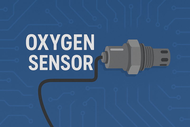 What is an Oxygen Sensor?
24 April 202513140
 Challenges in Enhancing Power Electronic Systems with Artificial Intelligence
26 December 20233124
 Best Practices for Panel Meter Maintenance
11 July 20251355
 Comprehensive Introduction to Snapdragon 888
28 June 202115522
 How to Design a High-precision ADC?
13 December 20212539
 Apple Will Help TSMC to Be in the Leading Position in the Next Era
16 March 20223433
 What is a Vibration Sensor?
24 October 20253195
 A simple guide to flow sensors and their working principle
15 July 20251226
Linear Technology/Analog Devices
In Stock: 960
United States
China
Canada
Japan
Russia
Germany
United Kingdom
Singapore
Italy
Hong Kong(China)
Taiwan(China)
France
Korea
Mexico
Netherlands
Malaysia
Austria
Spain
Switzerland
Poland
Thailand
Vietnam
India
United Arab Emirates
Afghanistan
Åland Islands
Albania
Algeria
American Samoa
Andorra
Angola
Anguilla
Antigua & Barbuda
Argentina
Armenia
Aruba
Australia
Azerbaijan
Bahamas
Bahrain
Bangladesh
Barbados
Belarus
Belgium
Belize
Benin
Bermuda
Bhutan
Bolivia
Bonaire, Sint Eustatius and Saba
Bosnia & Herzegovina
Botswana
Brazil
British Indian Ocean Territory
British Virgin Islands
Brunei
Bulgaria
Burkina Faso
Burundi
Cabo Verde
Cambodia
Cameroon
Cayman Islands
Central African Republic
Chad
Chile
Christmas Island
Cocos (Keeling) Islands
Colombia
Comoros
Congo
Congo (DRC)
Cook Islands
Costa Rica
Côte d’Ivoire
Croatia
Cuba
Curaçao
Cyprus
Czechia
Denmark
Djibouti
Dominica
Dominican Republic
Ecuador
Egypt
El Salvador
Equatorial Guinea
Eritrea
Estonia
Eswatini
Ethiopia
Falkland Islands
Faroe Islands
Fiji
Finland
French Guiana
French Polynesia
Gabon
Gambia
Georgia
Ghana
Gibraltar
Greece
Greenland
Grenada
Guadeloupe
Guam
Guatemala
Guernsey
Guinea
Guinea-Bissau
Guyana
Haiti
Honduras
Hungary
Iceland
Indonesia
Iran
Iraq
Ireland
Isle of Man
Israel
Jamaica
Jersey
Jordan
Kazakhstan
Kenya
Kiribati
Kosovo
Kuwait
Kyrgyzstan
Laos
Latvia
Lebanon
Lesotho
Liberia
Libya
Liechtenstein
Lithuania
Luxembourg
Macao(China)
Madagascar
Malawi
Maldives
Mali
Malta
Marshall Islands
Martinique
Mauritania
Mauritius
Mayotte
Micronesia
Moldova
Monaco
Mongolia
Montenegro
Montserrat
Morocco
Mozambique
Myanmar
Namibia
Nauru
Nepal
New Caledonia
New Zealand
Nicaragua
Niger
Nigeria
Niue
Norfolk Island
North Korea
North Macedonia
Northern Mariana Islands
Norway
Oman
Pakistan
Palau
Palestinian Authority
Panama
Papua New Guinea
Paraguay
Peru
Philippines
Pitcairn Islands
Portugal
Puerto Rico
Qatar
Réunion
Romania
Rwanda
Samoa
San Marino
São Tomé & Príncipe
Saudi Arabia
Senegal
Serbia
Seychelles
Sierra Leone
Sint Maarten
Slovakia
Slovenia
Solomon Islands
Somalia
South Africa
South Sudan
Sri Lanka
St Helena, Ascension, Tristan da Cunha
St. Barthélemy
St. Kitts & Nevis
St. Lucia
St. Martin
St. Pierre & Miquelon
St. Vincent & Grenadines
Sudan
Suriname
Svalbard & Jan Mayen
Sweden
Syria
Tajikistan
Tanzania
Timor-Leste
Togo
Tokelau
Tonga
Trinidad & Tobago
Tunisia
Turkey
Turkmenistan
Turks & Caicos Islands
Tuvalu
U.S. Outlying Islands
U.S. Virgin Islands
Uganda
Ukraine
Uruguay
Uzbekistan
Vanuatu
Vatican City
Venezuela
Wallis & Futuna
Yemen
Zambia
Zimbabwe
![AD826AR-REEL7]() AD826AR-REEL7
AD826AR-REEL7Analog Devices Inc.
![AD8062ARM]() AD8062ARM
AD8062ARMAnalog Devices Inc.
![AD8532ARU-REEL]() AD8532ARU-REEL
AD8532ARU-REELAnalog Devices Inc.
![OP113ES]() OP113ES
OP113ESAnalog Devices Inc.
![SSM2142P]() SSM2142P
SSM2142PAnalog Devices, Inc.
![LTC1050CS8]() LTC1050CS8
LTC1050CS8Linear Technology/Analog Devices
![AMP02EPZ]() AMP02EPZ
AMP02EPZAnalog Devices Inc.
![AD822ARZ-REEL7]() AD822ARZ-REEL7
AD822ARZ-REEL7Analog Devices Inc.
![OP2177ARZ-REEL7]() OP2177ARZ-REEL7
OP2177ARZ-REEL7Analog Devices Inc.
![AD8066ARZ-R7]() AD8066ARZ-R7
AD8066ARZ-R7Analog Devices Inc.


