
 Product
 Brand
Brand Articles
 Tools
Tools
onsemi BCP54 Guide for Amplifier and Switching Circuits


Trans GP BJT PNP 80V 1A 1600mW Automotive 4-Pin(3 Tab) SOT-223 T/R
onsemi BCP54 enables efficient amplifier and switching circuits with reliable current, voltage, and gain—ideal for audio, relay, and power control designs.
Product Introduction
You can use the onsemi bcp54 transistor in many practical ways. This transistor works well when you need to build a circuit for low-power switching or signal amplification. You might see it in driver circuits, power management, or even audio amplification. Many people choose the onsemi bcp54 because it fits surface-mount designs and helps control voltage or regulate current. Focus on using the right setup so your circuit stays reliable and efficient in every application.
Common uses include:
Driving motors
LED control
Battery saver circuits
Switching devices
Power system circuits
onsemi BCP54 Transistor Overview
Key Features
You can count on the onsemi bcp54 transistor for many important tasks in your circuit designs. This bipolar device handles both switching and amplifier roles with ease. You get a strong combination of current, voltage, and gain ratings that make it reliable for many projects.
Here is a quick look at the main electrical characteristics:
| Parameter | Value |
|---|---|
| Maximum Collector Current (Ic) | 1 A |
| Collector-Emitter Voltage (Vceo Max) | 45 V |
| Power Dissipation (Pd) | 1.5 W |
The onsemi bcp54 transistor gives you a high collector current, so you can drive loads up to 1 amp. The maximum collector-emitter voltage of 45 volts means you can use it in circuits with higher voltage needs. You also get a power dissipation rating of 1.5 watts, which helps your circuit stay cool and safe.
You will find three different current gain options, with hFE values ranging from 63 to 250. This wide gain range lets you pick the right transistor for your amplifier or switching circuit. The transition frequency of at least 100 MHz means you can use this transistor for fast switching jobs.
Tip: The onsemi bcp54 comes in a compact SOT-223 package. This makes it easy to fit on crowded circuit boards.
Suitability
You should choose the onsemi bcp54 when you need a bipolar transistor that works well in both amplifier and switching circuits. The high gain and voltage ratings help you build stable amplifier stages. You can use it to boost weak signals or drive speakers in audio circuits.
For switching, the onsemi bcp54 handles fast changes in voltage and current. You can use it to control relays, LEDs, or even small motors. The transistor’s automotive qualification (AEC-Q101) means it stays reliable in tough environments.
Here is a summary of what makes the onsemi bcp54 effective for switching:
| Feature/Specification | Description/Value |
|---|---|
| High collector current capability | Supports collector currents up to 1000mA |
| Current gain selections | Offers three different current gain options (hFE min 63 to max 250) |
| Power dissipation capability | Can dissipate up to 650 mW of power |
| Maximum collector-emitter voltage | Rated for up to 45 V |
| Transition frequency (fT) | Minimum 100 MHz enabling fast switching |
| Automotive qualification | Certified to AEC-Q101 standard ensuring robustness and reliability |
| Recommended applications | Efficient power regulation, fast MOSFET control, reliable switching |
You can trust this transistor for both amplifier and switching circuit designs. Its voltage, gain, and current ratings give you the flexibility to solve many design problems.
Amplifier Circuits
Common-Emitter Amplifier
You can build a common-emitter amplifier using the onsemi BCP54 transistor. This circuit lets you boost weak signals and create a high-gain amplifier for many applications. The common-emitter amplifier uses the transistor with the emitter connected to ground. The input signal goes to the base, and the output comes from the collector. You get a large voltage gain because the common-emitter design multiplies the input signal.
Here is a simple example of a common-emitter amplifier:
Input Signal
   │
   ├───[Coupling Capacitor]───┬───[Base Resistor]───┬───[Base] (BCP54)
                              │                    │
                             [Biasing Resistor]   [Emitter]───[Emitter Resistor]───GND
                              │                    │
                             GND                 [Collector]───[Load Resistor]───Vcc
                                                   │
                                               Output Signal
You can see that the common-emitter amplifier uses resistors for biasing and load selection. The circuit gives you a strong voltage gain and works well for audio or sensor signals.
Biasing
You must set up proper biasing for your common-emitter amplifier. Biasing means you set the base voltage and current so the transistor works in its active region. Good biasing keeps the amplifier stable and prevents distortion. You can use a voltage divider with two resistors to set the base voltage. This method gives you a steady biasing point.
Tip: Always check the biasing resistors. If you choose the wrong values, the common-emitter amplifier may not work as expected.
You should also add an emitter resistor. This resistor improves biasing stability and helps control the voltage gain. The emitter resistor keeps the transistor from overheating and makes the amplifier more reliable.
Load Selection
You need to pick the right load resistor for your common-emitter amplifier. The load resistor connects to the collector and sets the output voltage swing. A larger load resistor gives you higher voltage gain, but it can reduce the output current. A smaller load resistor lowers the voltage gain but allows more current to flow.
You can use this table to help select the right load resistor for your circuit:
| Load Resistor Value | Voltage Gain | Output Current |
|---|---|---|
| High | High | Low |
| Medium | Medium | Medium |
| Low | Low | High |
You should balance voltage gain and output current for your application. If you want a high-gain amplifier, use a higher load resistor. If you need more output current, choose a lower value.
Tips
Always use a bypass capacitor across the emitter resistor. This increases the voltage gain of your common-emitter amplifier.
Check the biasing network often. Small changes in resistor values can affect the voltage gain and stability.
Use the onsemi BCP54 transistor for both common-emitter and common-base amplifier circuits. The transistor works well in both roles.
If you need a high-gain amplifier, use the common-emitter design. For better frequency response, try a common-base amplifier.
Keep the input and output wires short. This reduces noise and keeps your amplifier circuit stable.
Test your amplifier with different load resistors. You will see how the voltage gain changes.
Make sure the power supply voltage matches the needs of your amplifier circuit.
Use heat sinks if your circuit gets warm. This protects the transistor and keeps the voltage gain stable.
Try building both common-emitter and common-base amplifier circuits. You will learn how each design affects voltage gain and signal quality.
Always check the datasheet for the onsemi BCP54 transistor. You will find important information for biasing and voltage gain.
Note: The common-emitter amplifier gives you high gain and strong voltage amplification. The common-base amplifier works better for high-frequency signals but gives lower voltage gain.
Switching Circuits
The onsemi BCP54 transistor works well as a switch in many types of circuit. You can use it to control loads up to 1.5A. This makes it a good choice for relay drivers, digital switches, and other switching applications. You get reliable performance and fast response when you use the BCP54 in your circuit.
Relay Driver
You can use the BCP54 transistor to drive a relay in your circuit. A relay lets you control a high-power device with a low-power signal. Connect the relay coil between the collector and the supply voltage. Place the emitter to ground. When you apply a base current, the transistor switches on. The relay coil gets current and activates the relay contacts.
A simple relay driver circuit looks like this:
Vcc
 │
[Relay Coil]
 │
Collector (BCP54)
Base ──[Base Resistor]── Signal Input
Emitter ── GND
You should always add a flyback diode across the relay coil. This protects the transistor from voltage spikes when the relay turns off. The BCP54 can handle the current needed for most small relays. Make sure the relay coil current does not exceed 1.5A. This keeps your circuit safe and reliable.
Digital Switch
You can use the BCP54 as a digital switch in your circuit. This means you turn a load on or off with a digital signal. The transistor acts like an electronic switch. When you apply a high signal to the base, the transistor turns on. Current flows from collector to emitter, and the load gets power.
The BCP54 gives you fast switching and low saturation voltage. This helps your circuit work efficiently. Here is a table with important switching characteristics:
| Parameter | Value |
|---|---|
| Saturation Voltage (Vce(sat)) | Max 500mV @ Ib=50mA, Ic=500mA |
| Collector Current (Ic) (Max) | 1.5 A |
| Collector-Emitter Breakdown Voltage | 45 V |
| DC Current Gain (hFE) (Min) | 40 @ Ic=150mA, Vce=2V |
| Power Dissipation (Max) | 1.5 W |
A low saturation voltage means less power loss in your circuit. The BCP54 can switch loads quickly, so you can use it in digital control circuits, LED drivers, and logic-level switching.
Protection
You must protect your circuit and the BCP54 transistor from damage. Use a flyback diode when switching inductive loads like relays or motors. This diode blocks high voltage spikes that can destroy the transistor. Place the diode across the load, with the cathode to the supply voltage.
You should also use a base resistor to limit the base current. This keeps the transistor safe and prevents overheating. Choose a resistor value that gives enough base current for full saturation, but not too much.
Tip: Always check the maximum voltage and current ratings for your circuit. Do not exceed the BCP54’s limits.
Thermal Management
The BCP54 can handle up to 1.5W of power dissipation. If your circuit switches high currents or runs for a long time, the transistor can get hot. Heat can damage the transistor and reduce its life.
You should keep the transistor cool. Use a heat sink if your circuit gets warm. Make sure there is good airflow around the transistor. You can also use a larger copper area on the PCB to help spread the heat.
Note: If you keep the temperature low, your circuit will last longer and work better.
Tips
Use the BCP54 for switching loads up to 1.5A in your circuit.
Always add a flyback diode for inductive loads to protect against voltage spikes.
Check the voltage and current ratings before you build your circuit.
Use a base resistor to control the base current and keep the transistor safe.
Keep the transistor cool with a heat sink or good PCB layout.
Test your circuit with the actual load to make sure the transistor does not overheat.
Use the BCP54 for both relay drivers and digital switches. It works well in both types of circuit.
Keep your wiring short and neat. This helps prevent noise and voltage drops in your circuit.
Read the datasheet for more details about voltage, current, and power ratings.
Try different loads in your circuit to see how the BCP54 performs.
Advanced Configurations
Darlington Pair
You can use the onsemi BCP54 transistor in a Darlington pair to get very-high-gain in your circuit. A Darlington pair connects two transistors so the current from the first one feeds into the second. This setup gives you a much higher gain than a single transistor. You often use this when you need a high-gain amplifier or want to switch a load with a very small input signal.
A Darlington pair can boost the voltage gain in your amplifier circuit. You connect the emitter of the first transistor to the base of the second. The collector of both transistors joins together. This design gives you a very-high-gain and strong voltage gain. You can use this for sensor circuits or audio amplifiers that need to pick up weak signals.
Tip: Always check the total voltage drop across a Darlington pair. The voltage drop is higher than with a single transistor.
Complementary Circuits
You can build complementary circuits using the BCP54 with a matching PNP transistor. This setup works well for push-pull amplifier designs. In a push-pull amplifier, one transistor handles the positive half of the signal, and the other handles the negative half. This design gives you better voltage gain and reduces distortion.
A complementary circuit can improve the efficiency of your amplifier. You get a balanced output and higher gain. You often see this in audio amplifier circuits where clean sound is important. The common-base amplifier design also benefits from complementary circuits, giving you stable voltage gain and better performance at higher frequencies.
Use complementary circuits for:
Audio amplifier output stages
Power amplifier designs
Circuits needing balanced voltage gain
High-Speed Switching
You can use the BCP54 for high-speed switching in your circuit. This transistor switches on and off quickly, making it great for digital circuits and pulse amplifiers. Fast switching helps you keep the voltage gain high and the signal clean.
A common-base amplifier circuit often uses the BCP54 for high-speed jobs. The common-base design gives you low input impedance and high voltage gain. You can use this for radio-frequency amplifiers or circuits that need to handle fast signals.
| Configuration | Best Use Case | Voltage Gain | Gain Level |
|---|---|---|---|
| Darlington Pair | Very-High-Gain Amplifier | Very High | Very-High-Gain |
| Complementary Circuit | Push-Pull Amplifier | High | High-Gain |
| Common-Base Amplifier | High-Speed Switching | High | High-Gain |
Remember: The common-base amplifier gives you high voltage gain and works well for high-frequency signals.
Troubleshooting
Common Issues
You may face some problems when you build a common-emitter amplifier. Sometimes, you see low gain or no output. This can happen if you use the wrong resistor values in your common-emitter circuit. If you forget to set proper biasing, the transistor may not work in the active region. You might also notice noise or distortion in your amplifier. Loose connections or long wires can cause these problems.
Here are some common issues you might see:
The common-emitter amplifier does not amplify the signal.
The output signal looks distorted.
The gain is much lower than expected.
The circuit gets too hot.
Tip: Always double-check your resistor values and connections in the common-emitter stage.
Reliability
You want your amplifier to work well every time. To keep your common-emitter circuit reliable, use good quality parts. Make sure the transistor does not get too hot. If you use the BCP54 in a common-emitter amplifier, add a heat sink if needed. Keep the gain at a safe level. Too much gain can make the circuit unstable. Use a bypass capacitor to help the common-emitter amplifier stay stable. Good biasing also helps your amplifier last longer.
A reliable amplifier gives you clear sound and strong performance. You can trust your common-emitter design if you follow these tips.
Checklist
Use this checklist to solve problems in your common-emitter amplifier:
| Step | What to Check |
|---|---|
| 1 | Are all common-emitter connections tight? |
| 2 | Did you use the right resistor values? |
| 3 | Is the biasing set for the active region? |
| 4 | Does the gain match your needs? |
| 5 | Is the transistor cool during use? |
| 6 | Did you add a bypass capacitor? |
| 7 | Are wires short and neat? |
If you follow this checklist, you can fix most problems in your common-emitter amplifier. You will get better gain and more stable output.
You can use the onsemi BCP54 transistor to build both amplifier and switching circuits with confidence. Focus on proper biasing, load selection, and thermal management for reliable results. Always check the datasheet and explore onsemi’s tools like the Product Recommendation Tools+ and Elite Power Simulator for better designs. Try different setups and learn from real-world testing. For more help, use these resources:
| Resource Type | What You Get |
|---|---|
| Datasheet | Full specs and ratings |
| Application Notes | Practical circuit tips |
| Simulation Models | Test your ideas before building |
| System Solution Guides | Application-specific advice |
Keep experimenting and apply your knowledge to real projects for the best learning experience!
FAQ
What is the maximum current you can safely switch with the onsemi BCP54?
You can safely switch up to 1.5A with the onsemi BCP54. Always check your load and make sure the transistor stays cool. Use a heat sink if needed to prevent overheating.
Can you use the BCP54 for audio amplifier circuits?
Yes, you can use the BCP54 in audio amplifier circuits. It works well in common-emitter and push-pull designs. You get good voltage gain and reliable performance for small speaker or signal applications.
Do you need a flyback diode when switching relays or motors?
Yes, always use a flyback diode across the relay coil or motor. This protects the BCP54 from voltage spikes that can damage the transistor when you turn off the load.
How do you choose the right base resistor for switching?
You should calculate the base resistor so the base current is about one-tenth of the collector current. For example, if your load needs 1A, set the base current to 100mA. Use Ohm’s Law to find the resistor value.
What package does the onsemi BCP54 come in?
The onsemi BCP54 comes in a SOT-223 surface-mount package. This package saves space on your circuit board and helps with heat dissipation.
Specifications
- TypeParameter
- Lifecycle Status
Lifecycle Status refers to the current stage of an electronic component in its product life cycle, indicating whether it is active, obsolete, or transitioning between these states. An active status means the component is in production and available for purchase. An obsolete status indicates that the component is no longer being manufactured or supported, and manufacturers typically provide a limited time frame for support. Understanding the lifecycle status is crucial for design engineers to ensure continuity and reliability in their projects.
ACTIVE (Last Updated: 8 months ago) - Factory Lead Time8 Weeks
- Contact Plating
Contact plating (finish) provides corrosion protection for base metals and optimizes the mechanical and electrical properties of the contact interfaces.
Tin - Mount
In electronic components, the term "Mount" typically refers to the method or process of physically attaching or fixing a component onto a circuit board or other electronic device. This can involve soldering, adhesive bonding, or other techniques to secure the component in place. The mounting process is crucial for ensuring proper electrical connections and mechanical stability within the electronic system. Different components may have specific mounting requirements based on their size, shape, and function, and manufacturers provide guidelines for proper mounting procedures to ensure optimal performance and reliability of the electronic device.
Surface Mount - Mounting Type
The "Mounting Type" in electronic components refers to the method used to attach or connect a component to a circuit board or other substrate, such as through-hole, surface-mount, or panel mount.
Surface Mount - Package / Case
refers to the protective housing that encases an electronic component, providing mechanical support, electrical connections, and thermal management.
TO-261-4, TO-261AA - Number of Pins4
- Transistor Element Material
The "Transistor Element Material" parameter in electronic components refers to the material used to construct the transistor within the component. Transistors are semiconductor devices that amplify or switch electronic signals and are a fundamental building block in electronic circuits. The material used for the transistor element can significantly impact the performance and characteristics of the component. Common materials used for transistor elements include silicon, germanium, and gallium arsenide, each with its own unique properties and suitability for different applications. The choice of transistor element material is crucial in designing electronic components to meet specific performance requirements such as speed, power efficiency, and temperature tolerance.
SILICON - Collector-Emitter Breakdown Voltage80V
- Collector-Emitter Saturation Voltage-500mV
- Number of Elements1
- hFEMin40
- Operating Temperature
The operating temperature is the range of ambient temperature within which a power supply, or any other electrical equipment, operate in. This ranges from a minimum operating temperature, to a peak or maximum operating temperature, outside which, the power supply may fail.
150°C TJ - Packaging
Semiconductor package is a carrier / shell used to contain and cover one or more semiconductor components or integrated circuits. The material of the shell can be metal, plastic, glass or ceramic.
Cut Tape (CT) - JESD-609 Code
The "JESD-609 Code" in electronic components refers to a standardized marking code that indicates the lead-free solder composition and finish of electronic components for compliance with environmental regulations.
e3 - Part Status
Parts can have many statuses as they progress through the configuration, analysis, review, and approval stages.
Active - Moisture Sensitivity Level (MSL)
Moisture Sensitivity Level (MSL) is a standardized rating that indicates the susceptibility of electronic components, particularly semiconductors, to moisture-induced damage during storage and the soldering process, defining the allowable exposure time to ambient conditions before they require special handling or baking to prevent failures
1 (Unlimited) - Number of Terminations4
- ECCN Code
An ECCN (Export Control Classification Number) is an alphanumeric code used by the U.S. Bureau of Industry and Security to identify and categorize electronic components and other dual-use items that may require an export license based on their technical characteristics and potential for military use.
EAR99 - Max Power Dissipation
The maximum power that the MOSFET can dissipate continuously under the specified thermal conditions.
1.6W - Terminal Position
In electronic components, the term "Terminal Position" refers to the physical location of the connection points on the component where external electrical connections can be made. These connection points, known as terminals, are typically used to attach wires, leads, or other components to the main body of the electronic component. The terminal position is important for ensuring proper connectivity and functionality of the component within a circuit. It is often specified in technical datasheets or component specifications to help designers and engineers understand how to properly integrate the component into their circuit designs.
DUAL - Terminal Form
Occurring at or forming the end of a series, succession, or the like; closing; concluding.
GULL WING - Peak Reflow Temperature (Cel)
Peak Reflow Temperature (Cel) is a parameter that specifies the maximum temperature at which an electronic component can be exposed during the reflow soldering process. Reflow soldering is a common method used to attach electronic components to a circuit board. The Peak Reflow Temperature is crucial because it ensures that the component is not damaged or degraded during the soldering process. Exceeding the specified Peak Reflow Temperature can lead to issues such as component failure, reduced performance, or even permanent damage to the component. It is important for manufacturers and assemblers to adhere to the recommended Peak Reflow Temperature to ensure the reliability and functionality of the electronic components.
260 - Frequency
In electronic components, the parameter "Frequency" refers to the rate at which a signal oscillates or cycles within a given period of time. It is typically measured in Hertz (Hz) and represents how many times a signal completes a full cycle in one second. Frequency is a crucial aspect in electronic components as it determines the behavior and performance of various devices such as oscillators, filters, and communication systems. Understanding the frequency characteristics of components is essential for designing and analyzing electronic circuits to ensure proper functionality and compatibility with other components in a system.
50MHz - Time@Peak Reflow Temperature-Max (s)
Time@Peak Reflow Temperature-Max (s) refers to the maximum duration that an electronic component can be exposed to the peak reflow temperature during the soldering process, which is crucial for ensuring reliable solder joint formation without damaging the component.
30 - Base Part Number
The "Base Part Number" (BPN) in electronic components serves a similar purpose to the "Base Product Number." It refers to the primary identifier for a component that captures the essential characteristics shared by a group of similar components. The BPN provides a fundamental way to reference a family or series of components without specifying all the variations and specific details.
BCP53 - Pin Count
a count of all of the component leads (or pins)
4 - Element Configuration
The distribution of electrons of an atom or molecule (or other physical structure) in atomic or molecular orbitals.
Single - Power Dissipation
the process by which an electronic or electrical device produces heat (energy loss or waste) as an undesirable derivative of its primary action.
1.6W - Case Connection
Case Connection refers to the method by which an electronic component's case or housing is connected to the electrical circuit. This connection is important for grounding purposes, mechanical stability, and heat dissipation. The case connection can vary depending on the type of component and its intended application. It is crucial to ensure a secure and reliable case connection to maintain the overall performance and safety of the electronic device.
COLLECTOR - Transistor Application
In the context of electronic components, the parameter "Transistor Application" refers to the specific purpose or function for which a transistor is designed and used. Transistors are semiconductor devices that can amplify or switch electronic signals and are commonly used in various electronic circuits. The application of a transistor can vary widely depending on its design and characteristics, such as whether it is intended for audio amplification, digital logic, power control, or radio frequency applications. Understanding the transistor application is important for selecting the right type of transistor for a particular circuit or system to ensure optimal performance and functionality.
SWITCHING - Gain Bandwidth Product
The gain–bandwidth product (designated as GBWP, GBW, GBP, or GB) for an amplifier is the product of the amplifier's bandwidth and the gain at which the bandwidth is measured.
50MHz - Polarity/Channel Type
In electronic components, the parameter "Polarity/Channel Type" refers to the characteristic that determines the direction of current flow or the type of signal that can be accommodated by the component. For components like diodes and transistors, polarity indicates the direction in which current can flow through the component, such as forward bias or reverse bias for diodes. For components like MOSFETs or JFETs, the channel type refers to whether the component is an N-channel or P-channel device, which determines the type of charge carriers that carry current through the component. Understanding the polarity or channel type of a component is crucial for proper circuit design and ensuring that the component is connected correctly to achieve the desired functionality.
PNP - Transistor Type
Transistor type refers to the classification of transistors based on their operation and construction. The two primary types are bipolar junction transistors (BJTs) and field-effect transistors (FETs). BJTs use current to control the flow of current, while FETs utilize voltage to control current flow. Each type has its own subtypes, such as NPN and PNP for BJTs, and MOSFETs and JFETs for FETs, impacting their applications and characteristics in electronic circuits.
PNP - Collector Emitter Voltage (VCEO)
Collector-Emitter Voltage (VCEO) is a key parameter in electronic components, particularly in transistors. It refers to the maximum voltage that can be applied between the collector and emitter terminals of a transistor while the base terminal is open or not conducting. Exceeding this voltage limit can lead to breakdown and potential damage to the transistor. VCEO is crucial for ensuring the safe and reliable operation of the transistor within its specified limits. Designers must carefully consider VCEO when selecting transistors for a circuit to prevent overvoltage conditions that could compromise the performance and longevity of the component.
80V - Max Collector Current
Max Collector Current is a parameter used to specify the maximum amount of current that can safely flow through the collector terminal of a transistor or other electronic component without causing damage. It is typically expressed in units of amperes (A) and is an important consideration when designing circuits to ensure that the component operates within its safe operating limits. Exceeding the specified max collector current can lead to overheating, degradation of performance, or even permanent damage to the component. Designers must carefully consider this parameter when selecting components and designing circuits to ensure reliable and safe operation.
1A - DC Current Gain (hFE) (Min) @ Ic, Vce
The parameter "DC Current Gain (hFE) (Min) @ Ic, Vce" in electronic components refers to the minimum value of the DC current gain, denoted as hFE, under specific operating conditions of collector current (Ic) and collector-emitter voltage (Vce). The DC current gain hFE represents the ratio of the collector current to the base current in a bipolar junction transistor (BJT), indicating the amplification capability of the transistor. The minimum hFE value at a given Ic and Vce helps determine the transistor's performance and efficiency in amplifying signals within a circuit. Designers use this parameter to ensure proper transistor selection and performance in various electronic applications.
100 @ 150mA 2V - Current - Collector Cutoff (Max)
The parameter "Current - Collector Cutoff (Max)" refers to the maximum current at which a transistor or other electronic component will cease to conduct current between the collector and emitter terminals. This parameter is important in determining the maximum current that can flow through the component when it is in the cutoff state. Exceeding this maximum cutoff current can lead to malfunction or damage of the component. It is typically specified in the component's datasheet and is crucial for proper circuit design and operation.
100nA ICBO - Vce Saturation (Max) @ Ib, Ic
The parameter "Vce Saturation (Max) @ Ib, Ic" in electronic components refers to the maximum voltage drop across the collector-emitter junction when the transistor is in saturation mode. This parameter is specified at a certain base current (Ib) and collector current (Ic) levels. It indicates the minimum voltage required to keep the transistor fully conducting in saturation mode, ensuring that the transistor operates efficiently and does not enter the cutoff region. Designers use this parameter to ensure proper transistor operation and to prevent overheating or damage to the component.
500mV @ 50mA, 500mA - Transition Frequency
Transition Frequency in electronic components refers to the frequency at which a device can transition from one state to another, typically defining the upper limit of its operating frequency. It is a critical parameter in determining the speed and performance of active components like transistors and integrated circuits. This frequency is influenced by factors such as capacitance, resistance, and the inherent characteristics of the materials used in the component's construction. Understanding transition frequency is essential for optimizing circuit designs and ensuring reliable signal processing in various applications.
50MHz - Max Breakdown Voltage
The "Max Breakdown Voltage" of an electronic component refers to the maximum voltage that the component can withstand across its terminals before it breaks down and allows current to flow uncontrollably. This parameter is crucial in determining the operating limits and safety margins of the component in a circuit. Exceeding the maximum breakdown voltage can lead to permanent damage or failure of the component. It is typically specified by the manufacturer in datasheets to guide engineers and designers in selecting the appropriate components for their applications.
80V - Collector Base Voltage (VCBO)
Collector Base Voltage (VCBO) is the maximum allowable voltage that can be applied between the collector and base terminals of a bipolar junction transistor when the emitter is open. It is a critical parameter that determines the voltage rating of the transistor and helps prevent breakdown in the collector-base junction. Exceeding this voltage can lead to permanent damage or failure of the component.
100V - Emitter Base Voltage (VEBO)
Emitter Base Voltage (VEBO) is a parameter used in electronic components, particularly in transistors. It refers to the maximum voltage that can be applied between the emitter and base terminals of a transistor without causing damage to the device. Exceeding this voltage limit can lead to breakdown of the transistor and potential failure. VEBO is an important specification to consider when designing circuits to ensure the proper operation and reliability of the components. It is typically provided in the datasheet of the transistor and should be carefully observed to prevent any potential damage during operation.
5V - Radiation Hardening
Radiation hardening is the process of making electronic components and circuits resistant to damage or malfunction caused by high levels of ionizing radiation, especially for environments in outer space (especially beyond the low Earth orbit), around nuclear reactors and particle accelerators, or during nuclear accidents or nuclear warfare.
No - RoHS Status
RoHS means “Restriction of Certain Hazardous Substances” in the “Hazardous Substances Directive” in electrical and electronic equipment.
ROHS3 Compliant
Parts with Similar Specs
- ImagePart NumberManufacturerMountPackage / CaseCollector Emitter Breakdown VoltageMax Collector CurrentTransition FrequencyCollector Emitter Saturation VoltagehFE MinMax Power DissipationView Compare
![BCP53-16]()
BCP53-16
Surface Mount
TO-261-4, TO-261AA
80 V
1 A
50 MHz
-500 mV
40
1.6 W
![BCP53TA]()
Surface Mount
TO-261-4, TO-261AA
60 V
1.2 A
-
500 mV
40
1.5 W
![BCP52]()
Surface Mount
TO-261-4, TO-261AA
80 V
1 A
150 MHz
-500 mV
-
2 W
![BCP5316TA]()
Surface Mount
TO-261-4, TO-261AA
80 V
1.5 A
-
-500 mV
25
1.5 W
![BCP53]()
Surface Mount
TO-261-4, TO-261AA
80 V
1 A
150 MHz
500 mV
40
2 W


Datasheet PDF
- Datasheets :
![PC817 Optocoupler: PC817 vs EL817 Pinout, Schematic, Equivalent [FAQ]](https://res.utmel.com/Images/Article/6a882619-81b5-4cff-8d9e-f8f601980f58.jpg) PC817 Optocoupler: PC817 vs EL817 Pinout, Schematic, Equivalent [FAQ]
PC817 Optocoupler: PC817 vs EL817 Pinout, Schematic, Equivalent [FAQ]03 September 202224419
 A Comprehensive Guide to the RV-8803 Real-Time Clock Module
11 March 20241773
 AD8397 310mA High-Output Op-Amp: Performance Analysis and PCB Layout Handbook
14 March 2026138
 TPS92630QPWPRQ1 LED Driver: Pinout, Manufacturer, and Datasheet
23 March 2022325
 XC6206 Low ESR Voltage Regulator: Datasheet pdf, Pinout and Equivalents
26 November 20214687
 SN74LV1T34DCKR Shifter: Pinout, Applications and Datasheet
12 December 2023704
.png) STM32G071G8U6 Microcontroller Datasheet Overview
STM32G071G8U6 Microcontroller Datasheet Overview29 February 2024208
![How to Differentiate:74HC595 vs. 74LS595 vs. 74HC164 vs. MCP23017[FAQ&Video]](https://res.utmel.com/Images/Article/3caa28ab-9759-4d2e-8d7c-4475fc79fbbc.jpg) How to Differentiate:74HC595 vs. 74LS595 vs. 74HC164 vs. MCP23017[FAQ&Video]
How to Differentiate:74HC595 vs. 74LS595 vs. 74HC164 vs. MCP23017[FAQ&Video]25 February 20225821
 Introduction to Light-emitting Diode
18 March 20265827
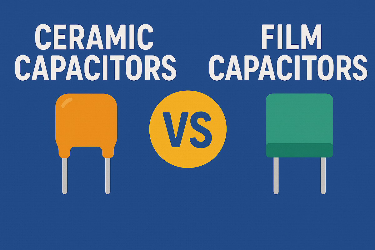 Ceramic Capacitors vs Film Capacitors: A Comprehensive Comparison Guide
14 May 20255251
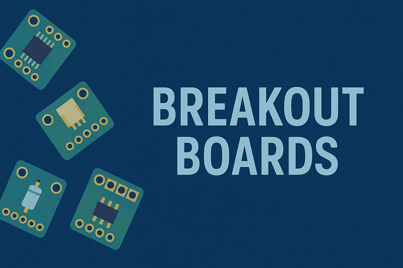 Breakout Boards Alternatives for Your Next Home Project
02 July 20251706
 Basic Knowledge of Various Types of Mixers
03 January 20236305
 Introduction to Graphics Processing Unit (GPU)
26 January 20213427
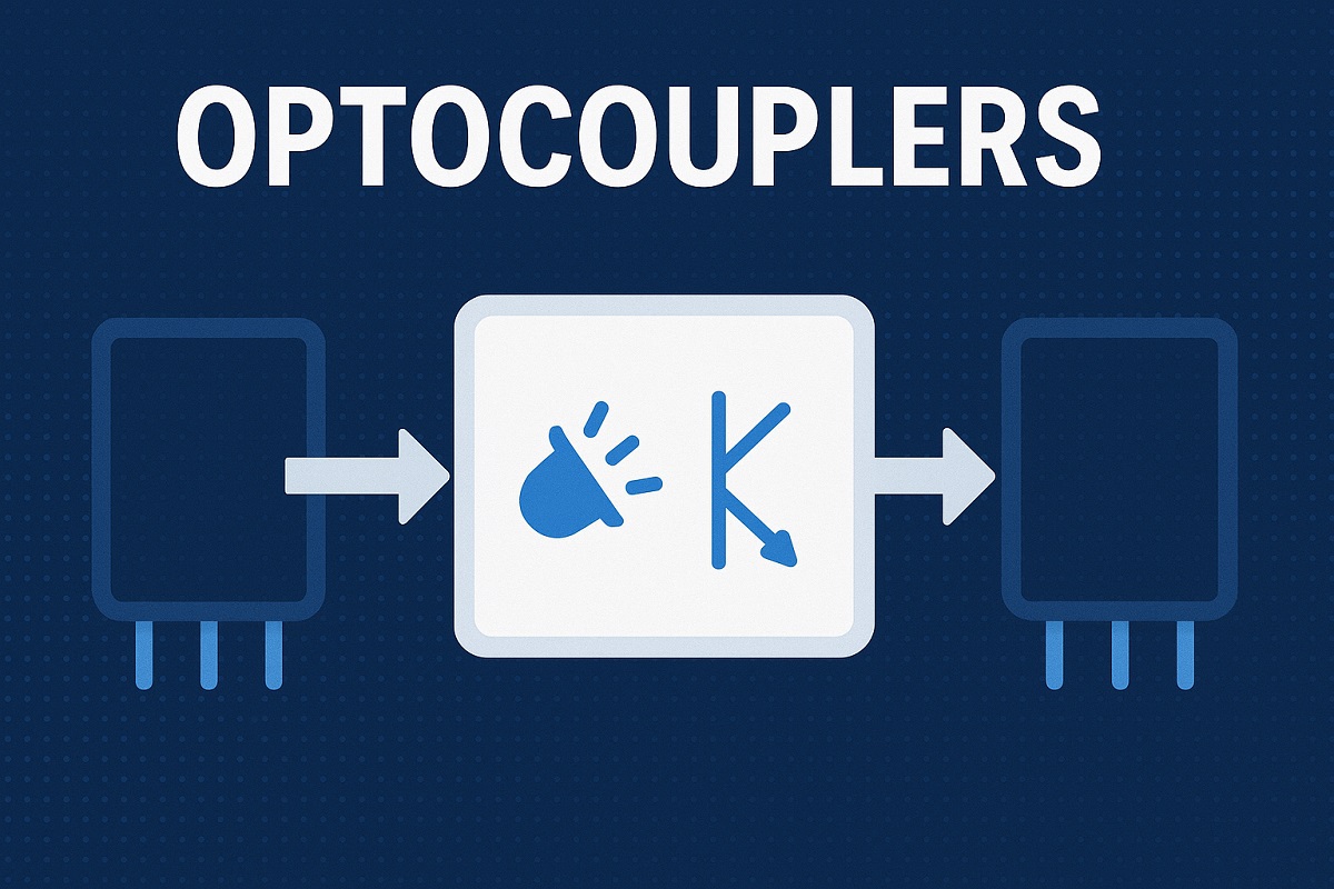 Optocouplers Guide: Understanding Types, Applications, and Circuit Design Tutorial
06 June 20254064
 How does the CPU recognize the Code?
08 August 20221187
 C1815 vs C945 Key Features and Application Guide
01 September 20253602
STMicroelectronics
In Stock: 12000
United States
China
Canada
Japan
Russia
Germany
United Kingdom
Singapore
Italy
Hong Kong(China)
Taiwan(China)
France
Korea
Mexico
Netherlands
Malaysia
Austria
Spain
Switzerland
Poland
Thailand
Vietnam
India
United Arab Emirates
Afghanistan
Åland Islands
Albania
Algeria
American Samoa
Andorra
Angola
Anguilla
Antigua & Barbuda
Argentina
Armenia
Aruba
Australia
Azerbaijan
Bahamas
Bahrain
Bangladesh
Barbados
Belarus
Belgium
Belize
Benin
Bermuda
Bhutan
Bolivia
Bonaire, Sint Eustatius and Saba
Bosnia & Herzegovina
Botswana
Brazil
British Indian Ocean Territory
British Virgin Islands
Brunei
Bulgaria
Burkina Faso
Burundi
Cabo Verde
Cambodia
Cameroon
Cayman Islands
Central African Republic
Chad
Chile
Christmas Island
Cocos (Keeling) Islands
Colombia
Comoros
Congo
Congo (DRC)
Cook Islands
Costa Rica
Côte d’Ivoire
Croatia
Cuba
Curaçao
Cyprus
Czechia
Denmark
Djibouti
Dominica
Dominican Republic
Ecuador
Egypt
El Salvador
Equatorial Guinea
Eritrea
Estonia
Eswatini
Ethiopia
Falkland Islands
Faroe Islands
Fiji
Finland
French Guiana
French Polynesia
Gabon
Gambia
Georgia
Ghana
Gibraltar
Greece
Greenland
Grenada
Guadeloupe
Guam
Guatemala
Guernsey
Guinea
Guinea-Bissau
Guyana
Haiti
Honduras
Hungary
Iceland
Indonesia
Iran
Iraq
Ireland
Isle of Man
Israel
Jamaica
Jersey
Jordan
Kazakhstan
Kenya
Kiribati
Kosovo
Kuwait
Kyrgyzstan
Laos
Latvia
Lebanon
Lesotho
Liberia
Libya
Liechtenstein
Lithuania
Luxembourg
Macao(China)
Madagascar
Malawi
Maldives
Mali
Malta
Marshall Islands
Martinique
Mauritania
Mauritius
Mayotte
Micronesia
Moldova
Monaco
Mongolia
Montenegro
Montserrat
Morocco
Mozambique
Myanmar
Namibia
Nauru
Nepal
New Caledonia
New Zealand
Nicaragua
Niger
Nigeria
Niue
Norfolk Island
North Korea
North Macedonia
Northern Mariana Islands
Norway
Oman
Pakistan
Palau
Palestinian Authority
Panama
Papua New Guinea
Paraguay
Peru
Philippines
Pitcairn Islands
Portugal
Puerto Rico
Qatar
Réunion
Romania
Rwanda
Samoa
San Marino
São Tomé & Príncipe
Saudi Arabia
Senegal
Serbia
Seychelles
Sierra Leone
Sint Maarten
Slovakia
Slovenia
Solomon Islands
Somalia
South Africa
South Sudan
Sri Lanka
St Helena, Ascension, Tristan da Cunha
St. Barthélemy
St. Kitts & Nevis
St. Lucia
St. Martin
St. Pierre & Miquelon
St. Vincent & Grenadines
Sudan
Suriname
Svalbard & Jan Mayen
Sweden
Syria
Tajikistan
Tanzania
Timor-Leste
Togo
Tokelau
Tonga
Trinidad & Tobago
Tunisia
Turkey
Turkmenistan
Turks & Caicos Islands
Tuvalu
U.S. Outlying Islands
U.S. Virgin Islands
Uganda
Ukraine
Uruguay
Uzbekistan
Vanuatu
Vatican City
Venezuela
Wallis & Futuna
Yemen
Zambia
Zimbabwe


