
 Product
 Brand
Brand Articles
 Tools
Tools
2N5457 N-Channel JFET : Pinout, Alternative and Datasheet


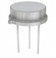
JFET N-CH 25V 625MW TO92
2N5457 is an N Channel JFET (Junction Field Effect Transistor). Today, I am going to uncover the details to 2n5457.You don’t need to go anywhere and you can find all informations here. Let's dive into what it is and how to use it.

JFET Audio Switch Circuit - 2n5457
2N5457 Description
The 2N5457 is an N Channel JFET (Junction Field Effect Transistor) which is mainly designed for audio and switching applications.
It consists of drain, source and gate which are denoted by D, S and G respectively.
It is a voltage control device that does not require any bias current to control the large current on other terminals.
2N5457 Pinout
The 2N5457 has three pins: Drain, source and gate

2N5457 CAD Model
Symbol

Footprint

2N5457 Features
• N channel for higher gain
• Drain and source are interchangeable
• High AC input impedance
• High DC input resistance
• Low transmission and input capacitance
• Low cross-modulation and intermodulation distortion
• Plastic package
• Provide lead-free packaging*
Specifications
- TypeParameter
- Lifecycle Status
Lifecycle Status refers to the current stage of an electronic component in its product life cycle, indicating whether it is active, obsolete, or transitioning between these states. An active status means the component is in production and available for purchase. An obsolete status indicates that the component is no longer being manufactured or supported, and manufacturers typically provide a limited time frame for support. Understanding the lifecycle status is crucial for design engineers to ensure continuity and reliability in their projects.
OBSOLETE (Last Updated: 3 days ago) - Mount
In electronic components, the term "Mount" typically refers to the method or process of physically attaching or fixing a component onto a circuit board or other electronic device. This can involve soldering, adhesive bonding, or other techniques to secure the component in place. The mounting process is crucial for ensuring proper electrical connections and mechanical stability within the electronic system. Different components may have specific mounting requirements based on their size, shape, and function, and manufacturers provide guidelines for proper mounting procedures to ensure optimal performance and reliability of the electronic device.
Through Hole - Package / Case
refers to the protective housing that encases an electronic component, providing mechanical support, electrical connections, and thermal management.
TO-92 - Number of Pins3
- Weight201mg
- Number of Elements1
- Power Dissipation (Max)625mW
- Packaging
Semiconductor package is a carrier / shell used to contain and cover one or more semiconductor components or integrated circuits. The material of the shell can be metal, plastic, glass or ceramic.
Bulk - Published2006
- JESD-609 Code
The "JESD-609 Code" in electronic components refers to a standardized marking code that indicates the lead-free solder composition and finish of electronic components for compliance with environmental regulations.
e0 - Pbfree Code
The "Pbfree Code" parameter in electronic components refers to the code or marking used to indicate that the component is lead-free. Lead (Pb) is a toxic substance that has been widely used in electronic components for many years, but due to environmental concerns, there has been a shift towards lead-free alternatives. The Pbfree Code helps manufacturers and users easily identify components that do not contain lead, ensuring compliance with regulations and promoting environmentally friendly practices. It is important to pay attention to the Pbfree Code when selecting electronic components to ensure they meet the necessary requirements for lead-free applications.
no - Number of Terminations3
- Termination
Termination in electronic components refers to the practice of matching the impedance of a circuit to prevent signal reflections and ensure maximum power transfer. It involves the use of resistors or other components at the end of transmission lines or connections. Proper termination is crucial in high-frequency applications to maintain signal integrity and reduce noise.
Through Hole - ECCN Code
An ECCN (Export Control Classification Number) is an alphanumeric code used by the U.S. Bureau of Industry and Security to identify and categorize electronic components and other dual-use items that may require an export license based on their technical characteristics and potential for military use.
EAR99 - Terminal Finish
Terminal Finish refers to the surface treatment applied to the terminals or leads of electronic components to enhance their performance and longevity. It can improve solderability, corrosion resistance, and overall reliability of the connection in electronic assemblies. Common finishes include nickel, gold, and tin, each possessing distinct properties suitable for various applications. The choice of terminal finish can significantly impact the durability and effectiveness of electronic devices.
Tin/Lead (Sn/Pb) - Max Operating Temperature
The Maximum Operating Temperature is the maximum body temperature at which the thermistor is designed to operate for extended periods of time with acceptable stability of its electrical characteristics.
135°C - Min Operating Temperature
The "Min Operating Temperature" parameter in electronic components refers to the lowest temperature at which the component is designed to operate effectively and reliably. This parameter is crucial for ensuring the proper functioning and longevity of the component, as operating below this temperature may lead to performance issues or even damage. Manufacturers specify the minimum operating temperature to provide guidance to users on the environmental conditions in which the component can safely operate. It is important to adhere to this parameter to prevent malfunctions and ensure the overall reliability of the electronic system.
-55°C - Additional Feature
Any Feature, including a modified Existing Feature, that is not an Existing Feature.
LOW NOISE - HTS Code
HTS (Harmonized Tariff Schedule) codes are product classification codes between 8-1 digits. The first six digits are an HS code, and the countries of import assign the subsequent digits to provide additional classification. U.S. HTS codes are 1 digits and are administered by the U.S. International Trade Commission.
8541.21.00.95 - Voltage - Rated DC
Voltage - Rated DC is a parameter that specifies the maximum direct current (DC) voltage that an electronic component can safely handle without being damaged. This rating is crucial for ensuring the proper functioning and longevity of the component in a circuit. Exceeding the rated DC voltage can lead to overheating, breakdown, or even permanent damage to the component. It is important to carefully consider this parameter when designing or selecting components for a circuit to prevent any potential issues related to voltage overload.
25V - Terminal Position
In electronic components, the term "Terminal Position" refers to the physical location of the connection points on the component where external electrical connections can be made. These connection points, known as terminals, are typically used to attach wires, leads, or other components to the main body of the electronic component. The terminal position is important for ensuring proper connectivity and functionality of the component within a circuit. It is often specified in technical datasheets or component specifications to help designers and engineers understand how to properly integrate the component into their circuit designs.
BOTTOM - Peak Reflow Temperature (Cel)
Peak Reflow Temperature (Cel) is a parameter that specifies the maximum temperature at which an electronic component can be exposed during the reflow soldering process. Reflow soldering is a common method used to attach electronic components to a circuit board. The Peak Reflow Temperature is crucial because it ensures that the component is not damaged or degraded during the soldering process. Exceeding the specified Peak Reflow Temperature can lead to issues such as component failure, reduced performance, or even permanent damage to the component. It is important for manufacturers and assemblers to adhere to the recommended Peak Reflow Temperature to ensure the reliability and functionality of the electronic components.
240 - Current Rating
Current rating is the maximum current that a fuse will carry for an indefinite period without too much deterioration of the fuse element.
10mA - Time@Peak Reflow Temperature-Max (s)
Time@Peak Reflow Temperature-Max (s) refers to the maximum duration that an electronic component can be exposed to the peak reflow temperature during the soldering process, which is crucial for ensuring reliable solder joint formation without damaging the component.
30 - Pin Count
a count of all of the component leads (or pins)
3 - Qualification Status
An indicator of formal certification of qualifications.
Not Qualified - Element Configuration
The distribution of electrons of an atom or molecule (or other physical structure) in atomic or molecular orbitals.
Single - Operating Mode
A phase of operation during the operation and maintenance stages of the life cycle of a facility.
DEPLETION MODE - Power Dissipation
the process by which an electronic or electrical device produces heat (energy loss or waste) as an undesirable derivative of its primary action.
625mW - Transistor Application
In the context of electronic components, the parameter "Transistor Application" refers to the specific purpose or function for which a transistor is designed and used. Transistors are semiconductor devices that can amplify or switch electronic signals and are commonly used in various electronic circuits. The application of a transistor can vary widely depending on its design and characteristics, such as whether it is intended for audio amplification, digital logic, power control, or radio frequency applications. Understanding the transistor application is important for selecting the right type of transistor for a particular circuit or system to ensure optimal performance and functionality.
SWITCHING - Drain to Source Voltage (Vdss)
The Drain to Source Voltage (Vdss) is a key parameter in electronic components, particularly in field-effect transistors (FETs) such as MOSFETs. It refers to the maximum voltage that can be applied between the drain and source terminals of the FET without causing damage to the component. Exceeding this voltage limit can lead to breakdown and potentially permanent damage to the device.Vdss is an important specification to consider when designing or selecting components for a circuit, as it determines the operating range and reliability of the FET. It is crucial to ensure that the Vdss rating of the component is higher than the maximum voltage expected in the circuit to prevent failures and ensure proper functionality.In summary, the Drain to Source Voltage (Vdss) is a critical parameter that defines the maximum voltage tolerance of a FET component and plays a significant role in determining the overall performance and reliability of electronic circuits.
25V - Polarity/Channel Type
In electronic components, the parameter "Polarity/Channel Type" refers to the characteristic that determines the direction of current flow or the type of signal that can be accommodated by the component. For components like diodes and transistors, polarity indicates the direction in which current can flow through the component, such as forward bias or reverse bias for diodes. For components like MOSFETs or JFETs, the channel type refers to whether the component is an N-channel or P-channel device, which determines the type of charge carriers that carry current through the component. Understanding the polarity or channel type of a component is crucial for proper circuit design and ensuring that the component is connected correctly to achieve the desired functionality.
N-CHANNEL - Continuous Drain Current (ID)
Continuous Drain Current (ID) is a key parameter in electronic components, particularly in field-effect transistors (FETs) such as MOSFETs. It refers to the maximum current that can flow continuously through the drain terminal of the FET without causing damage to the component. This parameter is crucial for determining the power handling capability of the FET and is specified by the manufacturer in the component's datasheet. Designers must ensure that the actual operating current does not exceed the specified Continuous Drain Current to prevent overheating and potential failure of the component.
5mA - Gate to Source Voltage (Vgs)
The Gate to Source Voltage (Vgs) is a crucial parameter in electronic components, particularly in field-effect transistors (FETs) such as MOSFETs. It refers to the voltage difference between the gate and source terminals of the FET. This voltage determines the conductivity of the FET and controls the flow of current through the device. By varying the Vgs, the FET can be switched on or off, allowing for precise control of electronic circuits. Understanding and properly managing the Vgs is essential for ensuring the reliable and efficient operation of FET-based circuits.
-25V - FET Technology
Field-Effect Transistor (FET) technology is a type of semiconductor device commonly used in electronic components such as transistors and integrated circuits. FETs operate by controlling the flow of current through a semiconductor channel using an electric field. There are several types of FETs, including Metal-Oxide-Semiconductor FETs (MOSFETs) and Junction FETs (JFETs), each with its own characteristics and applications. FET technology offers advantages such as high input impedance, low power consumption, and fast switching speeds, making it suitable for a wide range of electronic devices and circuits. Overall, FET technology plays a crucial role in modern electronics by enabling efficient and reliable signal processing and amplification.
JUNCTION - Voltage - Breakdown
Voltage - Breakdown is a parameter that refers to the maximum voltage that an electronic component can withstand before it breaks down and allows current to flow through it uncontrollably. This breakdown voltage is a critical specification for components like diodes, transistors, and capacitors, as exceeding this voltage can lead to permanent damage or failure of the component. Manufacturers typically provide this information in datasheets to help engineers and designers ensure the proper operation and reliability of their circuits. It is important to consider the breakdown voltage when designing circuits to prevent overvoltage conditions that could compromise the performance and longevity of the components.
-25V - Capacitance - Input
Capacitance - Input is a parameter that describes the input capacitance of an electronic component, such as a transistor or an integrated circuit. It represents the amount of charge that the input of the component can store when a voltage is applied to it. This capacitance affects the speed and performance of the component, as it can influence the time it takes for the input signal to be processed. A higher input capacitance can result in slower response times and may require additional circuitry to mitigate its effects. It is an important parameter to consider when designing and analyzing electronic circuits to ensure proper functionality and performance.
7pF - Height4.7mm
- Length4.7mm
- Width3.68mm
- REACH SVHC
The parameter "REACH SVHC" in electronic components refers to the compliance with the Registration, Evaluation, Authorization, and Restriction of Chemicals (REACH) regulation regarding Substances of Very High Concern (SVHC). SVHCs are substances that may have serious effects on human health or the environment, and their use is regulated under REACH to ensure their safe handling and minimize their impact.Manufacturers of electronic components need to declare if their products contain any SVHCs above a certain threshold concentration and provide information on the safe use of these substances. This information allows customers to make informed decisions about the potential risks associated with using the components and take appropriate measures to mitigate any hazards.Ensuring compliance with REACH SVHC requirements is essential for electronics manufacturers to meet regulatory standards, protect human health and the environment, and maintain transparency in their supply chain. It also demonstrates a commitment to sustainability and responsible manufacturing practices in the electronics industry.
No SVHC - RoHS Status
RoHS means “Restriction of Certain Hazardous Substances” in the “Hazardous Substances Directive” in electrical and electronic equipment.
RoHS Compliant - Lead Free
Lead Free is a term used to describe electronic components that do not contain lead as part of their composition. Lead is a toxic material that can have harmful effects on human health and the environment, so the electronics industry has been moving towards lead-free components to reduce these risks. Lead-free components are typically made using alternative materials such as silver, copper, and tin. Manufacturers must comply with regulations such as the Restriction of Hazardous Substances (RoHS) directive to ensure that their products are lead-free and environmentally friendly.
Contains Lead
2N5457 Electronic Characteristics

2N5457 Maximum Ratings

2N5457 Application
The 2N5457 mainly used for analog switching and chopper applications. It is called a low-level amplifier or switching transistor.
It has low cross-modulation and intermodulation distortion, making it ideal for most applications.
2N5457 Package
The package of 2N5457 is TO-92, bulk

2N5457 Manufacturer
ON Semiconductor is a semiconductor supplier company, formerly a Fortune 500, but fell into the Fortune 1000 (ranked 512) in 2020. Products include power and signal management, logic, discrete and custom devices for automotive, communications, computing, consumer, industrial, LED lighting, medical, military/aerospace, and power applications. ON Semiconductor operates a network of manufacturing facilities, sales offices, and design centers in North America, Europe, and Asia Pacific. ON Semiconductor is headquartered in Phoenix, Arizona, with revenues of US$3.907 billion (2016), making it one of the top 20 semiconductor sales leaders in the world.
Trend Analysis
Datasheet PDF
- ReachStatement :
- Datasheets :
 ISO1050DUB Isolated CAN Transceiver: Pinout, Specification, and Datasheet
07 July 20214244
 BC548 NPN Transistor: Datasheet, Equivalent, and Circuit
30 July 202167261
![C106D Thyristor: Circuits, Pinout, and Datasheet [Video]](https://res.utmel.com/Images/Article/d67d29cd-e061-4abc-832a-4d1631d57c61.png) C106D Thyristor: Circuits, Pinout, and Datasheet [Video]
C106D Thyristor: Circuits, Pinout, and Datasheet [Video]11 January 202221960
![The Comprehensive Introduction to SS14 Diode [Video]](https://res.utmel.com/Images/Article/23a63ed5-220a-478b-94ec-1bf5079c2fd9.jpg) The Comprehensive Introduction to SS14 Diode [Video]
The Comprehensive Introduction to SS14 Diode [Video]02 September 20227085
 NFM21PC105B1C3D 1µF Capacitor 16V 20mOhm 0805: Datasheet, Dimensions, and Equivalent Circuit
17 March 2022382
 AT89S52-24PU Microcontroller: Diagram, Pinout, and Datasheet
04 March 20229010
 SI5347 Clock Generator: Features, Pinout and Datasheet
18 April 20221099
 2N5109 NPN Transistor: Datasheet, 2N5109 RF Amplifier, Replacement
10 December 20216700
 Huawei Responded How to Solve the Problem of Chip Supply
29 March 20224161
 What is Gallium Nitride(GaN)?
19 January 20218390
 Beginners Guide to Precision Resistors
10 April 202528723
 FPGAs in the Electric Cars: The Complete Guide to Powertrain, ADAS, and BMS
25 August 20252900
 New Technology Helps Detect and Prevent Automated Browsing
13 November 20232580
 Step-by-Step Guide to 2.2 k Ohm Resistor Color Code in 2025
20 August 20253983
 Efficiency-Related Issues in GaN and SiC Power Systems
06 February 20233762
 Msemitek Authorized Distributor | UTMEL Electronics
21 November 20233892
ON Semiconductor
In Stock: 12389
United States
China
Canada
Japan
Russia
Germany
United Kingdom
Singapore
Italy
Hong Kong(China)
Taiwan(China)
France
Korea
Mexico
Netherlands
Malaysia
Austria
Spain
Switzerland
Poland
Thailand
Vietnam
India
United Arab Emirates
Afghanistan
Åland Islands
Albania
Algeria
American Samoa
Andorra
Angola
Anguilla
Antigua & Barbuda
Argentina
Armenia
Aruba
Australia
Azerbaijan
Bahamas
Bahrain
Bangladesh
Barbados
Belarus
Belgium
Belize
Benin
Bermuda
Bhutan
Bolivia
Bonaire, Sint Eustatius and Saba
Bosnia & Herzegovina
Botswana
Brazil
British Indian Ocean Territory
British Virgin Islands
Brunei
Bulgaria
Burkina Faso
Burundi
Cabo Verde
Cambodia
Cameroon
Cayman Islands
Central African Republic
Chad
Chile
Christmas Island
Cocos (Keeling) Islands
Colombia
Comoros
Congo
Congo (DRC)
Cook Islands
Costa Rica
Côte d’Ivoire
Croatia
Cuba
Curaçao
Cyprus
Czechia
Denmark
Djibouti
Dominica
Dominican Republic
Ecuador
Egypt
El Salvador
Equatorial Guinea
Eritrea
Estonia
Eswatini
Ethiopia
Falkland Islands
Faroe Islands
Fiji
Finland
French Guiana
French Polynesia
Gabon
Gambia
Georgia
Ghana
Gibraltar
Greece
Greenland
Grenada
Guadeloupe
Guam
Guatemala
Guernsey
Guinea
Guinea-Bissau
Guyana
Haiti
Honduras
Hungary
Iceland
Indonesia
Iran
Iraq
Ireland
Isle of Man
Israel
Jamaica
Jersey
Jordan
Kazakhstan
Kenya
Kiribati
Kosovo
Kuwait
Kyrgyzstan
Laos
Latvia
Lebanon
Lesotho
Liberia
Libya
Liechtenstein
Lithuania
Luxembourg
Macao(China)
Madagascar
Malawi
Maldives
Mali
Malta
Marshall Islands
Martinique
Mauritania
Mauritius
Mayotte
Micronesia
Moldova
Monaco
Mongolia
Montenegro
Montserrat
Morocco
Mozambique
Myanmar
Namibia
Nauru
Nepal
New Caledonia
New Zealand
Nicaragua
Niger
Nigeria
Niue
Norfolk Island
North Korea
North Macedonia
Northern Mariana Islands
Norway
Oman
Pakistan
Palau
Palestinian Authority
Panama
Papua New Guinea
Paraguay
Peru
Philippines
Pitcairn Islands
Portugal
Puerto Rico
Qatar
Réunion
Romania
Rwanda
Samoa
San Marino
São Tomé & Príncipe
Saudi Arabia
Senegal
Serbia
Seychelles
Sierra Leone
Sint Maarten
Slovakia
Slovenia
Solomon Islands
Somalia
South Africa
South Sudan
Sri Lanka
St Helena, Ascension, Tristan da Cunha
St. Barthélemy
St. Kitts & Nevis
St. Lucia
St. Martin
St. Pierre & Miquelon
St. Vincent & Grenadines
Sudan
Suriname
Svalbard & Jan Mayen
Sweden
Syria
Tajikistan
Tanzania
Timor-Leste
Togo
Tokelau
Tonga
Trinidad & Tobago
Tunisia
Turkey
Turkmenistan
Turks & Caicos Islands
Tuvalu
U.S. Outlying Islands
U.S. Virgin Islands
Uganda
Ukraine
Uruguay
Uzbekistan
Vanuatu
Vatican City
Venezuela
Wallis & Futuna
Yemen
Zambia
Zimbabwe
![MMBFJ177LT1G]() MMBFJ177LT1G
MMBFJ177LT1GON Semiconductor
![MMBFJ201]() MMBFJ201
MMBFJ201ON Semiconductor
![MMBFJ108]() MMBFJ108
MMBFJ108ON Semiconductor
![MMBF4391LT1G]() MMBF4391LT1G
MMBF4391LT1GON Semiconductor
![MMBF4393LT1G]() MMBF4393LT1G
MMBF4393LT1GON Semiconductor
![MMBFJ175]() MMBFJ175
MMBFJ175ON Semiconductor
![MMBFJ175LT1G]() MMBFJ175LT1G
MMBFJ175LT1GON Semiconductor
![MMBF4392LT1G]() MMBF4392LT1G
MMBF4392LT1GON Semiconductor
![MMBFJ202]() MMBFJ202
MMBFJ202ON Semiconductor
![J175-D26Z]() J175-D26Z
J175-D26ZON Semiconductor


