

 Product
 Brand
Brand Articles
 Tools
Tools
TL331 Comparator: Pinout, Typical Characteristics and Datasheet


Surface Mount Tape & Reel (TR) 850 ns μs Linear Comparators 2016
The TL331 is an open collector, low−power comparator designed specifically to operate over a wide supply range from 2 V to 36 V single supply and ±1 V to ±18 V for split supplies. Furthermore, Huge range of Semiconductors, Capacitors, Resistors and IcS in stock. Welcome RFQ.
TL331 Pinout
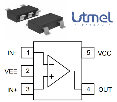
Pinout
TL331 CAD Model
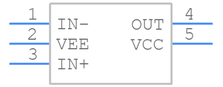
Symbol
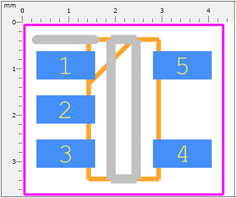
Footprint
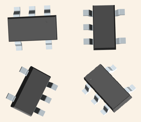
3D Model
TL331 Overview
The TL331 is an open collector, low−power comparator designed specifically to operate over a wide supply range from 2 V to 36 V single supply and ±1 V to ±18 V for split supplies. The input common−mode voltage range includes ground, even when operated from a single power supply voltage. TL331 comes in a space saving TSOP−5 package and is also available in an automotive qualified version.
This article provides you with a basic overview of the TL331, including its pin descriptions, features and specifications, etc., to help you quickly understand what TL331 is.
TL331 Features
● Wide Single Supply Voltage Range or Dual Supplies
● Low Supply Current: 0.5 mA Typical
● Low Input Bias Current: 25 nA Typical
● Low Input Offset Current: ±5 nA Typical
● Low Input Offset Voltage: ±2 mV Typical
● Input Common Mode Voltage Range includes Ground
● Low Output Saturation Voltage: 150 mV Typ at IO = 4 mA
● Differential Input Voltage Range Equal to the Supply Voltage
● TTL, DTL, ECL, CMOS Compatible Devices
● TL331V for Automotive and Other Applications Requiring Unique Site and Control Change Requirements; AEC−Q100 Qualified and PPAP Capable
● The Device is Pb−Free, Halogen Free/BFR Free and are RoHS Compliant
Specifications
- TypeParameter
- Lifecycle Status
Lifecycle Status refers to the current stage of an electronic component in its product life cycle, indicating whether it is active, obsolete, or transitioning between these states. An active status means the component is in production and available for purchase. An obsolete status indicates that the component is no longer being manufactured or supported, and manufacturers typically provide a limited time frame for support. Understanding the lifecycle status is crucial for design engineers to ensure continuity and reliability in their projects.
ACTIVE (Last Updated: 3 days ago) - Factory Lead Time11 Weeks
- Mounting Type
The "Mounting Type" in electronic components refers to the method used to attach or connect a component to a circuit board or other substrate, such as through-hole, surface-mount, or panel mount.
Surface Mount - Package / Case
refers to the protective housing that encases an electronic component, providing mechanical support, electrical connections, and thermal management.
SOT-23-5 Thin, TSOT-23-5 - Surface Mount
having leads that are designed to be soldered on the side of a circuit board that the body of the component is mounted on.
YES - Number of Pins5
- Number of Elements1
- Operating Temperature
The operating temperature is the range of ambient temperature within which a power supply, or any other electrical equipment, operate in. This ranges from a minimum operating temperature, to a peak or maximum operating temperature, outside which, the power supply may fail.
-40°C~125°C - Packaging
Semiconductor package is a carrier / shell used to contain and cover one or more semiconductor components or integrated circuits. The material of the shell can be metal, plastic, glass or ceramic.
Tape & Reel (TR) - Published2016
- JESD-609 Code
The "JESD-609 Code" in electronic components refers to a standardized marking code that indicates the lead-free solder composition and finish of electronic components for compliance with environmental regulations.
e3 - Pbfree Code
The "Pbfree Code" parameter in electronic components refers to the code or marking used to indicate that the component is lead-free. Lead (Pb) is a toxic substance that has been widely used in electronic components for many years, but due to environmental concerns, there has been a shift towards lead-free alternatives. The Pbfree Code helps manufacturers and users easily identify components that do not contain lead, ensuring compliance with regulations and promoting environmentally friendly practices. It is important to pay attention to the Pbfree Code when selecting electronic components to ensure they meet the necessary requirements for lead-free applications.
yes - Part Status
Parts can have many statuses as they progress through the configuration, analysis, review, and approval stages.
Active - Moisture Sensitivity Level (MSL)
Moisture Sensitivity Level (MSL) is a standardized rating that indicates the susceptibility of electronic components, particularly semiconductors, to moisture-induced damage during storage and the soldering process, defining the allowable exposure time to ambient conditions before they require special handling or baking to prevent failures
1 (Unlimited) - Number of Terminations5
- TypeGeneral Purpose
- Terminal Finish
Terminal Finish refers to the surface treatment applied to the terminals or leads of electronic components to enhance their performance and longevity. It can improve solderability, corrosion resistance, and overall reliability of the connection in electronic assemblies. Common finishes include nickel, gold, and tin, each possessing distinct properties suitable for various applications. The choice of terminal finish can significantly impact the durability and effectiveness of electronic devices.
Tin (Sn) - Terminal Position
In electronic components, the term "Terminal Position" refers to the physical location of the connection points on the component where external electrical connections can be made. These connection points, known as terminals, are typically used to attach wires, leads, or other components to the main body of the electronic component. The terminal position is important for ensuring proper connectivity and functionality of the component within a circuit. It is often specified in technical datasheets or component specifications to help designers and engineers understand how to properly integrate the component into their circuit designs.
DUAL - Terminal Form
Occurring at or forming the end of a series, succession, or the like; closing; concluding.
GULL WING - Peak Reflow Temperature (Cel)
Peak Reflow Temperature (Cel) is a parameter that specifies the maximum temperature at which an electronic component can be exposed during the reflow soldering process. Reflow soldering is a common method used to attach electronic components to a circuit board. The Peak Reflow Temperature is crucial because it ensures that the component is not damaged or degraded during the soldering process. Exceeding the specified Peak Reflow Temperature can lead to issues such as component failure, reduced performance, or even permanent damage to the component. It is important for manufacturers and assemblers to adhere to the recommended Peak Reflow Temperature to ensure the reliability and functionality of the electronic components.
NOT SPECIFIED - Number of Functions1
- Supply Voltage
Supply voltage refers to the electrical potential difference provided to an electronic component or circuit. It is crucial for the proper operation of devices, as it powers their functions and determines performance characteristics. The supply voltage must be within specified limits to ensure reliability and prevent damage to components. Different electronic devices have specific supply voltage requirements, which can vary widely depending on their design and intended application.
5V - Time@Peak Reflow Temperature-Max (s)
Time@Peak Reflow Temperature-Max (s) refers to the maximum duration that an electronic component can be exposed to the peak reflow temperature during the soldering process, which is crucial for ensuring reliable solder joint formation without damaging the component.
NOT SPECIFIED - Response Time
the time taken for a circuit or measuring device, when subjected to a change in input signal, to change its state by a specified fraction of its total response to that change.
850 ns - Voltage - Supply, Single/Dual (±)
The parameter "Voltage - Supply, Single/Dual (±)" in electronic components refers to the power supply voltage required for the proper operation of the component. This parameter indicates whether the component requires a single power supply voltage (e.g., 5V) or a dual power supply voltage (e.g., ±15V). For components that require a single power supply voltage, only one voltage level is needed for operation. On the other hand, components that require a dual power supply voltage need both positive and negative voltage levels to function correctly.Understanding the voltage supply requirements of electronic components is crucial for designing and integrating them into circuits to ensure proper functionality and prevent damage due to incorrect voltage levels.
2V~36V ±1V~18V - Average Bias Current-Max (IIB)
The parameter "Average Bias Current-Max (IIB)" in electronic components refers to the maximum average bias current that the component can handle without exceeding its specified operating limits. Bias current is the current that flows through a component when it is in its quiescent state or when it is not actively processing a signal. Exceeding the maximum average bias current can lead to overheating, reduced performance, or even damage to the component. Therefore, it is important to ensure that the bias current does not exceed the specified maximum value to maintain the reliability and longevity of the electronic component.
0.4μA - Current - Quiescent (Max)
The parameter "Current - Quiescent (Max)" in electronic components refers to the maximum amount of current that a device consumes when it is in a quiescent or idle state. This parameter is important because it indicates the minimum power consumption of the device when it is not actively performing any tasks. It is typically measured in units of amperes (A) and helps in determining the overall power efficiency and battery life of the electronic component. Designers and engineers use this parameter to ensure that the device meets power consumption requirements and operates within specified limits during standby or idle modes.
1.25mA - Voltage - Input Offset (Max)
Voltage - Input Offset (Max) is a parameter that refers to the maximum allowable difference in input voltage between two input terminals of an electronic component, such as an operational amplifier, before the output voltage deviates from the expected value. This parameter is crucial in precision applications where accurate voltage amplification or signal processing is required. A higher value for the input offset voltage indicates a greater potential for error in the output signal, so minimizing this parameter is important for maintaining the accuracy and reliability of the component's performance. Designers often take this parameter into consideration when selecting components for circuits that require precise voltage control and signal processing.
5mV @ 5V - Current - Input Bias (Max)
The parameter "Current - Input Bias (Max)" in electronic components refers to the maximum amount of input bias current that can flow into the input terminal of the component without causing any adverse effects on its performance. Input bias current is the small amount of current that flows into the input terminal of an electronic component, such as an operational amplifier, transistor, or integrated circuit, even when no input signal is applied. This parameter is important because excessive input bias current can lead to errors in the output signal and affect the overall performance of the component. Manufacturers specify a maximum value for input bias current to ensure proper operation and reliability of the component in various applications. It is crucial for designers and engineers to consider this parameter when selecting components for their circuits to ensure optimal performance and functionality.
250nA @ 5V - Current - Output (Typ)
The parameter "Current - Output (Typ)" in electronic components refers to the typical output current that the component is designed to deliver under normal operating conditions. It represents the expected or average value of the output current that the component can provide. This parameter is important for determining the capability of the component to supply power to other parts of the circuit or system. It helps in ensuring that the component can meet the current requirements of the application without exceeding its specified limits. Manufacturers provide this parameter in datasheets to help designers select the appropriate component for their specific needs.
16mA @ 5V - Propagation Delay (Max)
Propagation Delay (Max) is the maximum time it takes for a signal to travel through an electronic component, such as a logic gate or a flip-flop, from the input to the output. It is a critical specification in digital circuits since it determines how quickly the circuit can respond to input changes. High propagation delays can limit the operating speed of a circuit, affecting overall performance and timing. Understanding this parameter is essential for designing high-speed electronic systems.
850ns (Typ) - Length3mm
- RoHS Status
RoHS means “Restriction of Certain Hazardous Substances” in the “Hazardous Substances Directive” in electrical and electronic equipment.
ROHS3 Compliant
TL331 Functional Block Diagram
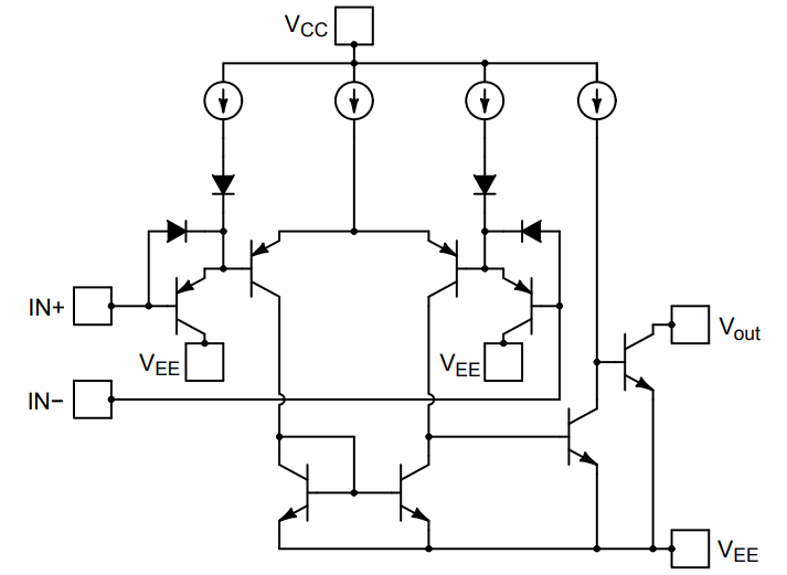
Functional Block Diagram
TL331 Marking Diagram
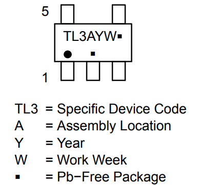
Marking Diagram
Parts with Similar Specs
- ImagePart NumberManufacturerPackage / CaseNumber of PinsSupply VoltageNumber of TerminationsBrand NameMoisture Sensitivity Level (MSL)LengthTerminal PositionView Compare
![TL331SN4T3G]()
TL331SN4T3G
SOT-23-5 Thin, TSOT-23-5
5
5 V
5
ON Semiconductor
1 (Unlimited)
3 mm
DUAL
![NCS2200SN2T1G]()
SOT-23-5 Thin, TSOT-23-5
5
3 V
5
ON Semiconductor
1 (Unlimited)
3 mm
DUAL
![TS391SN2T1G]()
SOT-23-5 Thin, TSOT-23-5
5
2.7 V
5
ON Semiconductor
1 (Unlimited)
3 mm
DUAL
![LMV331SN3T1G]()
SOT-23-5 Thin, TSOT-23-5
5
3 V
5
ON Semiconductor
1 (Unlimited)
3 mm
DUAL
![NCS2200SN1T1G]()
SOT-23-5 Thin, TSOT-23-5
5
5 V
5
ON Semiconductor
1 (Unlimited)
3 mm
DUAL

TL331 Typical Characteristics
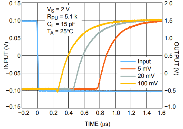
Low−to−High Propagation Delay vs. Overdrive at 2 V Supply
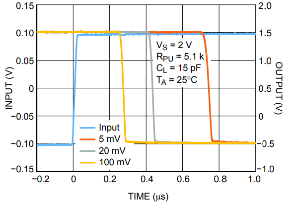
High−to−Low Propagation Delay vs. Overdrive at 2 V Supply
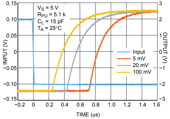
Low−to−High Propagation Delay vs. Overdrive at 5 V Supply
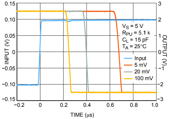
High−to−Low Propagation Delay vs. Overdrive at 5 V Supply
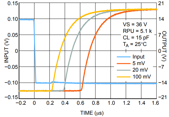
Low−to−High Propagation Delay vs. Overdrive at 36 V Supply
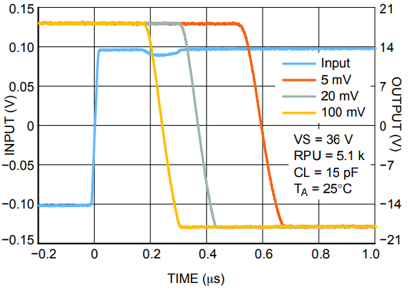
High−to−Low Propagation Delay vs. Overdrive at 36 V Supply
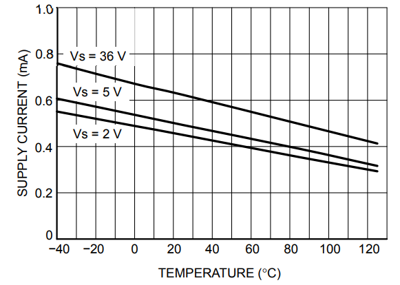
Quiescent Current vs. Temperature
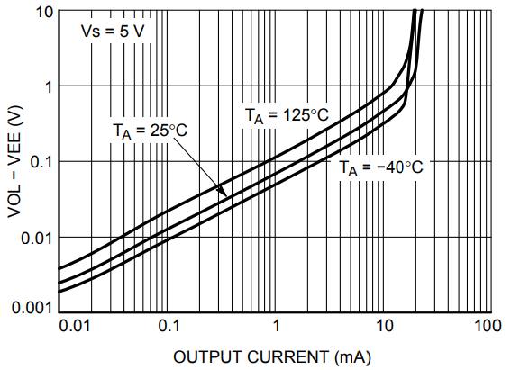
Low Level Output Voltage vs. Output Current at 5 V Supply
TL331 Package
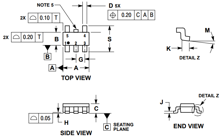
Package
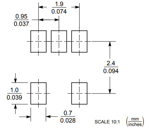
Soldering Footprint
TL331 Manufacturer
On Semiconductor (Nasdaq: ON) is a manufacturer engaging itself in reducing energy use. It features a comprehensive portfolio of power, signal management, and logic, custom solutions that are energy efficient. It acts as a world-class supply chain with high reliability and a network of manufacturing facilities, sales, offices, and design centers in key markets through North America, Europe, and the Asia Pacific regions.
Datasheet PDF
- PCN Assembly/Origin :
- ReachStatement :
- Datasheets :
- Environmental Information :
Trend Analysis
What is the essential property of the TL331?
The TL331 is an open collector, low−power comparator designed specifically to operate over a wide supply range from 2 V to 36 V single supply and ±1 V to ±18 V for split supplies.
What does the TL331 package look like?
TL331 comes in a space saving TSOP−5 package and is also available in an automotive qualified version.
 TPL5110DDCT Programmable Timer: Pinout, Layout, Datasheet
13 May 20213094
 rg6 vs rg11 Coaxials: What’s the Difference?
31 March 202258430
 CR2450 Battery: Datasheet, Equivalent, Features
22 July 202110609
 LTC6994IDCB-1#TRPBF Programmable Delay Line: Product Overview and Applications
06 March 2024257
 LM741CN vs UA741CN : Which one is better?
26 February 202210158
 Unveiling the Texas Instruments TMS470R1B768 Microcontroller
29 February 2024216
 PIC16F886 Microcontroller: Circuit, Pinout, and Datasheet
25 October 202113551
 Discovering the Microchip PIC32MX230F128HVMR Microcontroller: Architecture, Modules, and Guidelines
29 February 2024186
 A New Way of Thinking About the "Trolley Problem" of Artificial Intelligence
27 May 20221808
 Detecting Wafer Patterns using Semi-Supervised Learning
21 October 20221436
 Why is there a Chip Shortage?
19 October 20212832
 IOT-Based Anti-theft Handbag
29 August 20238172
 Schottky Diodes: Principle, Functions, and Applications
21 October 202527245
 Challenges in Enhancing Power Electronic Systems with Artificial Intelligence
26 December 20233222
 Chinese Chip Equipment Makers Thrive Amid US Restrictions
24 October 20232501
 Analysis of Wide Bandgap Devices in Renewable Energy Systems
11 April 20235233
ON Semiconductor
In Stock: 20
United States
China
Canada
Japan
Russia
Germany
United Kingdom
Singapore
Italy
Hong Kong(China)
Taiwan(China)
France
Korea
Mexico
Netherlands
Malaysia
Austria
Spain
Switzerland
Poland
Thailand
Vietnam
India
United Arab Emirates
Afghanistan
Åland Islands
Albania
Algeria
American Samoa
Andorra
Angola
Anguilla
Antigua & Barbuda
Argentina
Armenia
Aruba
Australia
Azerbaijan
Bahamas
Bahrain
Bangladesh
Barbados
Belarus
Belgium
Belize
Benin
Bermuda
Bhutan
Bolivia
Bonaire, Sint Eustatius and Saba
Bosnia & Herzegovina
Botswana
Brazil
British Indian Ocean Territory
British Virgin Islands
Brunei
Bulgaria
Burkina Faso
Burundi
Cabo Verde
Cambodia
Cameroon
Cayman Islands
Central African Republic
Chad
Chile
Christmas Island
Cocos (Keeling) Islands
Colombia
Comoros
Congo
Congo (DRC)
Cook Islands
Costa Rica
Côte d’Ivoire
Croatia
Cuba
Curaçao
Cyprus
Czechia
Denmark
Djibouti
Dominica
Dominican Republic
Ecuador
Egypt
El Salvador
Equatorial Guinea
Eritrea
Estonia
Eswatini
Ethiopia
Falkland Islands
Faroe Islands
Fiji
Finland
French Guiana
French Polynesia
Gabon
Gambia
Georgia
Ghana
Gibraltar
Greece
Greenland
Grenada
Guadeloupe
Guam
Guatemala
Guernsey
Guinea
Guinea-Bissau
Guyana
Haiti
Honduras
Hungary
Iceland
Indonesia
Iran
Iraq
Ireland
Isle of Man
Israel
Jamaica
Jersey
Jordan
Kazakhstan
Kenya
Kiribati
Kosovo
Kuwait
Kyrgyzstan
Laos
Latvia
Lebanon
Lesotho
Liberia
Libya
Liechtenstein
Lithuania
Luxembourg
Macao(China)
Madagascar
Malawi
Maldives
Mali
Malta
Marshall Islands
Martinique
Mauritania
Mauritius
Mayotte
Micronesia
Moldova
Monaco
Mongolia
Montenegro
Montserrat
Morocco
Mozambique
Myanmar
Namibia
Nauru
Nepal
New Caledonia
New Zealand
Nicaragua
Niger
Nigeria
Niue
Norfolk Island
North Korea
North Macedonia
Northern Mariana Islands
Norway
Oman
Pakistan
Palau
Palestinian Authority
Panama
Papua New Guinea
Paraguay
Peru
Philippines
Pitcairn Islands
Portugal
Puerto Rico
Qatar
Réunion
Romania
Rwanda
Samoa
San Marino
São Tomé & Príncipe
Saudi Arabia
Senegal
Serbia
Seychelles
Sierra Leone
Sint Maarten
Slovakia
Slovenia
Solomon Islands
Somalia
South Africa
South Sudan
Sri Lanka
St Helena, Ascension, Tristan da Cunha
St. Barthélemy
St. Kitts & Nevis
St. Lucia
St. Martin
St. Pierre & Miquelon
St. Vincent & Grenadines
Sudan
Suriname
Svalbard & Jan Mayen
Sweden
Syria
Tajikistan
Tanzania
Timor-Leste
Togo
Tokelau
Tonga
Trinidad & Tobago
Tunisia
Turkey
Turkmenistan
Turks & Caicos Islands
Tuvalu
U.S. Outlying Islands
U.S. Virgin Islands
Uganda
Ukraine
Uruguay
Uzbekistan
Vanuatu
Vatican City
Venezuela
Wallis & Futuna
Yemen
Zambia
Zimbabwe
![LM319MX]() LM319MX
LM319MXON Semiconductor
![LM393DR2G]() LM393DR2G
LM393DR2GON Semiconductor
![LM339DR2G]() LM339DR2G
LM339DR2GON Semiconductor
![LM239DR2G]() LM239DR2G
LM239DR2GON Semiconductor
![LM293DR2G]() LM293DR2G
LM293DR2GON Semiconductor
![LM393DMR2G]() LM393DMR2G
LM393DMR2GON Semiconductor
![LM2901DR2G]() LM2901DR2G
LM2901DR2GON Semiconductor
![LMV331SN3T1G]() LMV331SN3T1G
LMV331SN3T1GON Semiconductor
![LM2903DR2G]() LM2903DR2G
LM2903DR2GON Semiconductor
![LM2903DMR2G]() LM2903DMR2G
LM2903DMR2GON Semiconductor


