
 Product
 Brand
Brand Articles
 Tools
Tools
Xilinx XC2C512-10FT256I CPLD: Ultra-Low Power Design Solutions for Battery-Operated Embedded Systems


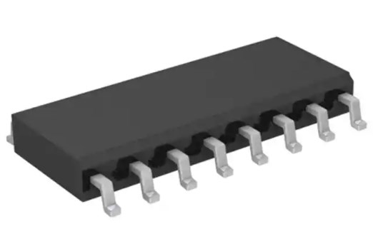
1mm PMIC CoolRunner II Series XC2C512 256 Pin 1.8V 256-LBGA
Learn how XC2C512-10FT256I enhances low power applications with Fast Zero Power technology, multi-voltage I/O, and efficient clock management for energy savings.
Product Introduction
When designing battery-operated devices, power efficiency becomes a top priority. The XC2C512-10FT256I stands out as a solution tailored for low power applications. Operating at a voltage as low as 1.8V, this device minimizes energy consumption without compromising performance. It draws a quiescent current of just 14 μA, which makes it perfect for handheld gadgets and communication systems. With support for mixed I/O voltages, it adapts seamlessly to various designs. These features ensure low power use, extending battery life in portable devices and reducing operational costs.
Understanding the XC2C512-10FT256I
Overview of the XC2C512-10FT256I
The XC2C512-10FT256I is a high-performance chip designed for embedded systems. It belongs to the CoolRunner-II family of CPLDs (Complex Programmable Logic Devices). This chip offers a balance of speed, power efficiency, and flexibility, making it ideal for modern applications. Its architecture is based on a 0.18-micron CMOS process, which ensures reliable performance and low power consumption. You can program it in-system using the IEEE 1532 (JTAG) interface, allowing quick and seamless updates.
This chip supports up to 512 macrocells and 212 I/O pins, providing ample resources for complex designs. Its multi-voltage I/O operation (1.5V to 3.3V) ensures compatibility with various systems. Additionally, the XC2C512-10FT256I includes advanced features like On-The-Fly Reconfiguration (OTF) and flexible clocking modes, which enhance its adaptability.
Relevance to Low Power Applications
If you’re working on battery-powered devices, the XC2C512-10FT256I is an excellent choice. Its low power design ensures minimal energy consumption, extending the battery life of portable devices. The chip operates at an internal voltage range of 1.7V to 1.9V, making it suitable for energy-sensitive applications. Its Fast Zero Power (FZP) technology further reduces standby power consumption, which is critical for devices that spend significant time in idle states.
The XC2C512-10FT256I also supports multiple I/O banks, allowing you to optimize power usage across different sections of your design. This feature is particularly useful in embedded systems where power efficiency is a priority.
Key Technical Specifications
Here’s a quick look at the technical specifications of the XC2C512-10FT256I:
| Specification | Value |
|---|---|
| Programmable Type | In System Programmable |
| Delay Time tpd(1) Max | 9.2ns |
| Voltage Supply - Internal | 1.7V ~ 1.9V |
| Number of Logic Elements/Blocks | 32 |
| Number of Macrocells | 512 |
| Number of Gates | 12000 |
| Number of I/O | 212 |
| Operating Temperature | -40℃ ~ 85℃ (TA) |
| Mounting Type | Surface Mount |
| Package / Case | 256-LBGA |
| Supplier Device Package | 256-FTBGA (17x17) |
These specifications highlight the chip’s versatility and suitability for a wide range of applications. Whether you’re designing IoT devices, wearable technology, or industrial automation systems, the XC2C512-10FT256I provides the performance and efficiency you need.
Features That Enable Low Power Usage
Fast Zero Power (FZP) Technology
Fast Zero Power (FZP) technology is one of the standout features of the XC2C512-10FT256I. This innovation minimizes power consumption during idle states, making it ideal for devices that spend significant time in standby mode. You’ll find this especially useful in battery-operated gadgets, where every microamp of current saved translates to extended battery life.
Key Benefits of FZP Technology:
Ultra-low standby power consumption, with currents as low as 14 µA.
Enhanced power efficiency for portable and battery-powered devices.
By leveraging FZP technology, you can design systems that remain energy-efficient without sacrificing performance. This feature ensures that your device stays ready to operate while consuming minimal power in standby mode.
Low Standby Power Consumption
The XC2C512-10FT256I excels in reducing standby power consumption, a critical factor for low power applications. Its architecture supports low voltage operation, which further reduces energy usage. This makes the chip an excellent choice for applications where power efficiency is a priority.
When your device enters standby mode, the programmable logic within the chip ensures that unnecessary operations are halted. This reduces energy waste and optimizes the overall power profile of your system. With in-system programmability, you can fine-tune the chip’s behavior to match your specific power-saving requirements.
Advanced Clocking Techniques
Efficient clock management plays a vital role in reducing power consumption, and the XC2C512-10FT256I incorporates advanced clocking techniques to achieve this. Resonant clocking, for example, reduces clocking power but struggles with frequency scaling. To overcome this, quasi-resonant clocking (QRC) offers a scalable solution, making it suitable for systems requiring voltage-frequency adjustments.
| Technique | Power Savings | Performance Drop |
|---|---|---|
| GALS | ~30% | 10% |
Globally Asynchronous Locally Synchronous (GALS) designs allow you to adjust frequency and voltage levels independently for each module. This flexibility enables dynamic voltage scaling (DVS), which can reduce energy consumption by up to 30%. Although there is a slight performance trade-off, the overall efficiency gains make it worthwhile for many low power applications.
By implementing these clocking techniques, you can optimize the logic operations within your system, ensuring that power is used only where it’s needed. This approach not only enhances efficiency but also extends the lifespan of your battery-powered devices.
Support for multiple I/O standards
The XC2C512-10FT256I offers robust support for multiple I/O standards, making it an adaptable choice for diverse applications. This feature allows you to integrate the chip into systems with varying voltage requirements and communication protocols. By supporting a wide range of I/O standards, the XC2C512-10FT256I ensures compatibility and flexibility in your designs.
Why Multiple I/O Standards Matter
When designing low power applications, you often need to connect components that operate at different voltage levels. For example, a microcontroller might use 3.3V logic, while a sensor operates at 1.8V. Without support for multiple I/O standards, you would need additional components like level shifters, which increase complexity and power consumption.
Tip: Using a chip with built-in support for multiple I/O standards simplifies your design and reduces energy usage.
The XC2C512-10FT256I eliminates the need for external level shifters by supporting I/O voltages ranging from 1.5V to 3.3V. This capability not only saves power but also reduces the overall size and cost of your system.
Key Benefits of Multi-Standard I/O Support
Here’s how this feature enhances your low power applications:
Seamless Integration: You can connect the chip to various components without worrying about voltage mismatches.
Reduced Power Consumption: Eliminating external level shifters minimizes energy loss.
Simplified Design: Fewer components mean a cleaner and more efficient circuit layout.
Enhanced Flexibility: The chip adapts to different systems, making it suitable for a wide range of applications.
Practical Example
Imagine you’re designing a wearable fitness tracker. The tracker includes a microcontroller, a heart rate sensor, and a Bluetooth module. Each component operates at a different voltage level. With the XC2C512-10FT256I, you can connect all these components directly to the chip. Its multi-standard I/O support ensures smooth communication between the components, reducing power consumption and extending battery life.
Technical Highlights
The XC2C512-10FT256I’s I/O banks allow you to configure different voltage levels for specific groups of pins. This feature is particularly useful in complex designs where multiple subsystems need to operate independently.
| Feature | Benefit |
|---|---|
| Multi-Voltage I/O Banks | Supports 1.5V, 1.8V, 2.5V, 3.3V |
| Configurable I/O Pins | Optimizes power usage |
| High-Speed Operation | Maintains performance |
By leveraging these capabilities, you can create efficient and reliable systems that meet the demands of modern low power applications.
Note: Always refer to the chip’s datasheet for detailed configuration options and guidelines.
The XC2C512-10FT256I’s support for multiple I/O standards is a game-changer for low power designs. It simplifies your work, reduces energy consumption, and ensures compatibility across various components. Whether you’re building IoT devices, portable electronics, or industrial systems, this feature provides the flexibility and efficiency you need.
Strategies for Optimizing Low Power Applications
Configuring Power-Saving Modes
Configuring power-saving modes is one of the most effective ways to reduce energy consumption in embedded systems. By transitioning your device between different power states, you can optimize its energy usage based on activity levels. The XC2C512-10FT256I supports multiple power modes, allowing you to tailor its behavior to your application's needs.
Power Mode Transitions
The chip enables smooth transitions between power modes, ensuring minimal disruption to system performance. Here’s a breakdown of common transitions:
| Power Mode Transition | Description |
|---|---|
| Active to Sleep | Reduces power consumption while keeping the system responsive. |
| Active to Deep Sleep | Further reduces power usage, suitable for longer idle periods. |
| Active to Hibernate | Lowest power state, ideal for extended periods of inactivity. |
These transitions allow you to balance energy efficiency with responsiveness. For example, switching to "Deep Sleep" during idle periods can significantly extend battery life without compromising functionality.
Practical Applications
You can configure power-saving modes for various devices, such as IoT sensors or wearable technology. For instance, a fitness tracker can enter "Sleep" mode when not in use and wake up instantly when a button is pressed. This approach minimizes energy waste while maintaining user convenience.
Case Studies
Here’s a table summarizing energy savings achieved by configuring power-saving modes in different applications:
| Control Strategy | Average Energy Savings | Payback Period |
|---|---|---|
| Schedule Timer | 48% | < 8 years |
| Kitchen Appliances | N/A | 0.7 years |
| Printer Rooms | N/A | 1.1 years |
| Miscellaneous Devices | N/A | 4.1 years |
| Workstations | N/A | 7.8 years |
These examples highlight the potential of power-saving modes to reduce energy consumption across diverse systems.
Tip: Use in-system programmability to fine-tune power modes for your specific application.
Efficient Clock Management
Clock management plays a crucial role in optimizing low power use. By controlling the clock signals within your system, you can reduce unnecessary logic operations and improve overall efficiency. The XC2C512-10FT256I incorporates advanced clocking techniques to help you achieve this.
Techniques for Clock Management
Here are some strategies you can implement:
Globally Asynchronous Locally Synchronous (GALS): Adjust frequency and voltage levels independently for each module. This technique reduces energy consumption by up to 30%.
Dynamic Voltage Scaling (DVS): Lower voltage levels during periods of reduced activity to save power.
| Technique | Power Savings | Performance Drop |
|---|---|---|
| GALS | ~30% | 10% |
These methods ensure that clock signals are used efficiently, minimizing energy waste while maintaining high performance.
Practical Example
Imagine you’re designing a smart thermostat. By implementing DVS, you can reduce the clock frequency during idle periods, saving energy without affecting the device’s responsiveness.
Note: Efficient clock management not only reduces power consumption but also extends the lifespan of your chip.
Leveraging Sleep and Standby States
Sleep and standby states are essential for low power applications. These states allow your device to conserve energy during idle periods while remaining ready to resume operation. The XC2C512-10FT256I supports multiple sleep modes, giving you flexibility in power management.
Types of Sleep States
The chip offers several sleep states, each tailored to different scenarios:
| Power Mode | Description |
|---|---|
| Low-Power (LP) | Reduces power consumption while maintaining performance. |
| Ultra-Low-Power (ULP) | Further reduces power consumption, ideal for battery-operated devices. |
| Deep Sleep | Minimizes power usage while allowing for quick wake-up. |
| Hibernate | Lowest power state, requires a full restart to resume operation. |
| Active | Normal operation mode with full performance. |
| Sleep | Low power state with some functionality still available. |
| Deep Sleep RAM | Retains RAM contents while in a low power state. |
Implementation Tips
Transition to "Ultra-Low-Power" mode during extended idle periods.
Use user buttons to wake the system from "Sleep" or "Deep Sleep" states.
Retain RAM contents in "Deep Sleep RAM" mode for faster recovery.
Real-World Benefits
Leveraging sleep states can significantly extend battery life in portable devices. For example, a wearable heart rate monitor can enter "Deep Sleep" mode when not actively measuring, conserving energy while remaining ready to wake up instantly.
Tip: Combine sleep states with efficient clock management for maximum energy savings.
Reducing unnecessary logic operations
Reducing unnecessary logic operations is a key strategy for optimizing low power applications. When your system performs fewer redundant tasks, it consumes less energy and operates more efficiently. By streamlining the logic within your design, you can achieve significant power savings without compromising functionality.
Why Reducing Logic Operations Matters
Every logic operation in your system requires power. Even small inefficiencies can add up, especially in devices that run continuously or rely on battery power. By minimizing unnecessary operations, you reduce the workload on the chip, which leads to lower energy consumption and improved performance.
For example, consider a wearable device that processes sensor data. If the device performs redundant calculations or checks, it wastes valuable energy. By optimizing the logic, you ensure that only essential operations are executed, extending the device's battery life.
Practical Techniques for Optimization
Here are some practical ways to reduce unnecessary logic operations in your designs:
Simplify Boolean Expressions
Simplifying Boolean expressions in your code can eliminate redundant logic gates. For instance, using Karnaugh maps or other simplification techniques can help you identify and remove unnecessary terms.Use Conditional Execution
Implement conditional execution to bypass operations that are not needed. For example, instead of running a calculation every cycle, you can set conditions to execute it only when required.Optimize Data Paths
Streamline data paths to reduce the number of logic gates involved in processing. This can be achieved by reordering operations or combining multiple steps into one.Leverage Built-in Features
The XC2C512-10FT256I includes features like On-The-Fly Reconfiguration (OTF), which allows you to dynamically adjust the logic based on current needs. By using this feature, you can deactivate unused sections of the chip, saving power.
Evidence of Efficiency Gains
Studies have shown that reducing unnecessary logic operations can lead to measurable improvements in power efficiency. The table below highlights the impact of optimization on logical errors and relative error reduction:
| Code Type | Logical Error per Cycle (%) | Relative Error Reduction (%) |
|---|---|---|
| Distance-5 | 2.914 ± 0.016 | 4% |
| Distance-3 Avg | 3.028 ± 0.023 | N/A |
| Distance-5 (faster decoder) | 3.056 ± 0.015 | 2% |
| Distance-3 (faster decoder) | 3.118 ± 0.025 | N/A |
This data demonstrates how optimizing logic operations can reduce errors and improve overall system performance. While the percentage reductions may seem small, they translate to significant energy savings in large-scale or long-term applications.
Real-World Example
Imagine you are designing an IoT sensor that monitors temperature. The sensor collects data every second, but the environment changes slowly. Instead of processing every data point, you can implement logic to analyze only significant changes. This approach reduces the number of operations, conserving energy while maintaining accuracy.
Tip: Regularly review your design to identify and eliminate redundant logic operations. Small adjustments can lead to big improvements in power efficiency.
By focusing on reducing unnecessary logic operations, you can create systems that are not only energy-efficient but also more reliable and cost-effective. This strategy is essential for modern low power applications, where every microamp of current saved makes a difference.
Real-World Applications of XC2C512-10FT256I
IoT Devices and Sensors
The XC2C512-10FT256I is a perfect fit for IoT devices and sensors. Its low power design ensures efficient energy use, which is critical for devices that operate continuously or rely on batteries. You can use this chip in smart home systems, environmental monitoring sensors, and industrial IoT setups. Its ability to handle multiple I/O standards allows seamless integration with various components, making it versatile for different applications.
For example, in a smart home, the chip can manage communication between temperature sensors, motion detectors, and control hubs. Its low standby power consumption ensures that these devices remain operational for extended periods without frequent battery replacements. Additionally, the chip’s compact design makes it suitable for space-constrained IoT devices, such as wireless sensors or compact gateways.
Wearable Technology
Wearable devices like fitness trackers and smartwatches demand compact, energy-efficient components. The XC2C512-10FT256I meets these requirements with its small 256-ball LBGA package and low power consumption. You can rely on this chip to manage control logic and sensor interfacing, which are essential for wearable technology.
For instance, in a smartwatch, the chip can process data from accelerometers, heart rate monitors, and GPS modules. Its ability to operate at low voltages reduces overall power consumption, extending the device’s battery life. The chip’s reprogrammable nature also allows you to update features or fix bugs without replacing hardware, ensuring long-term usability.
Battery-Powered Portable Electronics
Portable electronics, such as barcode scanners and GPS units, benefit greatly from the XC2C512-10FT256I’s features. Its high macrocell count supports complex logic designs, while its low voltage operation minimizes energy use. These characteristics make it an excellent choice for devices that prioritize efficiency and reliability.
For example, in a barcode scanner, the chip can handle signal processing and communication with minimal power draw. Its reliable performance across a wide temperature range ensures consistent operation in various environments. Additionally, the chip’s compact design saves space, allowing you to create smaller, more portable devices.
Tip: By using the XC2C512-10FT256I in your designs, you can achieve a balance between performance and energy efficiency, making it ideal for modern low power applications.
Industrial automation systems
Industrial automation systems rely on efficient and reliable components to ensure smooth operations. The XC2C512-10FT256I offers features that make it an excellent choice for these systems. Its low power consumption, high performance, and flexibility allow you to design automation solutions that are both cost-effective and energy-efficient.
Why Choose XC2C512-10FT256I for Automation?
You can use the XC2C512-10FT256I to manage complex control logic in industrial environments. Its ability to operate at low voltages reduces energy costs, which is critical for systems running 24/7. The chip’s support for multiple I/O standards ensures compatibility with various sensors, actuators, and communication protocols.
Tip: Use the chip’s in-system programmability to update control logic without halting operations. This feature minimizes downtime and boosts productivity.
Practical Applications in Automation
Here are some ways you can integrate the XC2C512-10FT256I into industrial automation:
Robotic Arms: Control precise movements with minimal power usage.
Conveyor Systems: Manage speed and direction efficiently.
Monitoring Equipment: Process sensor data in real-time for better decision-making.
Key Benefits for Industrial Use
| Feature | Benefit |
|---|---|
| Low Power Consumption | Reduces operational costs |
| High Macrocell Count | Handles complex logic designs |
| Wide Temperature Range | Operates reliably in harsh environments |
By leveraging these features, you can create robust automation systems that meet modern industry demands. The XC2C512-10FT256I ensures your designs are efficient, reliable, and future-proof.
Note: Always test your designs in real-world conditions to ensure optimal performance.
Benefits and Challenges in Low Power Scenarios
Advantages of using XC2C512-10FT256I
The XC2C512-10FT256I offers several advantages for low power applications. Its Fast Zero Power (FZP) technology ensures minimal energy consumption during idle states. This feature is especially useful for devices that spend significant time in standby mode. The chip’s low standby power consumption extends battery life, making it ideal for portable electronics and IoT devices.
You can also benefit from its support for multiple I/O standards. This flexibility allows seamless integration into systems with varying voltage requirements. Additionally, the chip’s programmable nature enables you to customize its logic to meet specific application needs. Its compact design and high macrocell count make it suitable for space-constrained designs that require complex control logic.
Potential limitations and considerations
While the XC2C512-10FT256I excels in many areas, you should consider a few limitations. Its commercial temperature range may not perform well in harsh environments. If your application requires extreme temperature tolerance, this chip might not be the best choice.
The high pin count can also pose challenges during the design phase. You may need extra effort to manage the connections effectively. Furthermore, the XC2C512-10FT256I is not as widely adopted as larger FPGAs. This could mean fewer tools and limited support compared to more popular programmable logic devices.
Comparison with alternative CPLD solutions
When compared to other CPLD solutions, the XC2C512-10FT256I stands out for its low power consumption and advanced features. Many CPLDs lack the Fast Zero Power (FZP) technology, which gives this chip an edge in energy efficiency. Its ability to support multiple I/O standards also sets it apart, as not all CPLDs offer this level of flexibility.
However, larger FPGAs may provide more resources for highly complex systems. If your application requires extensive logic or operates in extreme conditions, an FPGA might be a better fit. Despite this, the XC2C512-10FT256I remains a strong contender for low power applications that prioritize efficiency and compact design.
The XC2C512-10FT256I offers a powerful solution for low power applications. Its optimized 1.8V operation, Fast Zero Power (FZP) technology, and multi-voltage I/O compatibility make it ideal for energy-efficient designs. You can enhance performance by leveraging features like advanced clocking and power-saving modes.
| Feature | Description |
|---|---|
| Operating Voltage | Optimized for 1.8V systems |
| Power Efficiency | Industry’s fastest low power CPLD |
| Macrocell Density | Densities from 32 to 512 macrocells |
| CMOS Technology | Industry’s best 0.18 micron CMOS CPLD |
Explore its potential to create innovative, low power designs that maximize efficiency and reliability.
FAQ
1. What makes the XC2C512-10FT256I ideal for low power applications?
The XC2C512-10FT256I uses Fast Zero Power (FZP) technology, which minimizes power consumption during idle states. Its low standby power and support for multiple I/O standards make it perfect for energy-efficient designs like IoT devices and portable electronics.
2. Can you program the XC2C512-10FT256I in-system?
Yes, you can program it in-system using the IEEE 1532 (JTAG) interface. This feature allows you to update or reconfigure the chip without removing it from the device, saving time and effort.
3. How does the chip handle multiple voltage levels?
The XC2C512-10FT256I supports multi-voltage I/O banks, allowing you to connect components with different voltage requirements. This eliminates the need for external level shifters, simplifying your design and reducing power consumption.
4. Is the XC2C512-10FT256I suitable for wearable devices?
Absolutely! Its compact size, low power consumption, and ability to operate at low voltages make it an excellent choice for wearable technology like fitness trackers and smartwatches.
5. What are the temperature limits for the XC2C512-10FT256I?
The chip operates reliably within a temperature range of -40°C to 85°C. This makes it suitable for most consumer and industrial applications, though it may not perform well in extreme environments.
Tip: Always check the datasheet for detailed specifications before integrating the chip into your design.
Specifications
- TypeParameter
- Factory Lead Time10 Weeks
- Mount
In electronic components, the term "Mount" typically refers to the method or process of physically attaching or fixing a component onto a circuit board or other electronic device. This can involve soldering, adhesive bonding, or other techniques to secure the component in place. The mounting process is crucial for ensuring proper electrical connections and mechanical stability within the electronic system. Different components may have specific mounting requirements based on their size, shape, and function, and manufacturers provide guidelines for proper mounting procedures to ensure optimal performance and reliability of the electronic device.
Surface Mount - Mounting Type
The "Mounting Type" in electronic components refers to the method used to attach or connect a component to a circuit board or other substrate, such as through-hole, surface-mount, or panel mount.
Surface Mount - Package / Case
refers to the protective housing that encases an electronic component, providing mechanical support, electrical connections, and thermal management.
256-LBGA - Number of Pins256
- Number of I/Os212
- Operating Temperature
The operating temperature is the range of ambient temperature within which a power supply, or any other electrical equipment, operate in. This ranges from a minimum operating temperature, to a peak or maximum operating temperature, outside which, the power supply may fail.
-40°C~85°C TA - Packaging
Semiconductor package is a carrier / shell used to contain and cover one or more semiconductor components or integrated circuits. The material of the shell can be metal, plastic, glass or ceramic.
Tray - Series
In electronic components, the "Series" refers to a group of products that share similar characteristics, designs, or functionalities, often produced by the same manufacturer. These components within a series typically have common specifications but may vary in terms of voltage, power, or packaging to meet different application needs. The series name helps identify and differentiate between various product lines within a manufacturer's catalog.
CoolRunner II - Published1997
- JESD-609 Code
The "JESD-609 Code" in electronic components refers to a standardized marking code that indicates the lead-free solder composition and finish of electronic components for compliance with environmental regulations.
e0 - Pbfree Code
The "Pbfree Code" parameter in electronic components refers to the code or marking used to indicate that the component is lead-free. Lead (Pb) is a toxic substance that has been widely used in electronic components for many years, but due to environmental concerns, there has been a shift towards lead-free alternatives. The Pbfree Code helps manufacturers and users easily identify components that do not contain lead, ensuring compliance with regulations and promoting environmentally friendly practices. It is important to pay attention to the Pbfree Code when selecting electronic components to ensure they meet the necessary requirements for lead-free applications.
no - Part Status
Parts can have many statuses as they progress through the configuration, analysis, review, and approval stages.
Active - Moisture Sensitivity Level (MSL)
Moisture Sensitivity Level (MSL) is a standardized rating that indicates the susceptibility of electronic components, particularly semiconductors, to moisture-induced damage during storage and the soldering process, defining the allowable exposure time to ambient conditions before they require special handling or baking to prevent failures
3 (168 Hours) - Number of Terminations256
- ECCN Code
An ECCN (Export Control Classification Number) is an alphanumeric code used by the U.S. Bureau of Industry and Security to identify and categorize electronic components and other dual-use items that may require an export license based on their technical characteristics and potential for military use.
3A991.D - Terminal Finish
Terminal Finish refers to the surface treatment applied to the terminals or leads of electronic components to enhance their performance and longevity. It can improve solderability, corrosion resistance, and overall reliability of the connection in electronic assemblies. Common finishes include nickel, gold, and tin, each possessing distinct properties suitable for various applications. The choice of terminal finish can significantly impact the durability and effectiveness of electronic devices.
Tin/Lead (Sn63Pb37) - Additional Feature
Any Feature, including a modified Existing Feature, that is not an Existing Feature.
YES - HTS Code
HTS (Harmonized Tariff Schedule) codes are product classification codes between 8-1 digits. The first six digits are an HS code, and the countries of import assign the subsequent digits to provide additional classification. U.S. HTS codes are 1 digits and are administered by the U.S. International Trade Commission.
8542.39.00.01 - Terminal Position
In electronic components, the term "Terminal Position" refers to the physical location of the connection points on the component where external electrical connections can be made. These connection points, known as terminals, are typically used to attach wires, leads, or other components to the main body of the electronic component. The terminal position is important for ensuring proper connectivity and functionality of the component within a circuit. It is often specified in technical datasheets or component specifications to help designers and engineers understand how to properly integrate the component into their circuit designs.
BOTTOM - Terminal Form
Occurring at or forming the end of a series, succession, or the like; closing; concluding.
BALL - Peak Reflow Temperature (Cel)
Peak Reflow Temperature (Cel) is a parameter that specifies the maximum temperature at which an electronic component can be exposed during the reflow soldering process. Reflow soldering is a common method used to attach electronic components to a circuit board. The Peak Reflow Temperature is crucial because it ensures that the component is not damaged or degraded during the soldering process. Exceeding the specified Peak Reflow Temperature can lead to issues such as component failure, reduced performance, or even permanent damage to the component. It is important for manufacturers and assemblers to adhere to the recommended Peak Reflow Temperature to ensure the reliability and functionality of the electronic components.
240 - Supply Voltage
Supply voltage refers to the electrical potential difference provided to an electronic component or circuit. It is crucial for the proper operation of devices, as it powers their functions and determines performance characteristics. The supply voltage must be within specified limits to ensure reliability and prevent damage to components. Different electronic devices have specific supply voltage requirements, which can vary widely depending on their design and intended application.
1.8V - Terminal Pitch
The center distance from one pole to the next.
1mm - Time@Peak Reflow Temperature-Max (s)
Time@Peak Reflow Temperature-Max (s) refers to the maximum duration that an electronic component can be exposed to the peak reflow temperature during the soldering process, which is crucial for ensuring reliable solder joint formation without damaging the component.
30 - Base Part Number
The "Base Part Number" (BPN) in electronic components serves a similar purpose to the "Base Product Number." It refers to the primary identifier for a component that captures the essential characteristics shared by a group of similar components. The BPN provides a fundamental way to reference a family or series of components without specifying all the variations and specific details.
XC2C512 - Pin Count
a count of all of the component leads (or pins)
256 - Qualification Status
An indicator of formal certification of qualifications.
Not Qualified - Operating Supply Voltage
The voltage level by which an electrical system is designated and to which certain operating characteristics of the system are related.
1.8V - Supply Voltage-Max (Vsup)
The parameter "Supply Voltage-Max (Vsup)" in electronic components refers to the maximum voltage that can be safely applied to the component without causing damage. It is an important specification to consider when designing or using electronic circuits to ensure the component operates within its safe operating limits. Exceeding the maximum supply voltage can lead to overheating, component failure, or even permanent damage. It is crucial to adhere to the specified maximum supply voltage to ensure the reliable and safe operation of the electronic component.
1.9V - Programmable Type
These include Field Programmable Logic Devices (FPGAs), Complex Programmable Logic Devices (CPLD) and Programmable Logic Devices (PLD, PLA, PAL, GAL). There are also devices that are the analog equivalent of these called field programmable analog arrays.
In System Programmable - Propagation Delay
the flight time of packets over the transmission link and is limited by the speed of light.
10 ns - Number of Logic Elements/Cells32
- Number of Gates
The number of gates per IC varies depending on the number of inputs per gate. Two?input gates are common, but if only a single input is required, such as in the 744 NOT(or inverter) gates, a 14 pin IC can accommodate 6 (or Hex) gates.
12000 - Max Frequency
Max Frequency refers to the highest frequency at which an electronic component can operate effectively without degradation of performance. It is a critical parameter for devices such as transistors, capacitors, and oscillators, indicating their limitations in speed and response time. Exceeding the max frequency can lead to issues like signal distortion, heat generation, and potential failure of the component. Understanding this parameter is essential for designing circuits to ensure reliable and efficient operation.
128MHz - Speed Grade
Speed grade is a specification in electronic components that indicates the maximum operating speed at which the component can reliably function. It is commonly used for integrated circuits, particularly in digital logic devices and programmable logic devices. The speed grade is typically denoted by a number or letter code that correlates to the maximum frequency or propagation delay of the device, influencing its performance in high-speed applications. Components with higher speed grades are capable of faster processing and lower signal delay compared to those with lower grades.
10 - Output Function
An output function is a function that an optimization function calls at each iteration of its algorithm. Typically, you use an output function to generate graphical output, record the history of the data the algorithm generates, or halt the algorithm based on the data at the current iteration.
MACROCELL - Number of Macro Cells512
- JTAG BST
JTAG BST stands for Joint Test Action Group Boundary Scan Test. It is a testing technique used in electronic components to verify the functionality of integrated circuits on a printed circuit board. The JTAG BST method allows for testing of individual components without the need for physical access to the pins of the component, making it a valuable tool for debugging and testing complex electronic systems. By using a standardized test access port and a set of test logic, JTAG BST can help identify faults, shorts, and other issues in electronic components quickly and efficiently.
YES - Voltage Supply - Internal
Voltage Supply - Internal is a parameter in electronic components that refers to the internal voltage supply required for the proper functioning of the component. This voltage supply is typically generated within the component itself and is used to power its internal circuitry. It is important for the component to receive the correct internal voltage supply to ensure reliable operation and performance. The specified voltage supply range for a component must be adhered to in order to prevent damage or malfunction. Manufacturers provide this information in the component's datasheet to guide users in proper integration and usage.
1.7V~1.9V - Delay Time tpd(1) Max
The parameter "Delay Time tpd(1) Max" in electronic components refers to the maximum time delay between the input signal changing and the output signal responding. It represents the longest time it takes for the output to change after a change in the input signal. This parameter is crucial in determining the speed and performance of the component in various electronic circuits. A longer delay time can result in slower response times and potentially impact the overall functionality of the circuit. It is important to consider this parameter when designing or selecting electronic components to ensure proper operation and timing requirements are met.
9.2ns - Length17mm
- Height Seated (Max)
Height Seated (Max) is a parameter in electronic components that refers to the maximum allowable height of the component when it is properly seated or installed on a circuit board or within an enclosure. This specification is crucial for ensuring proper fit and alignment within the overall system design. Exceeding the maximum seated height can lead to mechanical interference, electrical shorts, or other issues that may impact the performance and reliability of the electronic device. Manufacturers provide this information to help designers and engineers select components that will fit within the designated space and function correctly in the intended application.
1.55mm - Width17mm
- RoHS Status
RoHS means “Restriction of Certain Hazardous Substances” in the “Hazardous Substances Directive” in electrical and electronic equipment.
Non-RoHS Compliant
Parts with Similar Specs
- ImagePart NumberManufacturerPackage / CaseNumber of PinsPropagation DelayNumber of Macro CellsNumber of I/OMax FrequencySupply VoltageNumber of TerminationsView Compare
![XC2C512-10FT256I]()
XC2C512-10FT256I
256-LBGA
256
10 ns
512
212
128 MHz
1.8 V
256
![LC4512V-10FTN256I]()
256-LBGA
256
10 ns
512
208
-
3.3 V
256
![XCR3512XL-10FTG256C]()
BGA
256
10 ns
512
212
-
2.5 V
256
![XCR3512XL-10FTG256I]()
256-LBGA
256
10 ns
512
212
97 MHz
3.3 V
256


Datasheet PDF
- Design Resources :
- Datasheets :
 TS5V330D Video Switch: Pinout, Features and Specification
14 August 2024957
![The Overview of MS5637 Pressure Sensor [Video]](https://res.utmel.com/Images/Article/03e2393d-b9f4-4c6b-ba73-6857e5ea7a29.jpg) The Overview of MS5637 Pressure Sensor [Video]
The Overview of MS5637 Pressure Sensor [Video]08 July 20211035
 BC546 NPN Transistor: Equivalents, Datasheet, and Pinout
05 August 202116261
 TM1650 LED Drive Control: Datasheet pdf, Circuit and Pinout
16 November 202118617
 CD4543BE: Datasheet, Circuit, and Pinout
06 August 20215199
![TMC2100 Stepper Motor Driver[Video]: TMC2100 VS TMC2130 VS TMC2208, Pinout, and Datasheet](https://res.utmel.com/Images/Article/e7efba4d-e32d-4aad-a44e-9aaf2ff650e2.png) TMC2100 Stepper Motor Driver[Video]: TMC2100 VS TMC2130 VS TMC2208, Pinout, and Datasheet
TMC2100 Stepper Motor Driver[Video]: TMC2100 VS TMC2130 VS TMC2208, Pinout, and Datasheet05 May 20225994
 UA741IN OP AMP: Feature, Specification, and Datasheet
10 June 20213529
 LM6172 Voltage Feedback Amplifier: Pinout, Application and Datasheet
17 November 20212761
 What is Bluetooth Low Energy (BLE) Audio Technology?
26 April 20227008
 Analog-to-Digital Converters (ADCs): Decrypting Resolutions and Sampling Rates
24 February 20225344
 What is a Fixed Inductor?
15 April 202113210
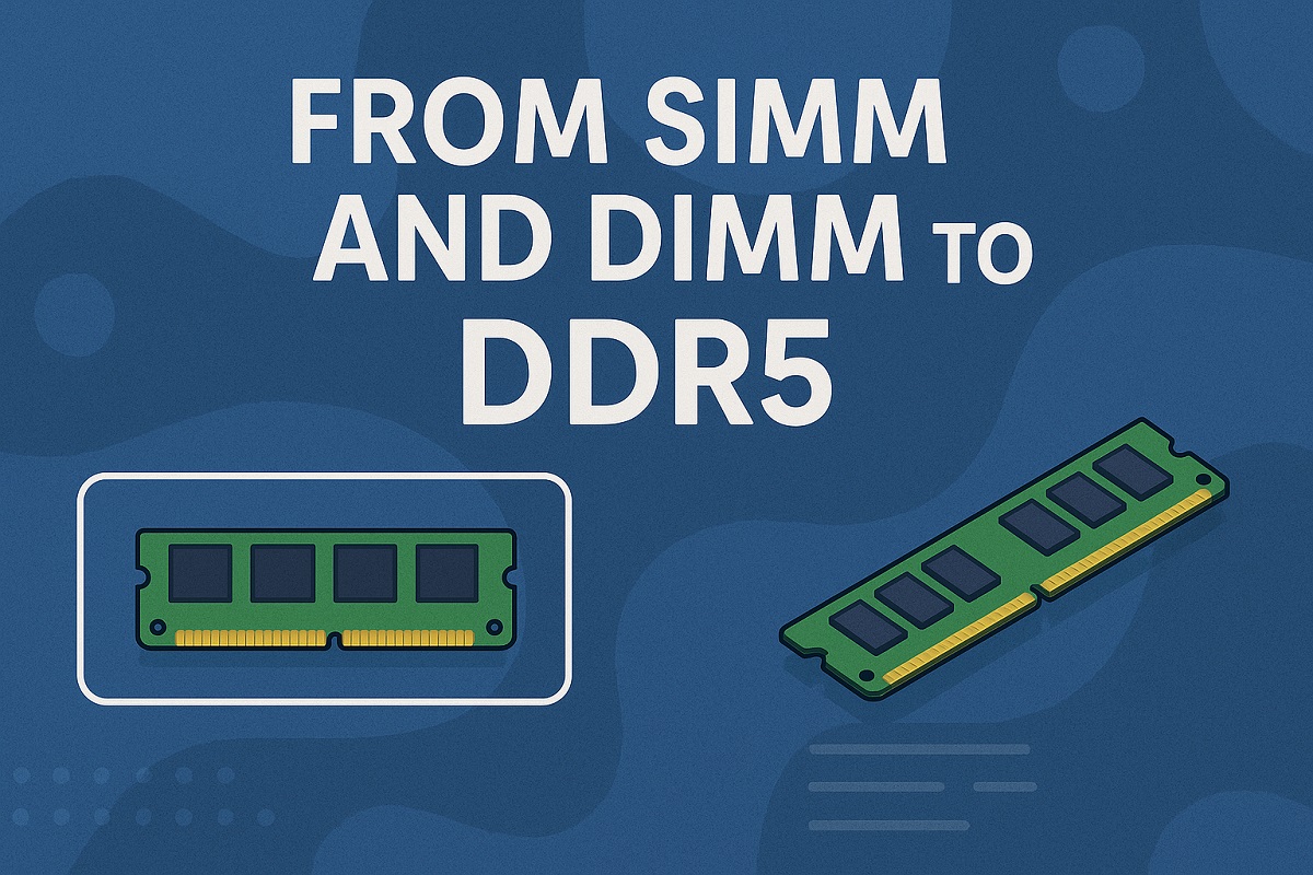 Understanding Computer Memory: From SIMM and DIMM to DDR5
23 May 202521778
 Introduction to Temperature Sensors
24 October 202510163
 What are Proximity Sensors?
24 October 20258432
 What's the Difference Between Operational Amplifier and Comparator?
01 April 20226239
 What is Chip: Definition, Classification and Design Process
17 January 20267033
Xilinx Inc.
In Stock: 5
United States
China
Canada
Japan
Russia
Germany
United Kingdom
Singapore
Italy
Hong Kong(China)
Taiwan(China)
France
Korea
Mexico
Netherlands
Malaysia
Austria
Spain
Switzerland
Poland
Thailand
Vietnam
India
United Arab Emirates
Afghanistan
Åland Islands
Albania
Algeria
American Samoa
Andorra
Angola
Anguilla
Antigua & Barbuda
Argentina
Armenia
Aruba
Australia
Azerbaijan
Bahamas
Bahrain
Bangladesh
Barbados
Belarus
Belgium
Belize
Benin
Bermuda
Bhutan
Bolivia
Bonaire, Sint Eustatius and Saba
Bosnia & Herzegovina
Botswana
Brazil
British Indian Ocean Territory
British Virgin Islands
Brunei
Bulgaria
Burkina Faso
Burundi
Cabo Verde
Cambodia
Cameroon
Cayman Islands
Central African Republic
Chad
Chile
Christmas Island
Cocos (Keeling) Islands
Colombia
Comoros
Congo
Congo (DRC)
Cook Islands
Costa Rica
Côte d’Ivoire
Croatia
Cuba
Curaçao
Cyprus
Czechia
Denmark
Djibouti
Dominica
Dominican Republic
Ecuador
Egypt
El Salvador
Equatorial Guinea
Eritrea
Estonia
Eswatini
Ethiopia
Falkland Islands
Faroe Islands
Fiji
Finland
French Guiana
French Polynesia
Gabon
Gambia
Georgia
Ghana
Gibraltar
Greece
Greenland
Grenada
Guadeloupe
Guam
Guatemala
Guernsey
Guinea
Guinea-Bissau
Guyana
Haiti
Honduras
Hungary
Iceland
Indonesia
Iran
Iraq
Ireland
Isle of Man
Israel
Jamaica
Jersey
Jordan
Kazakhstan
Kenya
Kiribati
Kosovo
Kuwait
Kyrgyzstan
Laos
Latvia
Lebanon
Lesotho
Liberia
Libya
Liechtenstein
Lithuania
Luxembourg
Macao(China)
Madagascar
Malawi
Maldives
Mali
Malta
Marshall Islands
Martinique
Mauritania
Mauritius
Mayotte
Micronesia
Moldova
Monaco
Mongolia
Montenegro
Montserrat
Morocco
Mozambique
Myanmar
Namibia
Nauru
Nepal
New Caledonia
New Zealand
Nicaragua
Niger
Nigeria
Niue
Norfolk Island
North Korea
North Macedonia
Northern Mariana Islands
Norway
Oman
Pakistan
Palau
Palestinian Authority
Panama
Papua New Guinea
Paraguay
Peru
Philippines
Pitcairn Islands
Portugal
Puerto Rico
Qatar
Réunion
Romania
Rwanda
Samoa
San Marino
São Tomé & Príncipe
Saudi Arabia
Senegal
Serbia
Seychelles
Sierra Leone
Sint Maarten
Slovakia
Slovenia
Solomon Islands
Somalia
South Africa
South Sudan
Sri Lanka
St Helena, Ascension, Tristan da Cunha
St. Barthélemy
St. Kitts & Nevis
St. Lucia
St. Martin
St. Pierre & Miquelon
St. Vincent & Grenadines
Sudan
Suriname
Svalbard & Jan Mayen
Sweden
Syria
Tajikistan
Tanzania
Timor-Leste
Togo
Tokelau
Tonga
Trinidad & Tobago
Tunisia
Turkey
Turkmenistan
Turks & Caicos Islands
Tuvalu
U.S. Outlying Islands
U.S. Virgin Islands
Uganda
Ukraine
Uruguay
Uzbekistan
Vanuatu
Vatican City
Venezuela
Wallis & Futuna
Yemen
Zambia
Zimbabwe
![XC95144XL-10TQG144C]() XC95144XL-10TQG144C
XC95144XL-10TQG144CXilinx Inc.
![XC9572XL-10VQG44I]() XC9572XL-10VQG44I
XC9572XL-10VQG44IXilinx Inc.
![XC9572XL-10VQG44C]() XC9572XL-10VQG44C
XC9572XL-10VQG44CXilinx Inc.
![XC9572XL-10TQG100C]() XC9572XL-10TQG100C
XC9572XL-10TQG100CXilinx Inc.
![XC9572XL-10VQG64C]() XC9572XL-10VQG64C
XC9572XL-10VQG64CXilinx Inc.
![XC9572XL-10TQG100I]() XC9572XL-10TQG100I
XC9572XL-10TQG100IXilinx Inc.
![XC2C128-7VQG100C]() XC2C128-7VQG100C
XC2C128-7VQG100CXilinx Inc.
![XC2C64A-7QFG48C]() XC2C64A-7QFG48C
XC2C64A-7QFG48CXilinx Inc.
![XC95144XL-7TQ100C]() XC95144XL-7TQ100C
XC95144XL-7TQ100CXilinx Inc.
![XC2C256-7VQG100C]() XC2C256-7VQG100C
XC2C256-7VQG100CXilinx Inc.


