
 Product
 Brand
Brand Articles
 Tools
Tools
TPS22918DBVR On-Resistance Load Switch: Layout, Pinout, and Datasheet


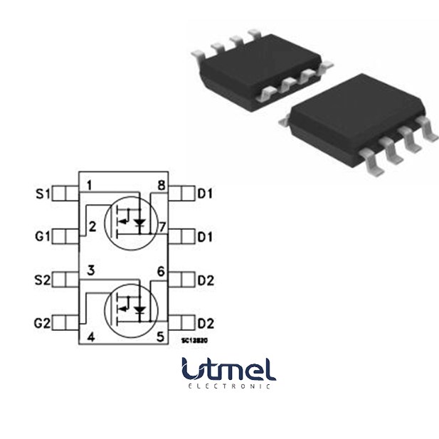
N-Channel 0.95mm PMIC TPS22918 6 Pin 1V SOT-23-6
The TPS22918DBVR is a single-channel load switch with the adjustable rise and short output discharge times. This article mainly introduces Layout, Pinout, Datasheet and other detailed information about Texas Instruments TPS22918DBVR.

Episode 10: Load Switches Ahead
- TPS22918DBVR Description
- TPS22918DBVR Pinout
- TPS22918DBVR CAD Model
- TPS22918DBVR Features
- Specifications
- Parts with Similar Specs
- TPS22918DBVR Functional Block Diagram
- TPS22918DBVR Typical Application
- TPS22918DBVR Simplified Schematic
- TPS22918DBVR Layout
- TPS22918DBVR Alternatives
- TPS22918DBVR Applications
- TPS22918DBVR Package
- TPS22918DBVR Manufacturer
- Trend Analysis
- Datasheet PDF
TPS22918DBVR Description
The TPS22918DBVR is a single-channel load switch with the adjustable rise and short output discharge times. An N-channel MOSFET is included in the device, which can function between 1 and 5.5 V and handle a maximum continuous current of 2 A. The switch is operated via an on/off input that can interface with low-voltage control signals directly.
The device's adjustable rise time minimizes inrush current induced by large bulk load capacitances, decreasing or eliminating power supply droop. The TPS22918DBVR has a programmable rapid output discharge (QOD) pin that adjusts the device's fall time, allowing for design flexibility in terms of power down and sequencing.
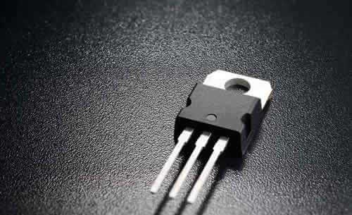
The TPS22918DBVR is available in a tiny, leaded SOT-23 package (DBV) that enables visual solder joint inspection. The gadget is designed to operate in a temperature range of –40°C to +105°C in free air.
TPS22918DBVR Pinout
The following shows TPS22918DBVR Pinout.

Pinout
| Pin Number | Pin Name | Description |
| 1 | VIN | Switch input. Place ceramic bypass capacitor(s) between this pin and GND. |
| 2 | GND | Device ground. |
| 3 | ON | Active high switch control input. Do not leave floating. |
| 4 | CT | Switch slew rate control. Can be left floating. |
| 5 | QOD | Quick Output Discharge pin. This functionality can be enabled in one of three ways. • Placing an external resistor between VOUT and QOD • Tying QOD directly to VOUT and using the internal resistor value (RPD) • Disabling QOD by leaving pin floating |
| 6 | VOUT | Switch output. |
TPS22918DBVR CAD Model


TPS22918DBVR Features
• Integrated Single Channel Load Switch
• Ambient Operating Temperature: –40°C to +105°C
• Input Voltage Range: 1 V to 5.5 V
• On-Resistance (RON)
– RON = 52 mΩ (typical) at VIN = 5 V
– RON = 53 mΩ (typical) at VIN = 3.3 V
• 2-A Maximum Continuous Switch Current
• Low Quiescent Current
– 8.3 µA (typical) at VIN = 3.3 V
• Low-Control Input-Threshold Enables Use of 1 V or Higher GPIO
• Adjustable Quick-Output Discharge (QOD)
• Configurable Rise Time With CT Pin
• Small SOT23-6 Package (DBV)
– 2.90-mm × 2.80-mm, 0.95-mm Pitch, 1.45 mm Height (with leads)
• ESD Performance Tested per JESD 22
– ±2-kV HBM and ±1-kV CDM
Specifications
- TypeParameter
- Lifecycle Status
Lifecycle Status refers to the current stage of an electronic component in its product life cycle, indicating whether it is active, obsolete, or transitioning between these states. An active status means the component is in production and available for purchase. An obsolete status indicates that the component is no longer being manufactured or supported, and manufacturers typically provide a limited time frame for support. Understanding the lifecycle status is crucial for design engineers to ensure continuity and reliability in their projects.
ACTIVE (Last Updated: 17 hours ago) - Factory Lead Time6 Weeks
- Mounting Type
The "Mounting Type" in electronic components refers to the method used to attach or connect a component to a circuit board or other substrate, such as through-hole, surface-mount, or panel mount.
Surface Mount - Package / Case
refers to the protective housing that encases an electronic component, providing mechanical support, electrical connections, and thermal management.
SOT-23-6 - Surface Mount
having leads that are designed to be soldered on the side of a circuit board that the body of the component is mounted on.
YES - Number of Pins6
- Operating Temperature
The operating temperature is the range of ambient temperature within which a power supply, or any other electrical equipment, operate in. This ranges from a minimum operating temperature, to a peak or maximum operating temperature, outside which, the power supply may fail.
-40°C~105°C TA - Packaging
Semiconductor package is a carrier / shell used to contain and cover one or more semiconductor components or integrated circuits. The material of the shell can be metal, plastic, glass or ceramic.
Tape & Reel (TR) - JESD-609 Code
The "JESD-609 Code" in electronic components refers to a standardized marking code that indicates the lead-free solder composition and finish of electronic components for compliance with environmental regulations.
e3 - Pbfree Code
The "Pbfree Code" parameter in electronic components refers to the code or marking used to indicate that the component is lead-free. Lead (Pb) is a toxic substance that has been widely used in electronic components for many years, but due to environmental concerns, there has been a shift towards lead-free alternatives. The Pbfree Code helps manufacturers and users easily identify components that do not contain lead, ensuring compliance with regulations and promoting environmentally friendly practices. It is important to pay attention to the Pbfree Code when selecting electronic components to ensure they meet the necessary requirements for lead-free applications.
yes - Part Status
Parts can have many statuses as they progress through the configuration, analysis, review, and approval stages.
Active - Moisture Sensitivity Level (MSL)
Moisture Sensitivity Level (MSL) is a standardized rating that indicates the susceptibility of electronic components, particularly semiconductors, to moisture-induced damage during storage and the soldering process, defining the allowable exposure time to ambient conditions before they require special handling or baking to prevent failures
2 (1 Year) - Number of Terminations6
- Terminal Finish
Terminal Finish refers to the surface treatment applied to the terminals or leads of electronic components to enhance their performance and longevity. It can improve solderability, corrosion resistance, and overall reliability of the connection in electronic assemblies. Common finishes include nickel, gold, and tin, each possessing distinct properties suitable for various applications. The choice of terminal finish can significantly impact the durability and effectiveness of electronic devices.
Matte Tin (Sn) - Terminal Position
In electronic components, the term "Terminal Position" refers to the physical location of the connection points on the component where external electrical connections can be made. These connection points, known as terminals, are typically used to attach wires, leads, or other components to the main body of the electronic component. The terminal position is important for ensuring proper connectivity and functionality of the component within a circuit. It is often specified in technical datasheets or component specifications to help designers and engineers understand how to properly integrate the component into their circuit designs.
DUAL - Terminal Form
Occurring at or forming the end of a series, succession, or the like; closing; concluding.
GULL WING - Number of Functions1
- Supply Voltage
Supply voltage refers to the electrical potential difference provided to an electronic component or circuit. It is crucial for the proper operation of devices, as it powers their functions and determines performance characteristics. The supply voltage must be within specified limits to ensure reliability and prevent damage to components. Different electronic devices have specific supply voltage requirements, which can vary widely depending on their design and intended application.
1V - Terminal Pitch
The center distance from one pole to the next.
0.95mm - Base Part Number
The "Base Part Number" (BPN) in electronic components serves a similar purpose to the "Base Product Number." It refers to the primary identifier for a component that captures the essential characteristics shared by a group of similar components. The BPN provides a fundamental way to reference a family or series of components without specifying all the variations and specific details.
TPS22918 - Number of Outputs1
- Output Type
The "Output Type" parameter in electronic components refers to the type of signal or data that is produced by the component as an output. This parameter specifies the nature of the output signal, such as analog or digital, and can also include details about the voltage levels, current levels, frequency, and other characteristics of the output signal. Understanding the output type of a component is crucial for ensuring compatibility with other components in a circuit or system, as well as for determining how the output signal can be utilized or processed further. In summary, the output type parameter provides essential information about the nature of the signal that is generated by the electronic component as its output.
N-Channel - Max Output Current
The maximum current that can be supplied to the load.
2A - Supply Voltage-Max (Vsup)
The parameter "Supply Voltage-Max (Vsup)" in electronic components refers to the maximum voltage that can be safely applied to the component without causing damage. It is an important specification to consider when designing or using electronic circuits to ensure the component operates within its safe operating limits. Exceeding the maximum supply voltage can lead to overheating, component failure, or even permanent damage. It is crucial to adhere to the specified maximum supply voltage to ensure the reliable and safe operation of the electronic component.
5.5V - Number of Channels1
- Interface
In electronic components, the term "Interface" refers to the point at which two different systems, devices, or components connect and interact with each other. It can involve physical connections such as ports, connectors, or cables, as well as communication protocols and standards that facilitate the exchange of data or signals between the connected entities. The interface serves as a bridge that enables seamless communication and interoperability between different parts of a system or between different systems altogether. Designing a reliable and efficient interface is crucial in ensuring proper functionality and performance of electronic components and systems.
On/Off - Analog IC - Other Type
Analog IC - Other Type is a parameter used to categorize electronic components that are integrated circuits (ICs) designed for analog signal processing but do not fall into more specific subcategories such as amplifiers, comparators, or voltage regulators. These ICs may include specialized analog functions such as analog-to-digital converters (ADCs), digital-to-analog converters (DACs), voltage references, or signal conditioning circuits. They are typically used in various applications where precise analog signal processing is required, such as in audio equipment, instrumentation, communication systems, and industrial control systems. Manufacturers provide detailed specifications for these components to help engineers select the most suitable IC for their specific design requirements.
POWER SUPPLY SUPPORT CIRCUIT - Output Configuration
Output Configuration in electronic components refers to the arrangement or setup of the output pins or terminals of a device. It defines how the output signals are structured and how they interact with external circuits or devices. The output configuration can determine the functionality and compatibility of the component in a circuit design. Common types of output configurations include single-ended, differential, open-drain, and push-pull configurations, each serving different purposes and applications in electronic systems. Understanding the output configuration of a component is crucial for proper integration and operation within a circuit.
High Side - Output Current
The rated output current is the maximum load current that a power supply can provide at a specified ambient temperature. A power supply can never provide more current that it's rated output current unless there is a fault, such as short circuit at the load.
2A - Voltage - Supply (Vcc/Vdd)
Voltage - Supply (Vcc/Vdd) is a key parameter in electronic components that specifies the voltage level required for the proper operation of the device. It represents the power supply voltage that needs to be provided to the component for it to function correctly. This parameter is crucial as supplying the component with the correct voltage ensures that it operates within its specified limits and performance characteristics. It is typically expressed in volts (V) and is an essential consideration when designing and using electronic circuits to prevent damage and ensure reliable operation.
Not Required - Adjustable Threshold
The "Adjustable Threshold" parameter in electronic components refers to the ability to manually set or modify the threshold level at which a specific function or operation is triggered. This feature allows users to customize the sensitivity or activation point of the component according to their specific requirements or preferences. By adjusting the threshold, users can fine-tune the performance of the component to suit different applications or environmental conditions. This flexibility in threshold adjustment can be particularly useful in various electronic devices and systems where precise control over triggering levels is necessary for optimal functionality.
NO - Input Type
Input type in electronic components refers to the classification of the signal or data that a component can accept for processing or conversion. It indicates whether the input is analog, digital, or a specific format such as TTL or CMOS. Understanding input type is crucial for ensuring compatibility between different electronic devices and circuits, as it determines how signals are interpreted and interacted with.
Non-Inverting - Switch Type
Based on their characteristics, there are basically three types of switches: Linear switches, tactile switches and clicky switches.
General Purpose - Ratio - Input:Output
The parameter "Ratio - Input:Output" in electronic components refers to the relationship between the input and output quantities of a device or system. It is a measure of how the input signal or energy is transformed or converted into the output signal or energy. This ratio is often expressed as a numerical value or percentage, indicating the efficiency or effectiveness of the component in converting the input to the desired output. A higher ratio typically signifies better performance or higher efficiency, while a lower ratio may indicate losses or inefficiencies in the conversion process. Understanding and optimizing the input-output ratio is crucial in designing and evaluating electronic components for various applications.
1:1 - Voltage - Load
Voltage - Load refers to the voltage across a load component in an electronic circuit when it is connected and operational. It represents the electrical potential difference that drives current through the load, which can be a resistor, motor, or other devices that consume electrical power. The voltage - load relationship is crucial for determining how much power the load will utilize and how it will affect the overall circuit performance. Properly managing voltage - load is essential for ensuring devices operate efficiently and safely within their specified limits.
1V~5.5V - Rds On (Typ)
The parameter "Rds On (Typ)" in electronic components refers to the typical on-state resistance of a MOSFET (Metal-Oxide-Semiconductor Field-Effect Transistor) when it is fully conducting. This parameter indicates the resistance encountered by the current flowing through the MOSFET when it is in the on-state, which affects the power dissipation and efficiency of the component. A lower Rds On value indicates better conduction and lower power loss in the MOSFET. Designers often consider this parameter when selecting components for applications where minimizing power loss and maximizing efficiency are critical factors.
53m Ω - Max Junction Temperature (Tj)
Max Junction Temperature (Tj) refers to the maximum allowable temperature at the junction of a semiconductor device, such as a transistor or integrated circuit. It is a critical parameter that influences the performance, reliability, and lifespan of the component. Exceeding this temperature can lead to thermal runaway, breakdown, or permanent damage to the device. Proper thermal management is essential to ensure the junction temperature remains within safe operating limits during device operation.
125°C - Ambient Temperature Range High
This varies from person to person, but it is somewhere between 68 and 77 degrees F on average. The temperature setting that is comfortable for an individual may fluctuate with humidity and outside temperature as well. The temperature of an air conditioned room can also be considered ambient temperature.
105°C - Features
In the context of electronic components, the term "Features" typically refers to the specific characteristics or functionalities that a particular component offers. These features can vary depending on the type of component and its intended use. For example, a microcontroller may have features such as built-in memory, analog-to-digital converters, and communication interfaces like UART or SPI.When evaluating electronic components, understanding their features is crucial in determining whether they meet the requirements of a particular project or application. Engineers and designers often look at features such as operating voltage, speed, power consumption, and communication protocols to ensure compatibility and optimal performance.In summary, the "Features" parameter in electronic components describes the unique attributes and capabilities that differentiate one component from another, helping users make informed decisions when selecting components for their electronic designs.
Load Discharge, Slew Rate Controlled - Height1.45mm
- Length2.9mm
- Width1.6mm
- Thickness
Thickness in electronic components refers to the measurement of how thick a particular material or layer is within the component structure. It can pertain to various aspects, such as the thickness of a substrate, a dielectric layer, or conductive traces. This parameter is crucial as it impacts the electrical, mechanical, and thermal properties of the component, influencing its performance and reliability in electronic circuits.
1.2mm - RoHS Status
RoHS means “Restriction of Certain Hazardous Substances” in the “Hazardous Substances Directive” in electrical and electronic equipment.
ROHS3 Compliant - Lead Free
Lead Free is a term used to describe electronic components that do not contain lead as part of their composition. Lead is a toxic material that can have harmful effects on human health and the environment, so the electronics industry has been moving towards lead-free components to reduce these risks. Lead-free components are typically made using alternative materials such as silver, copper, and tin. Manufacturers must comply with regulations such as the Restriction of Hazardous Substances (RoHS) directive to ensure that their products are lead-free and environmentally friendly.
Lead Free
Parts with Similar Specs
- ImagePart NumberManufacturerPackage / CaseNumber of PinsMax Output CurrentOutput CurrentNumber of OutputsRoHS StatusOutput ConfigurationSwitch TypeView Compare
![TPS22918DBVR]()
TPS22918DBVR
SOT-23-6
6
2 A
2 A
1
ROHS3 Compliant
High Side
General Purpose
![FDC6329L]()
SOT-23-6 Thin, TSOT-23-6
6
2.5 A
2.5 A
1
ROHS3 Compliant
High Side
General Purpose
![TPS22929DDBVR]()
SOT-23-6 Thin, TSOT-23-6
6
1.8 A
1 A
1
ROHS3 Compliant
High Side
General Purpose
![FDC6326L]()
SOT-23-6
6
1.8 A
1.8 A
1
ROHS3 Compliant
High Side
General Purpose
![MIC2019YM6-TR]()
SOT-23-6
6
2 A
-
1
ROHS3 Compliant
High Side
General Purpose


TPS22918DBVR Functional Block Diagram

TPS22918DBVR Typical Application
This typical application demonstrates how the TPS22918DBVR can be used to power downstream modules.

Typical Application
TPS22918DBVR Simplified Schematic

TPS22918DBVR Layout
To accommodate the large current, VIN and VOUT traces should be as short and wide as possible.
With low ESR ceramic bypass capacitors, the VIN pin should be routed to the ground. 1-µF ceramic with X5R or X7R dielectric is a standard recommended bypass capacitance. This capacitor should be as close as feasible to the device pins.

Recommended Board Layout
TPS22918DBVR Alternatives
| Part Number | Description | Manufacturer |
| TPS22918DBVTPOWER CIRCUITS | 5.5-V, 2-A, 52-mΩ load switch with adj. rise time and adj. output discharge 6-SOT-23 -40 to 105 | Texas Instruments |
TPS22918DBVR Applications
• Industrial Systems
• Set Top Box
• Blood Glucose Meters
• Electronic Point of Sale
TPS22918DBVR Package

TPS22918DBVR Manufacturer
Texas Instruments (TI), a multinational semiconductor business with operations in 35 countries, is first and foremost a reflection of its employees. We are problem-solvers cooperating to transform the world via technology, from the TIer who introduced the first functional integrated circuit in 1958 to the more than 30,000 TIers throughout the world today who develop, build, and distribute analog and embedded processor chips.
Trend Analysis
Datasheet PDF
- PCN Assembly/Origin :
- Datasheets :
What is a Load Switch?
A load switch is an electronic component that has no moving parts, which works somewhat like a relay.
What are the characteristics of the TPS22918DBVR?
Adjustable rise and short output discharge times.
What is included in the TPS22918DBVR?
An N-channel MOSFET.
How is the TPS22918DBVR operated?
Via an on/off input that can interface with low-voltage control signals directly.
What causes inrush current to be induced by the TPS22918DBVR?
Large bulk load capacitances.
What does the TPS22918DBVR have?
A programmable rapid output discharge (QOD) pin.
What package is the TPS22918DBVR available in?
SOT-23.
What is the temperature range of the TPS22918DBVR?
–40°C to +105°C.
 A Comprehensive Guide to LTC6953IUKG#TRPBF Clock Generator by Linear Technology/Analog Devices
06 March 2024243
 STS4DNF60L:datasheet, pinout and specifications
11 March 2022406
 PIC12F629 Microcontroller: Features, Pinout, and Datasheet
07 December 20216825
 Exploring the Microchip PIC16C6X 8-Bit CMOS Microcontrollers
29 February 2024235
 2N5551 Transistor: Pinout, Datasheet, and Applications
09 July 202113263
 LTC6803IG-2#PBF Battery Management IC: Product Overview and Applications
06 March 2024108
![FDG6335N N-Channel MOSFET: Diagram, Pinout, and Datasheet [Video&FAQ]](https://res.utmel.com/Images/Article/ed8c0389-8d09-46cf-91fb-43c5dd0cf724.png) FDG6335N N-Channel MOSFET: Diagram, Pinout, and Datasheet [Video&FAQ]
FDG6335N N-Channel MOSFET: Diagram, Pinout, and Datasheet [Video&FAQ]28 April 20221922
 LM1875T/NOPB Audio Amplifier: Feature,Specification,Datasheet
17 May 20214075
 What is the DC Bias Characteristic of a Capacitor?
25 July 202211130
 Will AI Eventually Compete With Humans for Energy Resources?
14 February 20234221
 Design and Implementation of High Frequency Inverter for Printer Based on IR2110
13 April 20229188
 Nexperia Enters the Analog Chip Market
23 March 2022870
 What is Uninterruptible Power Supply (UPS)?
08 April 20214833
 The Difference between Switching Power Supply and Ordinary Power Supply
12 July 20221655
 Gartner: Hysis Revenue Plunges 81%, Samsung Holds on to Semiconductor Leadership
15 April 2022851
 What are Varactor Diodes?
24 November 20259334
Texas Instruments
In Stock: 997
United States
China
Canada
Japan
Russia
Germany
United Kingdom
Singapore
Italy
Hong Kong(China)
Taiwan(China)
France
Korea
Mexico
Netherlands
Malaysia
Austria
Spain
Switzerland
Poland
Thailand
Vietnam
India
United Arab Emirates
Afghanistan
Åland Islands
Albania
Algeria
American Samoa
Andorra
Angola
Anguilla
Antigua & Barbuda
Argentina
Armenia
Aruba
Australia
Azerbaijan
Bahamas
Bahrain
Bangladesh
Barbados
Belarus
Belgium
Belize
Benin
Bermuda
Bhutan
Bolivia
Bonaire, Sint Eustatius and Saba
Bosnia & Herzegovina
Botswana
Brazil
British Indian Ocean Territory
British Virgin Islands
Brunei
Bulgaria
Burkina Faso
Burundi
Cabo Verde
Cambodia
Cameroon
Cayman Islands
Central African Republic
Chad
Chile
Christmas Island
Cocos (Keeling) Islands
Colombia
Comoros
Congo
Congo (DRC)
Cook Islands
Costa Rica
Côte d’Ivoire
Croatia
Cuba
Curaçao
Cyprus
Czechia
Denmark
Djibouti
Dominica
Dominican Republic
Ecuador
Egypt
El Salvador
Equatorial Guinea
Eritrea
Estonia
Eswatini
Ethiopia
Falkland Islands
Faroe Islands
Fiji
Finland
French Guiana
French Polynesia
Gabon
Gambia
Georgia
Ghana
Gibraltar
Greece
Greenland
Grenada
Guadeloupe
Guam
Guatemala
Guernsey
Guinea
Guinea-Bissau
Guyana
Haiti
Honduras
Hungary
Iceland
Indonesia
Iran
Iraq
Ireland
Isle of Man
Israel
Jamaica
Jersey
Jordan
Kazakhstan
Kenya
Kiribati
Kosovo
Kuwait
Kyrgyzstan
Laos
Latvia
Lebanon
Lesotho
Liberia
Libya
Liechtenstein
Lithuania
Luxembourg
Macao(China)
Madagascar
Malawi
Maldives
Mali
Malta
Marshall Islands
Martinique
Mauritania
Mauritius
Mayotte
Micronesia
Moldova
Monaco
Mongolia
Montenegro
Montserrat
Morocco
Mozambique
Myanmar
Namibia
Nauru
Nepal
New Caledonia
New Zealand
Nicaragua
Niger
Nigeria
Niue
Norfolk Island
North Korea
North Macedonia
Northern Mariana Islands
Norway
Oman
Pakistan
Palau
Palestinian Authority
Panama
Papua New Guinea
Paraguay
Peru
Philippines
Pitcairn Islands
Portugal
Puerto Rico
Qatar
Réunion
Romania
Rwanda
Samoa
San Marino
São Tomé & Príncipe
Saudi Arabia
Senegal
Serbia
Seychelles
Sierra Leone
Sint Maarten
Slovakia
Slovenia
Solomon Islands
Somalia
South Africa
South Sudan
Sri Lanka
St Helena, Ascension, Tristan da Cunha
St. Barthélemy
St. Kitts & Nevis
St. Lucia
St. Martin
St. Pierre & Miquelon
St. Vincent & Grenadines
Sudan
Suriname
Svalbard & Jan Mayen
Sweden
Syria
Tajikistan
Tanzania
Timor-Leste
Togo
Tokelau
Tonga
Trinidad & Tobago
Tunisia
Turkey
Turkmenistan
Turks & Caicos Islands
Tuvalu
U.S. Outlying Islands
U.S. Virgin Islands
Uganda
Ukraine
Uruguay
Uzbekistan
Vanuatu
Vatican City
Venezuela
Wallis & Futuna
Yemen
Zambia
Zimbabwe
![TPS22913CYZVR]() TPS22913CYZVR
TPS22913CYZVRTexas Instruments
![TPS2052BDR]() TPS2052BDR
TPS2052BDRTexas Instruments
![TPS2051BDGNR]() TPS2051BDGNR
TPS2051BDGNRTexas Instruments
![TPS2044BD]() TPS2044BD
TPS2044BDTexas Instruments
![TPS2042BDR]() TPS2042BDR
TPS2042BDRTexas Instruments
![ULQ2003ADR]() ULQ2003ADR
ULQ2003ADRTexas Instruments
![TPS22945DCKR]() TPS22945DCKR
TPS22945DCKRTexas Instruments
![TPS2042BDGN]() TPS2042BDGN
TPS2042BDGNTexas Instruments
![TPS2557DRBT]() TPS2557DRBT
TPS2557DRBTTexas Instruments
![TPS2044BDR]() TPS2044BDR
TPS2044BDRTexas Instruments


